Introduction
We have recently received the IQ8P microinverter from Enphase. It features a durable engineered plastic enclosure and comes with a 15-year warranty. It supports 60- to 78-cell PV modules, delivers an output power of up to 480 VA, and is suitable for both grid-tied and off-grid applications. The maximum DC input voltage is 65 V, with peak power tracking supported between 36–55 V. The maximum continuous input current is 14 A, and the maximum short-circuit input current is 25 A. The DC input side is equipped with an adapter cable for connecting to standard MC4 connectors. Next, let’s take it apart to see its internal components and structure.
Product Appearance

Under the black plastic enclosure, there are screw holes and input/output sockets.
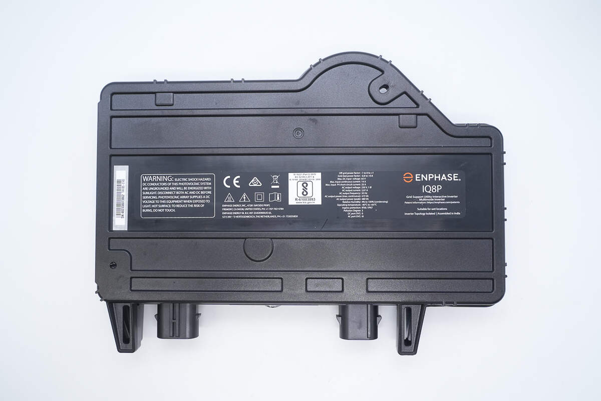
An information label is affixed to the front.
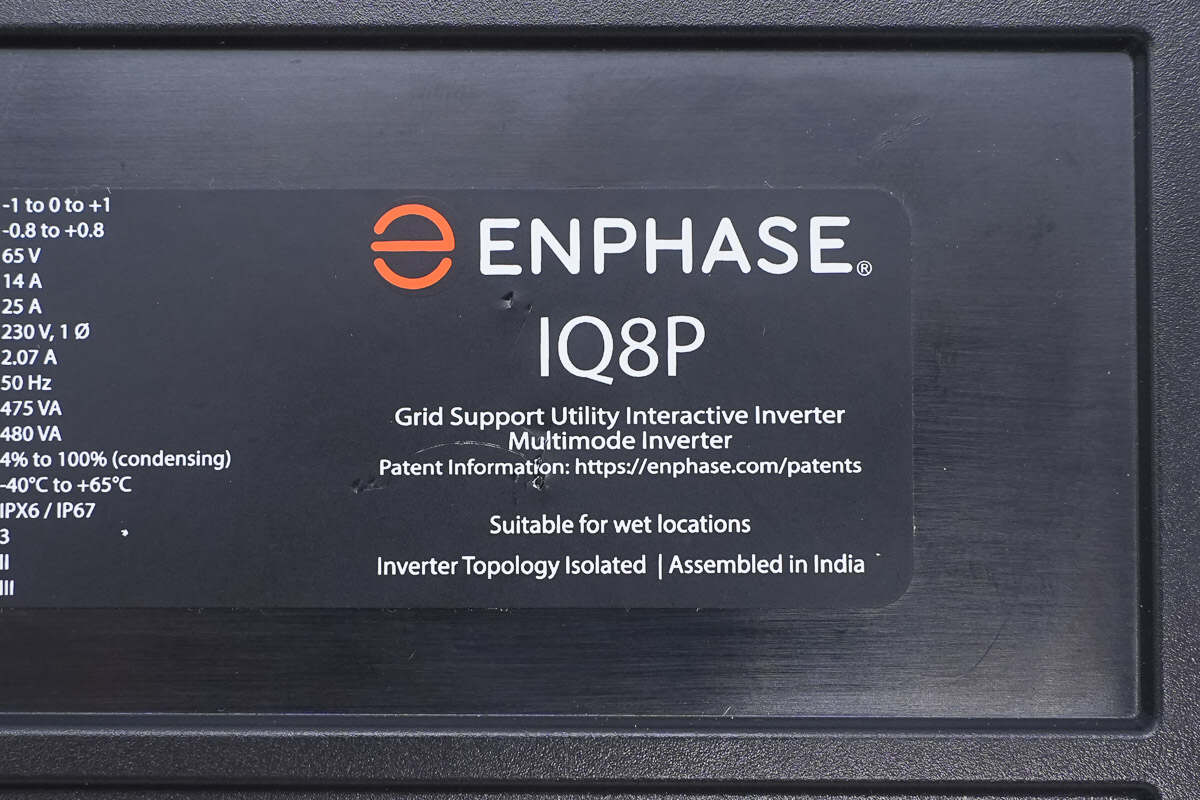
The label indicates the brand and model IQ8P, and states that it is suitable for use in wet locations.
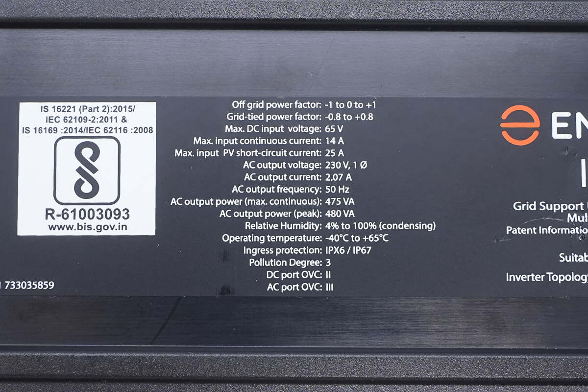
Off-grid power factor: -1 to 0 to +1
Grid-tied power factor: -0.8 to +0.8
Maximum DC input voltage: 65 V
Maximum continuous DC input current: 14 A
Maximum DC short-circuit current: 25 A
AC output voltage: 230 V
AC output current: 2.07 A
AC output frequency: 50 Hz
AC output power (maximum continuous): 475 VA
AC output power (peak): 480 VA
Relative humidity: 4%–100%
Operating temperature: -40℃ to 65℃
Ingress protection rating: IP67
Pollution degree: 3
DC port overvoltage category: II
AC port overvoltage category: III
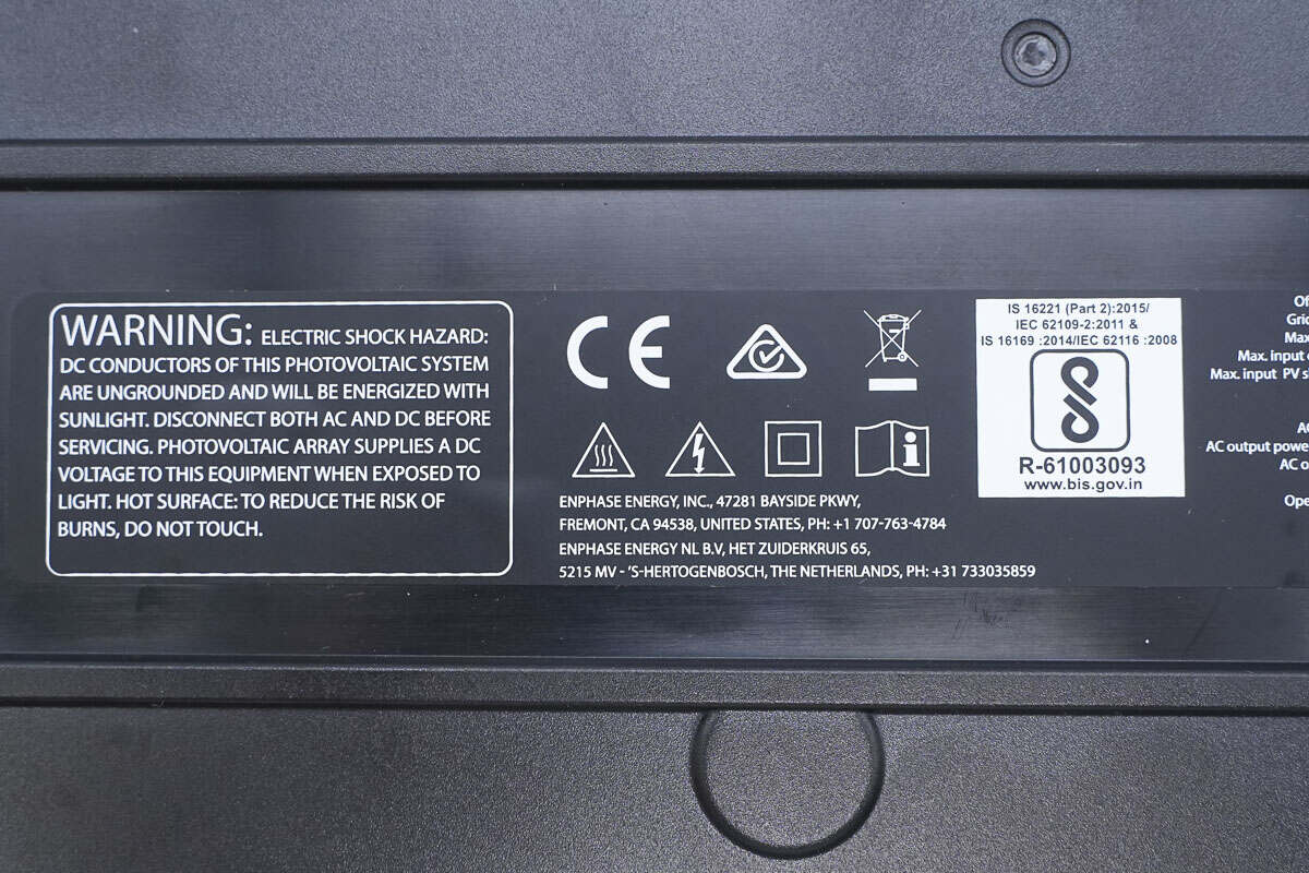
Safety warnings are indicated.
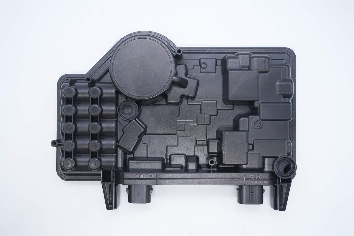
The other side reveals the shape of the internal components, with "DC" and "AC" labeled above the respective connectors.
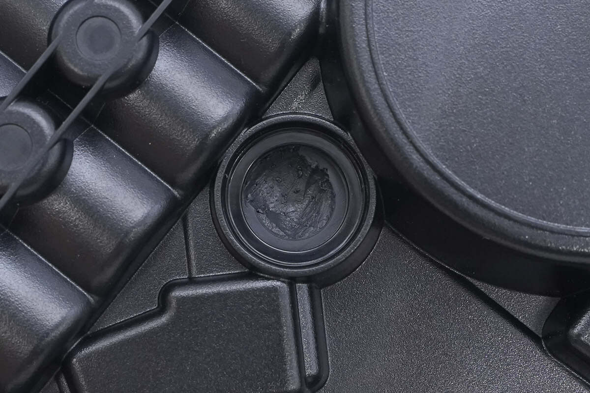
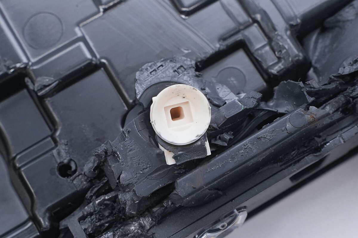
Close-up of the potting compound injection port.
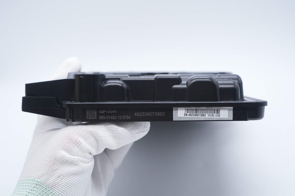
The model number is printed on the side, and a serial number sticker is affixed.
Close-up of the enclosure seam.
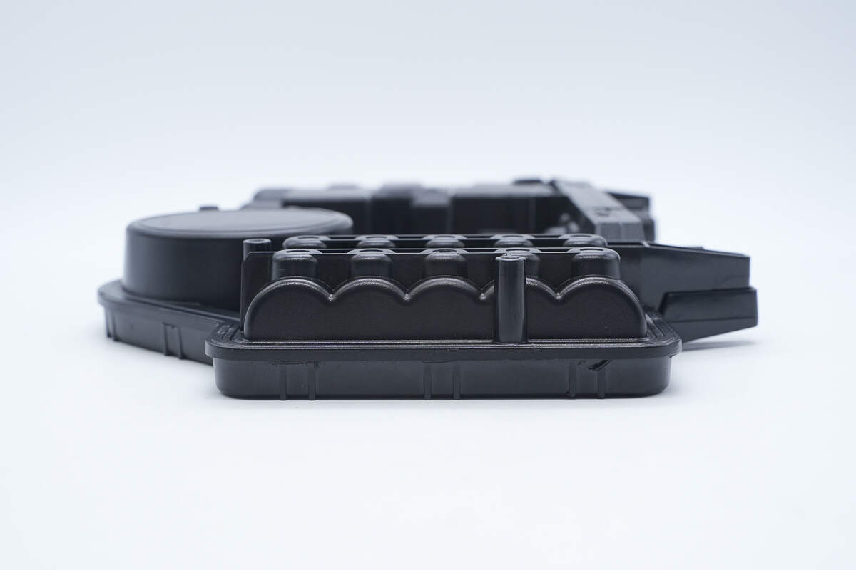
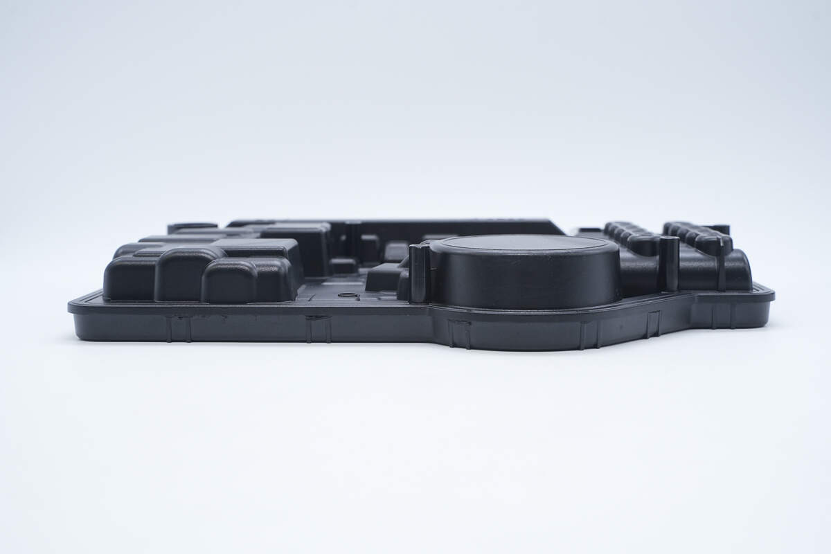
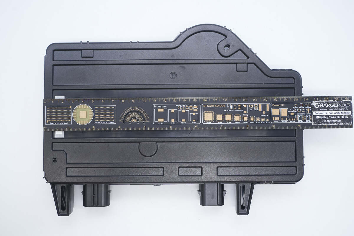
The other side of the enclosure conforms to the shape of the internal components.
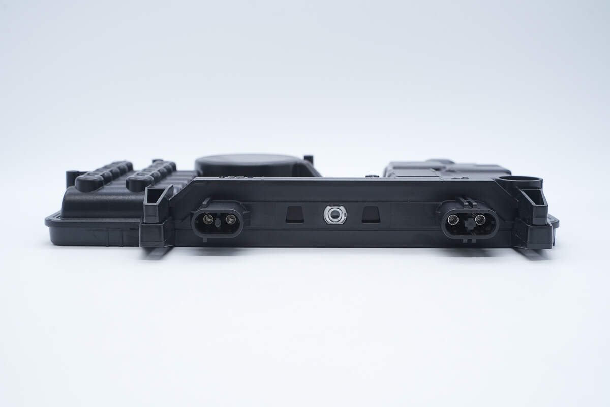
Close-up of the DC input connector, indicator light, and AC output connector.
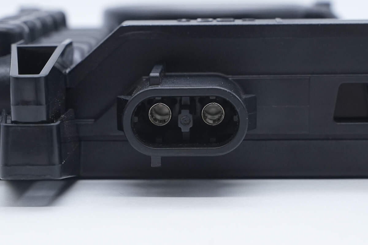
The DC input connector has a reverse polarity protection design.
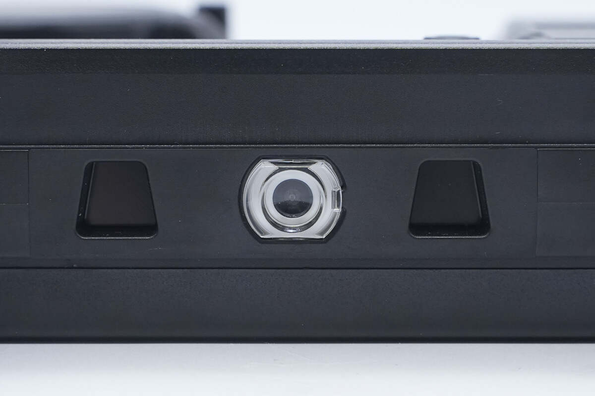
Close-up of the indicator light.
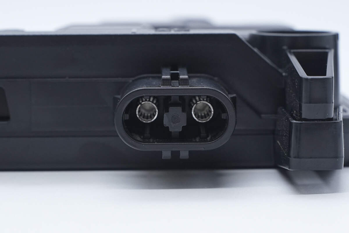
Close-up of the AC output connector.
The length of the microinverter is about 26 cm (10.24 inches).
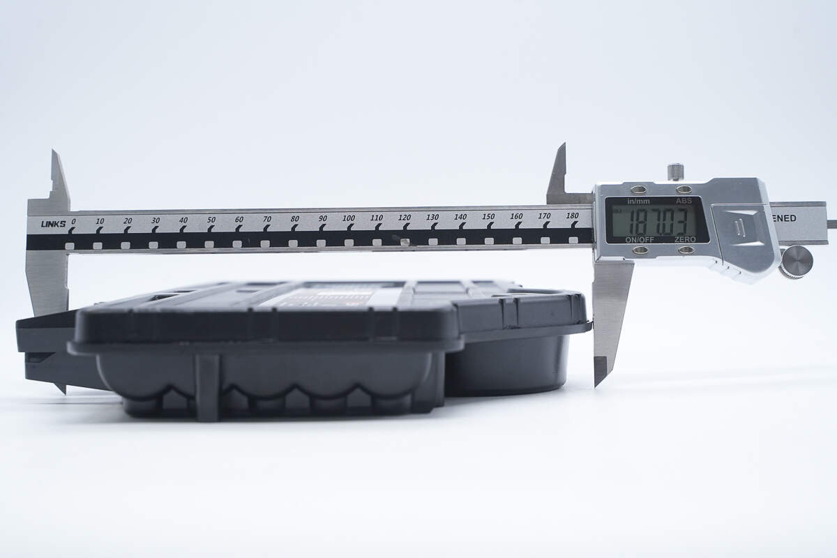
The width is about 187 mm (7.36 inches).

The thickness is about 34 mm (1.34 inches).
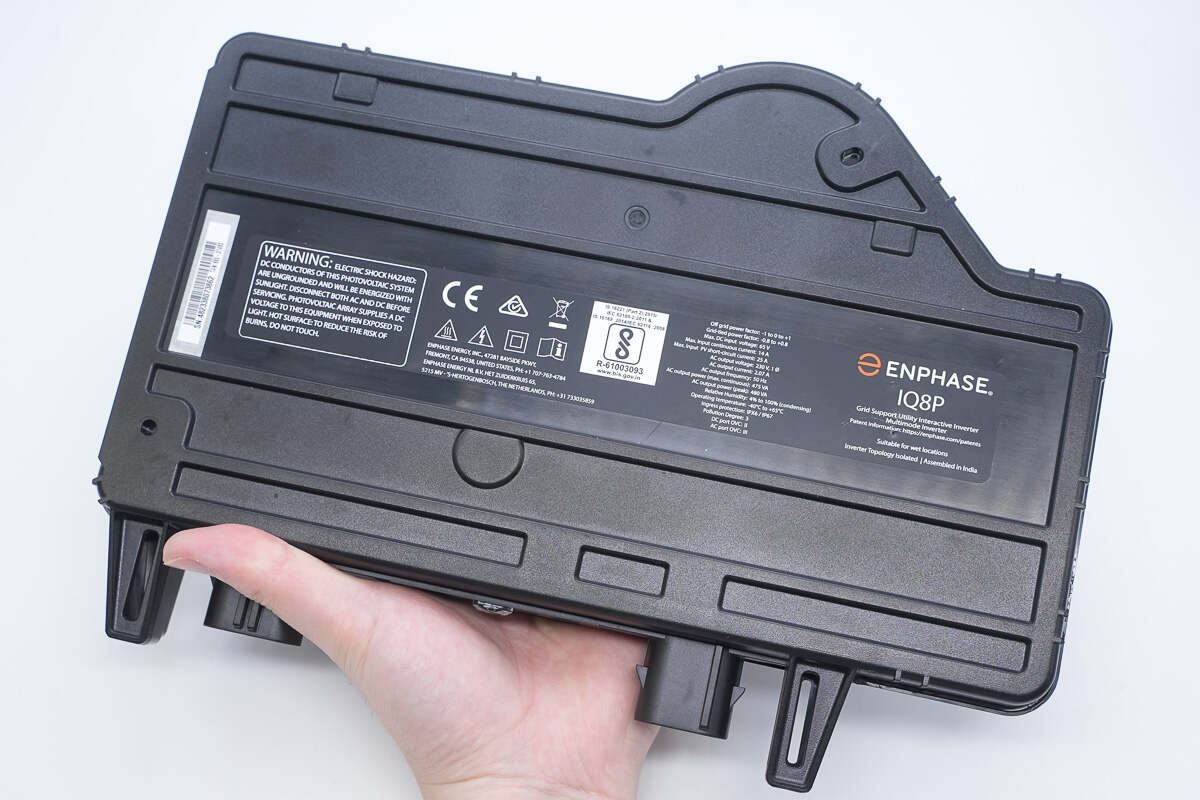
That's how big it is in the hand.
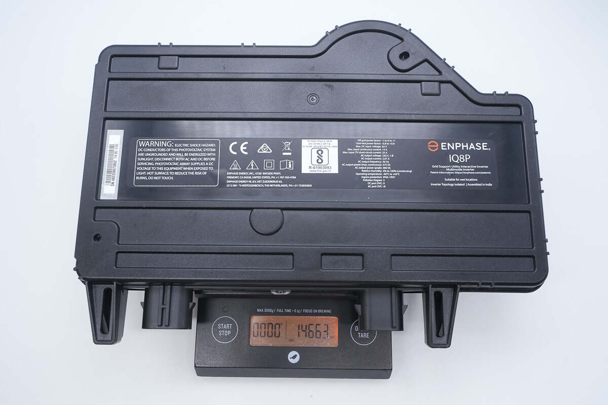
The weight is about 1466 g (3.232 lbs).
Teardown
Next, let's take it apart to see its internal components and structure.
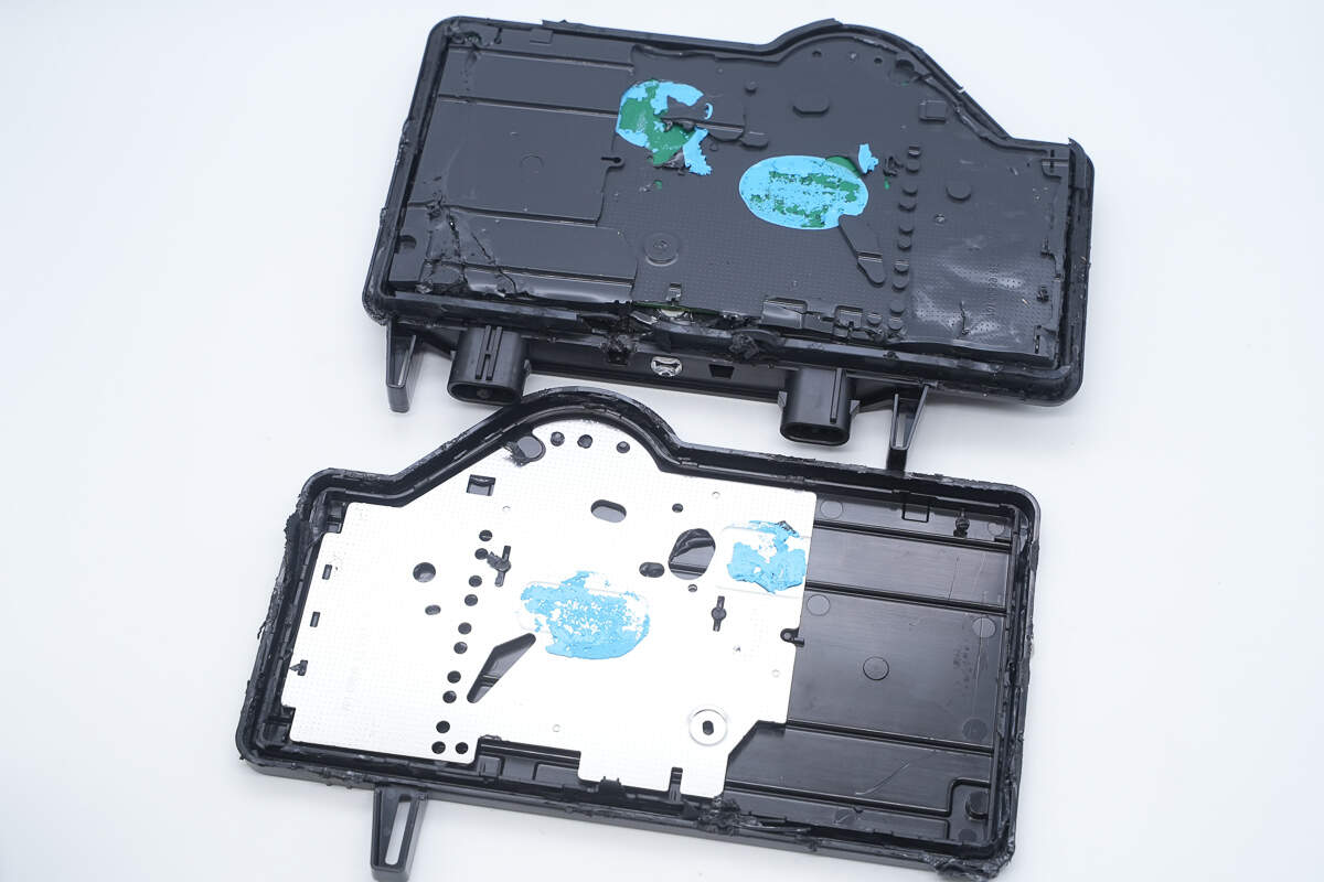
The enclosure is opened along the seam, with the interior filled with black potting compound.

Inside the cover, a heat-dissipating aluminum plate cools the PCBA module through blue thermal gel.

The black potting compound has imprinted the shapes of the heat sink plate and the inside of the cover.
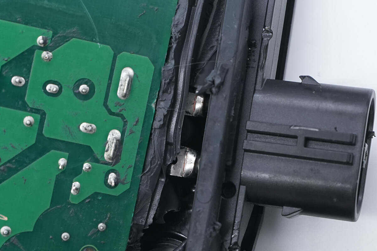
The DC input and AC output connectors are connected by soldering.
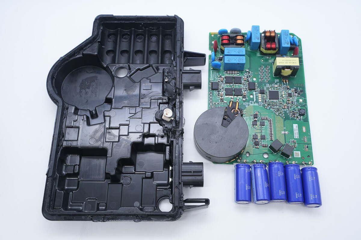
Take out the PCBA module.
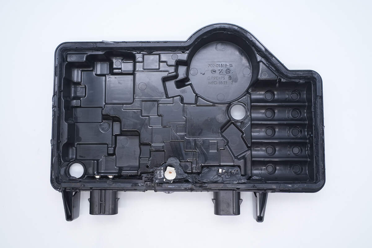
The interior of the enclosure is shaped to fit the components and is made of PPE+PS material.
Close-up of the light guide structure for the indicator LED.
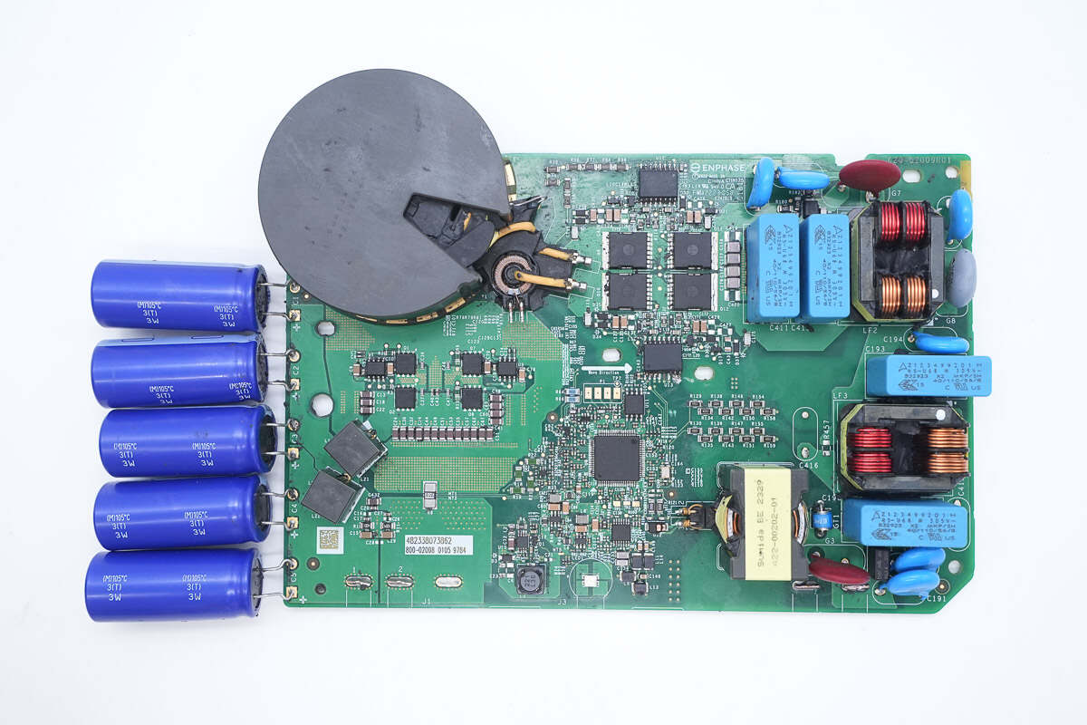
On the left side of the PCBA module is the DC input end, which has filter capacitors, filter inductors, buck MOSFETs, a driver, and a transformer. In the middle, there is a master control chip, isolation drivers, and MOSFETs. On the right side, there is an output filter circuit and a power line communication circuit.
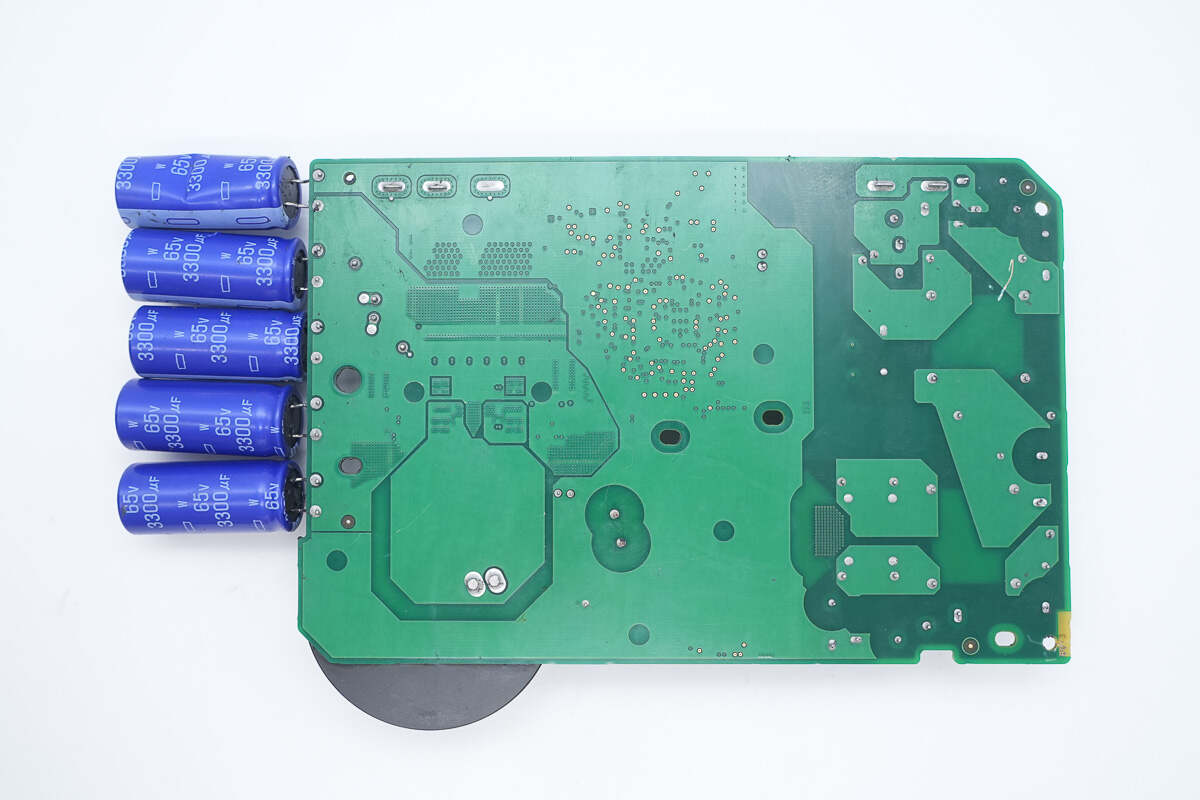
There are no components on the back.
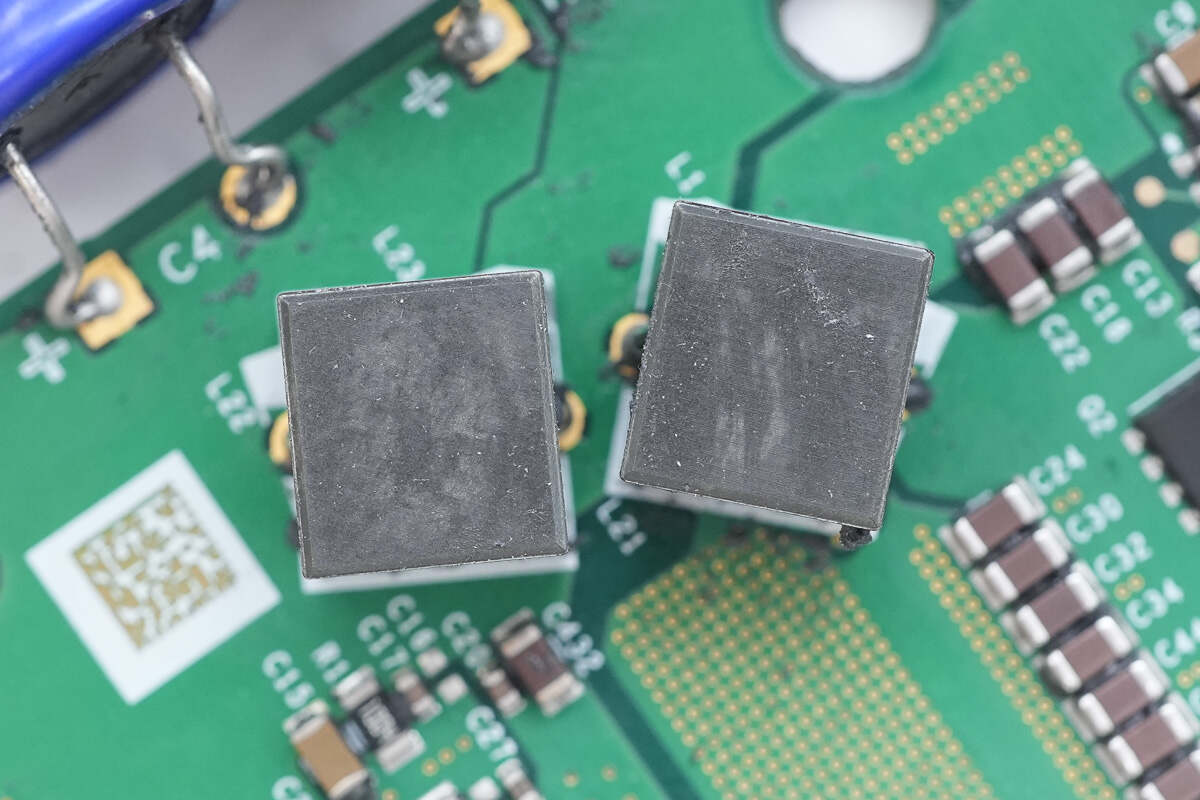
Close-up of the two filter inductors at the input end.
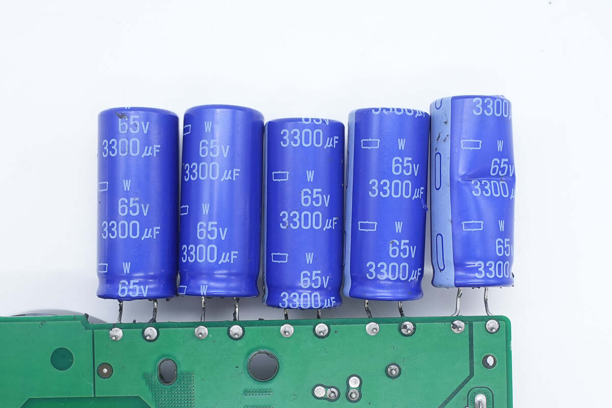
The electrolytic capacitors are from NCC, rated at 65V 3300μF, with five used for input filtering.
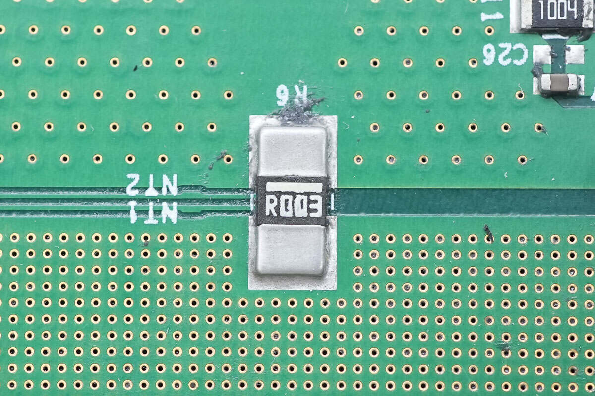
A 3mΩ shunt resistor is used to measure the inverter’s input current.
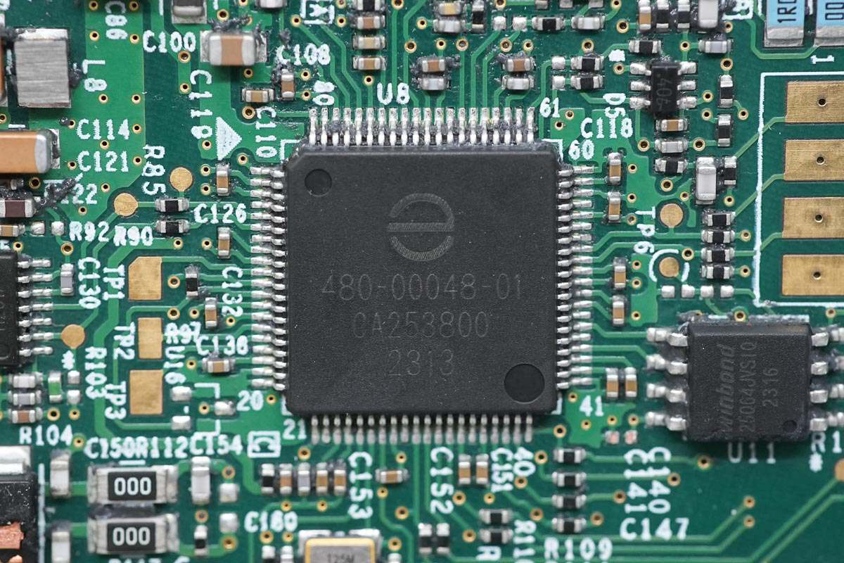
The master control chip, sourced from ENPHASE and marked with 480-00048-01, generates control signals for both DC boost and output modulation. The DC boost is driven by a half-bridge driver, while the AC modulation is driven through isolation drivers. The chip uses an LQFP80 package.
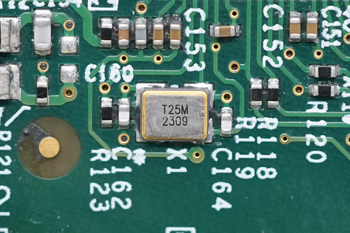
Close-up of the external clock crystal oscillator for the master control chip.

The external memory for the master control chip is from Winbond, model W25Q64JVSSIQ, with a capacity of 8MB, packaged in SOP8.

Close-up of the indicator LED.
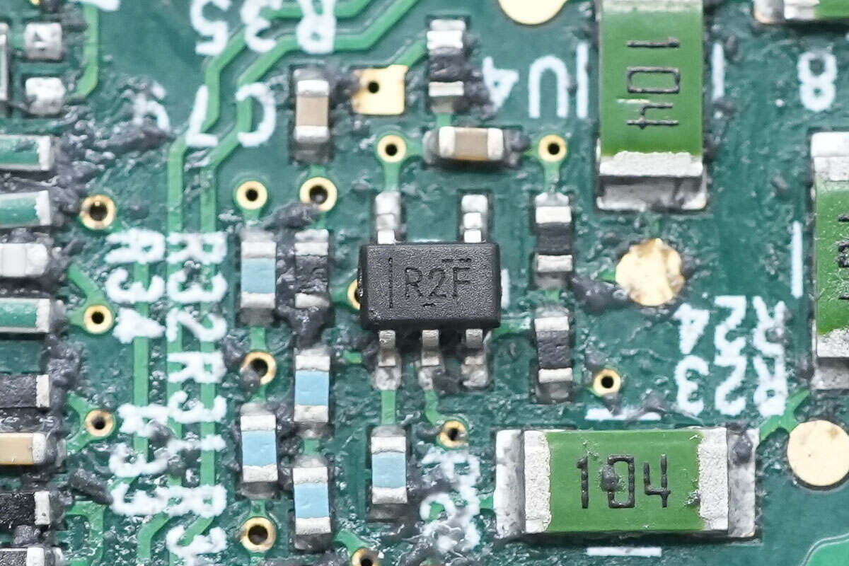
The voltage comparator is from TI, marked with R2F, model LMV331. It is a general-purpose low-voltage comparator packaged in SC70.

Close-up of the series voltage divider resistors used for voltage sampling.
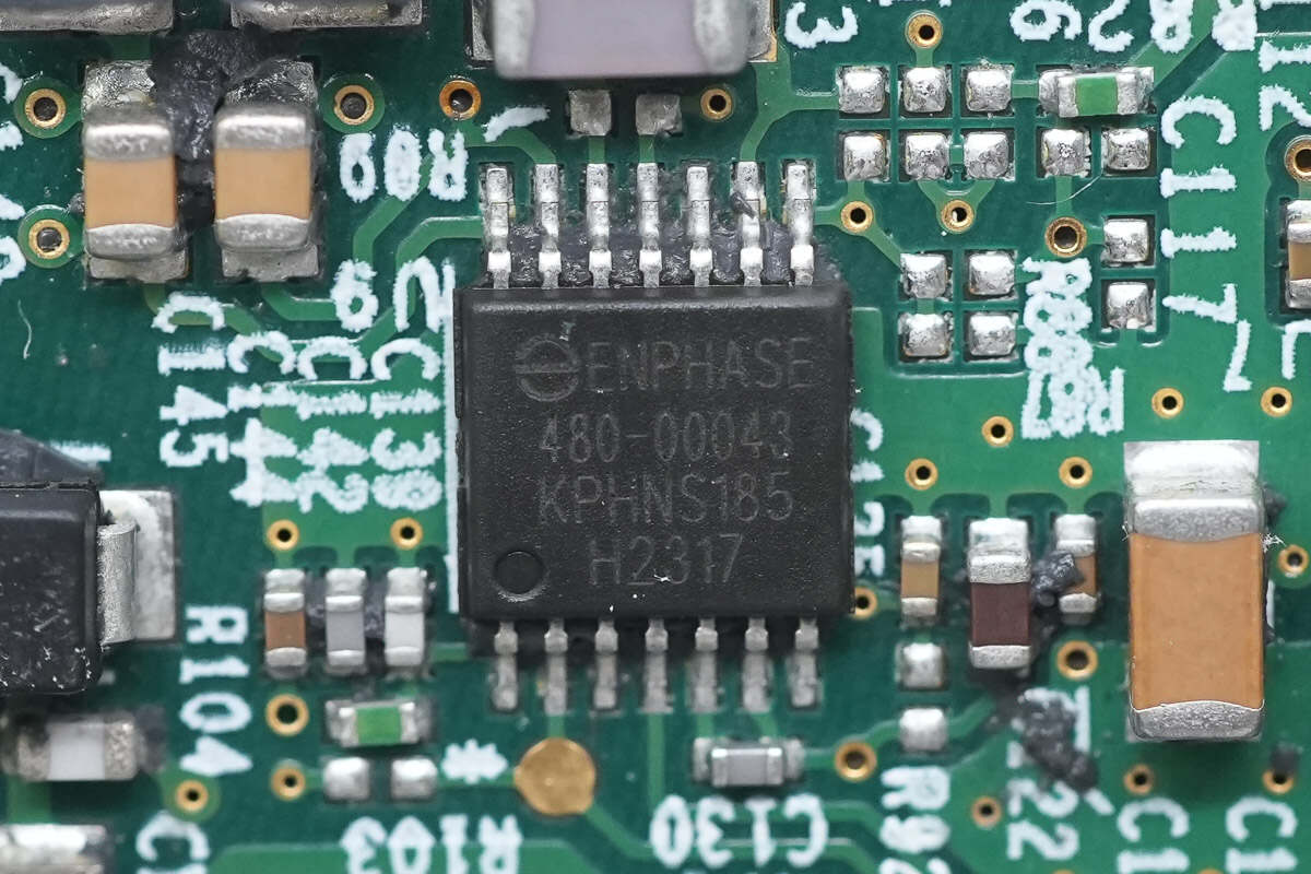
Another ENPHASE custom chip, marked with 480-00043 and housed in a TSSOP14 package, is used for power line communication functionality.
Close-up of the external inductors and capacitors for the power line communication chip.
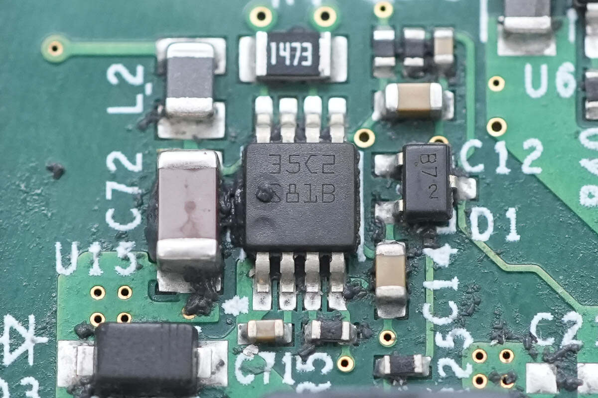
The buck converter chip is from TI, marked with S81B, model LM5007. It features an integrated MOSFET, supports 9–75 V input voltage, 0.5 A output current, ultra-fast transient response, and comprehensive protection functions. It comes in a VSSOP8 package.
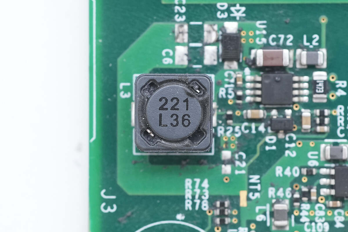
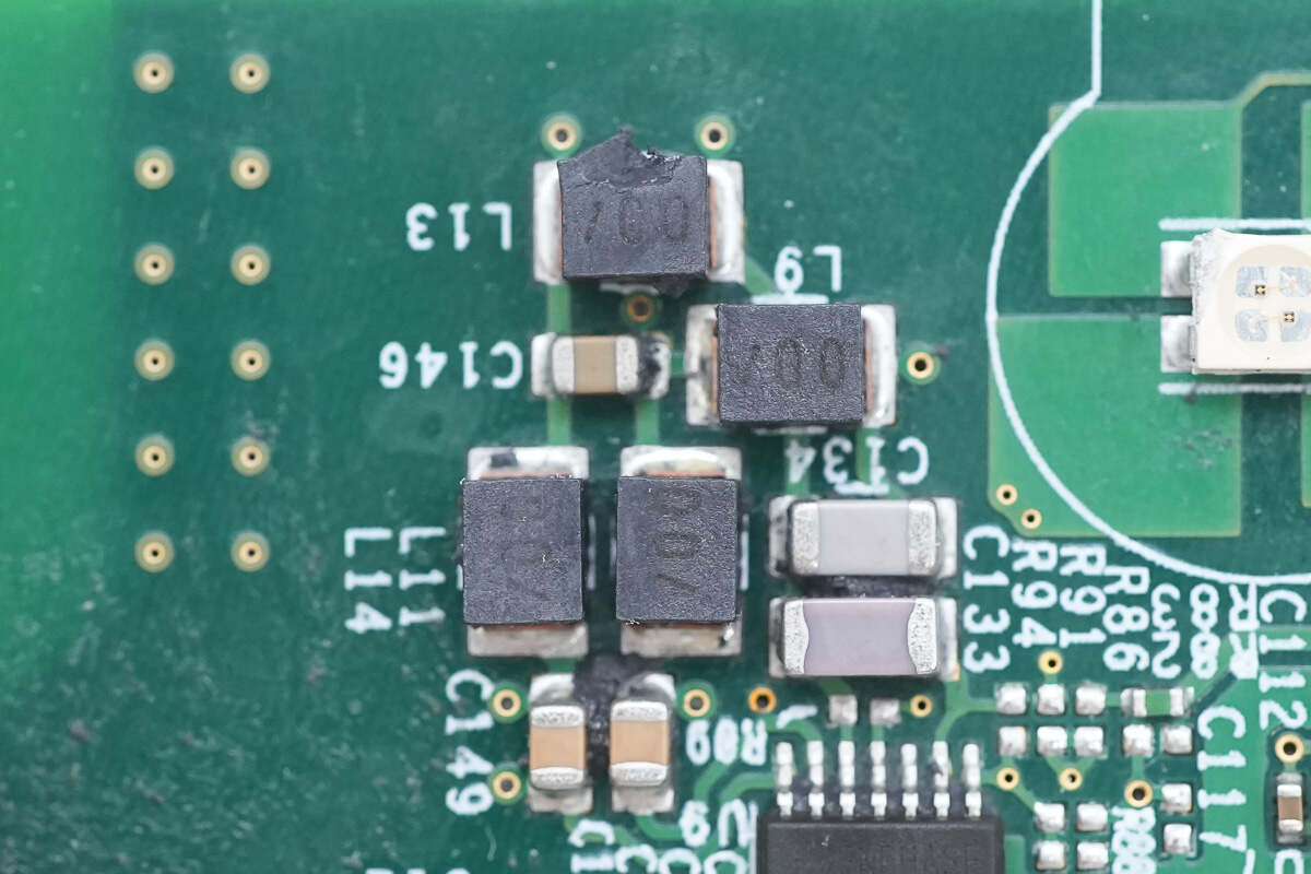
Close-up of the buck converter inductor. 220μH.
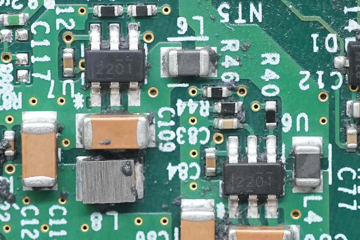
The synchronous buck chip is from TI, model TPS562201. It supports a 17 V input voltage and 2 A output current, and is packaged in SOT23.
Close-up of the DC boost circuit.
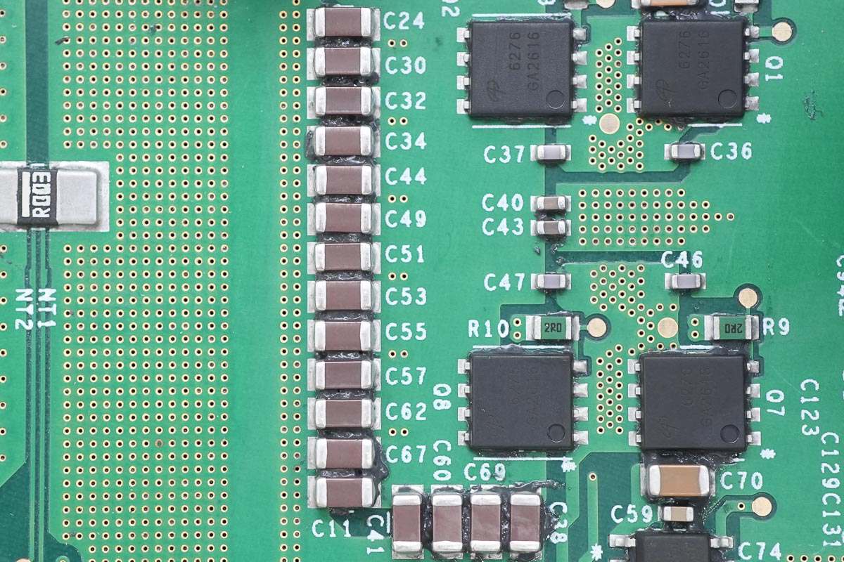
The input end uses 20 parallel-connected MLCC capacitors in 1210 packages for filtering.
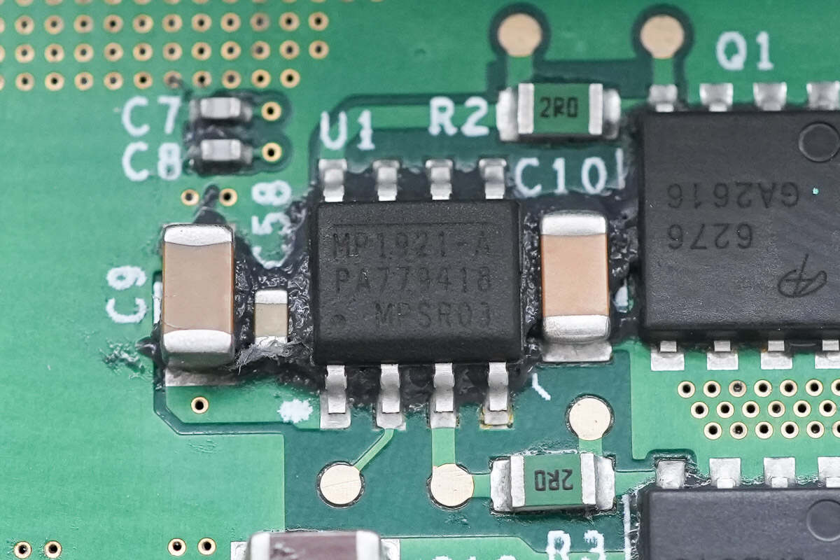
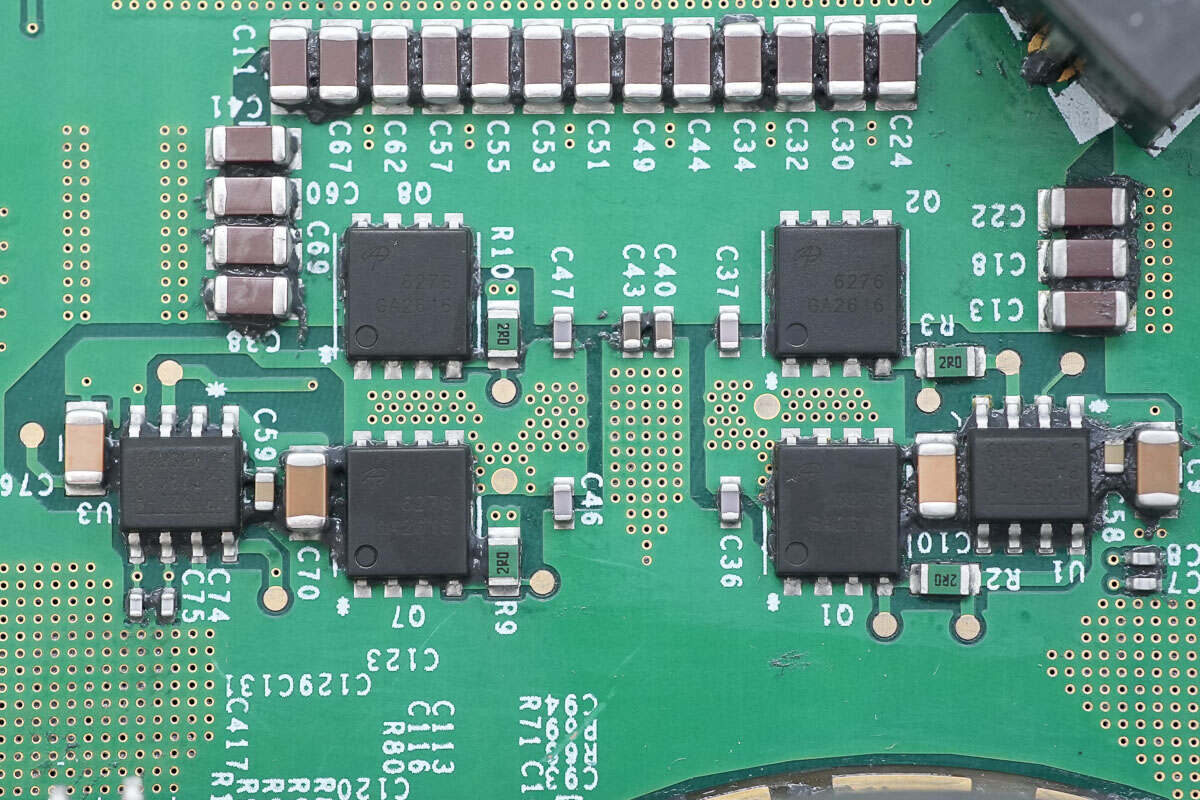
The half-bridge driver is from MPS, model MP1921A. It is a 100V half-bridge driver with a built-in bootstrap diode and comes in an SOIC-8 package.
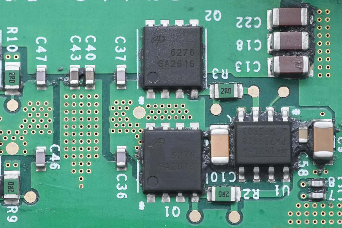
The buck MOSFETs are from AOS, model AON6276. They are NMOS devices rated for 80V, with a low on-resistance of 2.6mΩ, featuring low gate charge and low output capacitance. They come in a DFN 5×6 package.
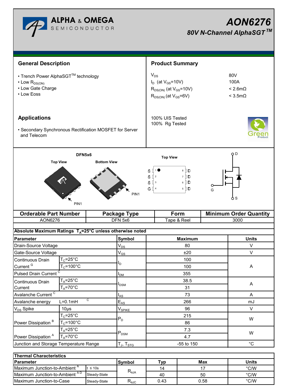
Here is the information about AOS AON6276.
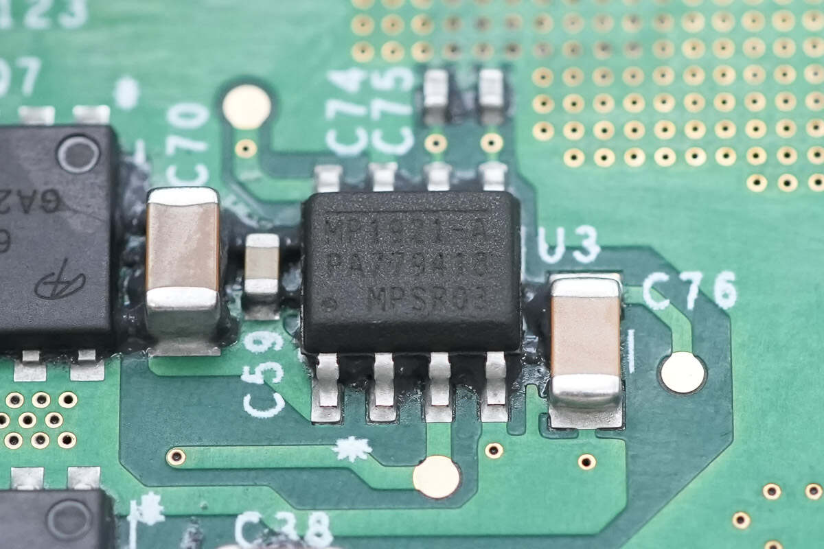
The other half-bridge driver also uses the MPS MP1921A.

These two buck MOSFETs also use the AOS AON6276.
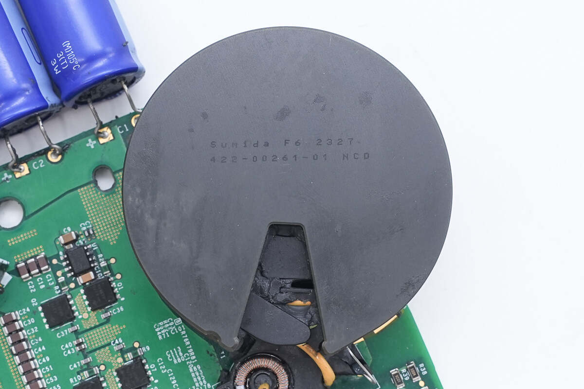
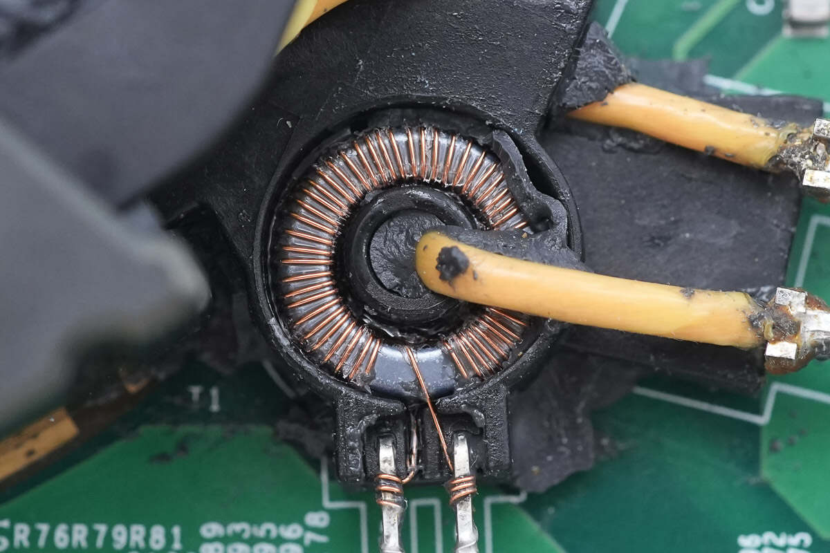
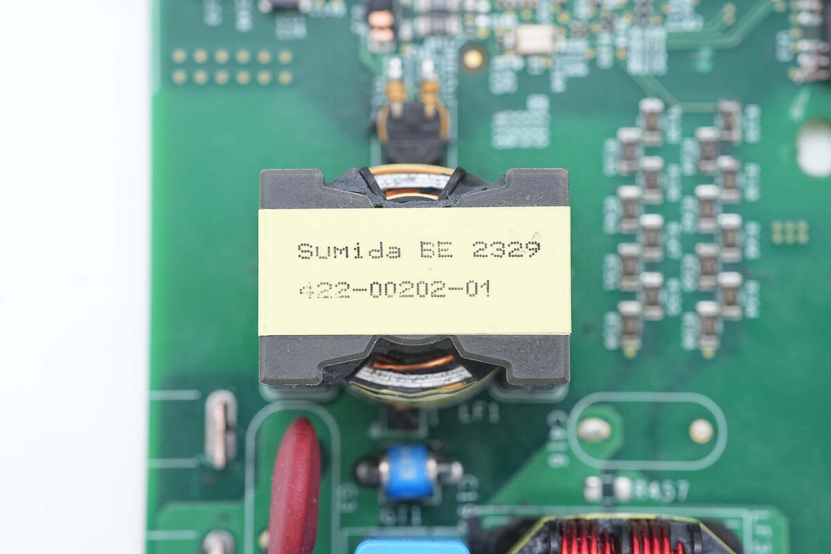
The transformer is from SUMIDA.
The output wire is equipped with a current transformer.
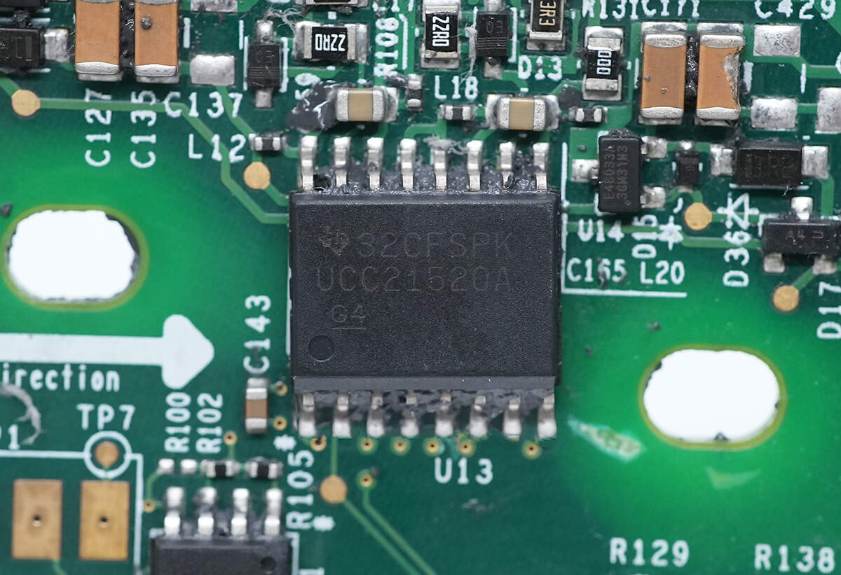
The isolation driver is from TI, model UCC21520. It is a dual-channel driver supporting dual low-side, high-side, and half-bridge applications. It provides 4A sourcing and 6A sinking current output, features capacitive isolation with 5700 Vrms isolation rating, and comes in an SOIC-16 package.

The external voltage regulator chip for the isolation driver is from ENPHASE, marked with E48033A, and comes in an SOT23 package.
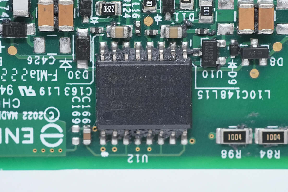
The other isolation driver also uses the TI UCC21520.
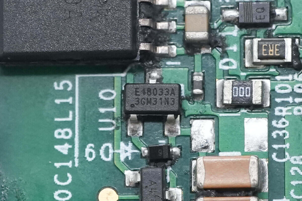
The voltage regulator chip is marked with E48033A.

The output modulation MOSFETs are from Infineon, model IPT60R050G7. They belong to the CoolMOS G7 series, are NMOS devices rated at 650 V, with an on-resistance of 50 mΩ, and come in an HSOF-8 package.

Close-up of the NPO resonant capacitors used in conjunction.
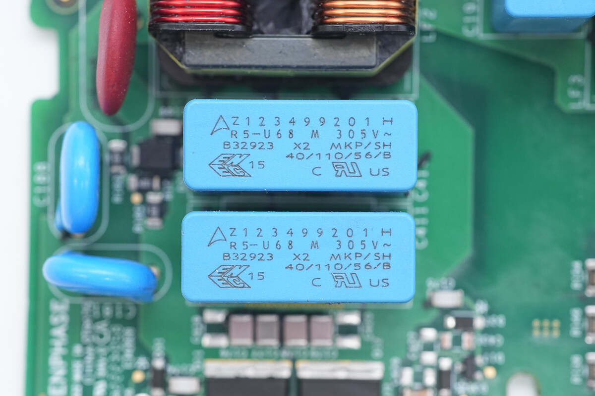
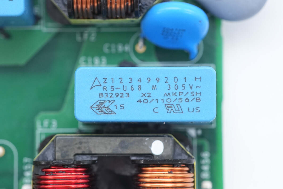
The two safety X2 capacitors are from TDK, each rated at 0.68μF.
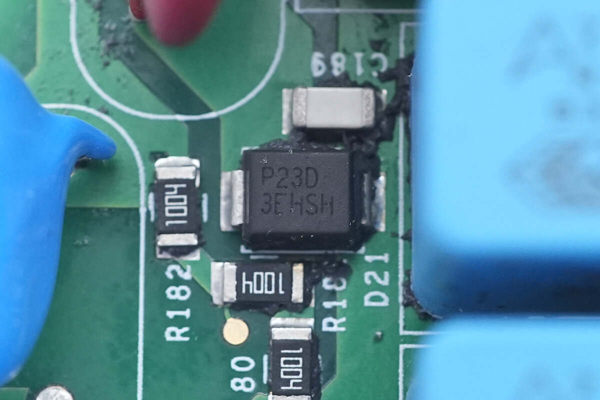
The gas discharge tube is marked with P23D, model P2300SD, used for overvoltage protection.

The varistor is from Littelfuse, marked with P175P10C, and used for absorbing overvoltage surges.
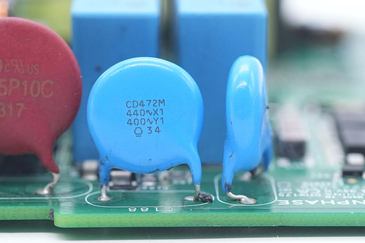
Close-up of two blue Y capacitors.
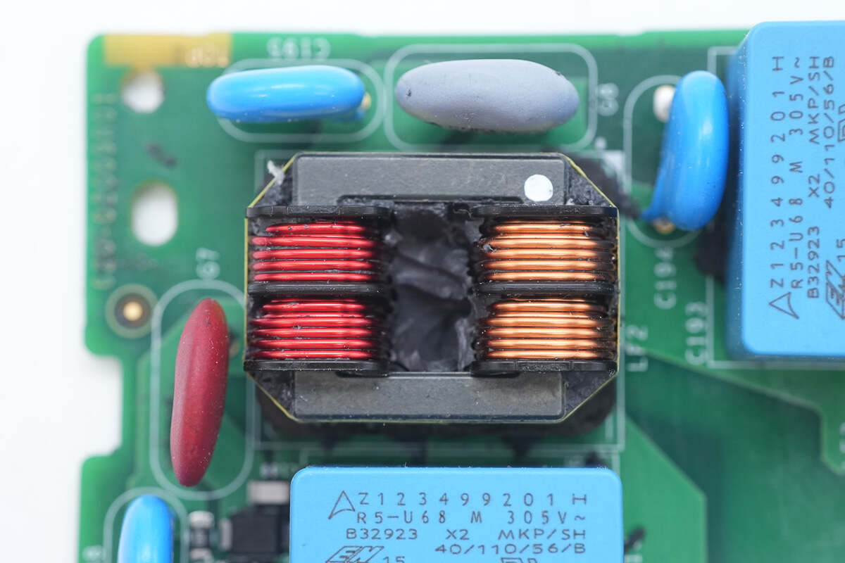
The common mode choke is wound with red and copper-colored enameled wires, and the magnetic core is insulated with wrapping tape.
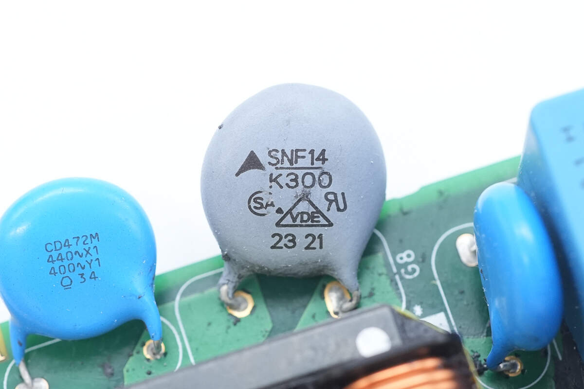
The varistor is from TDK, marked with SNF14K300, and used for absorbing overvoltage surges.
The safety X2 capacitor is rated at 0.68μF.
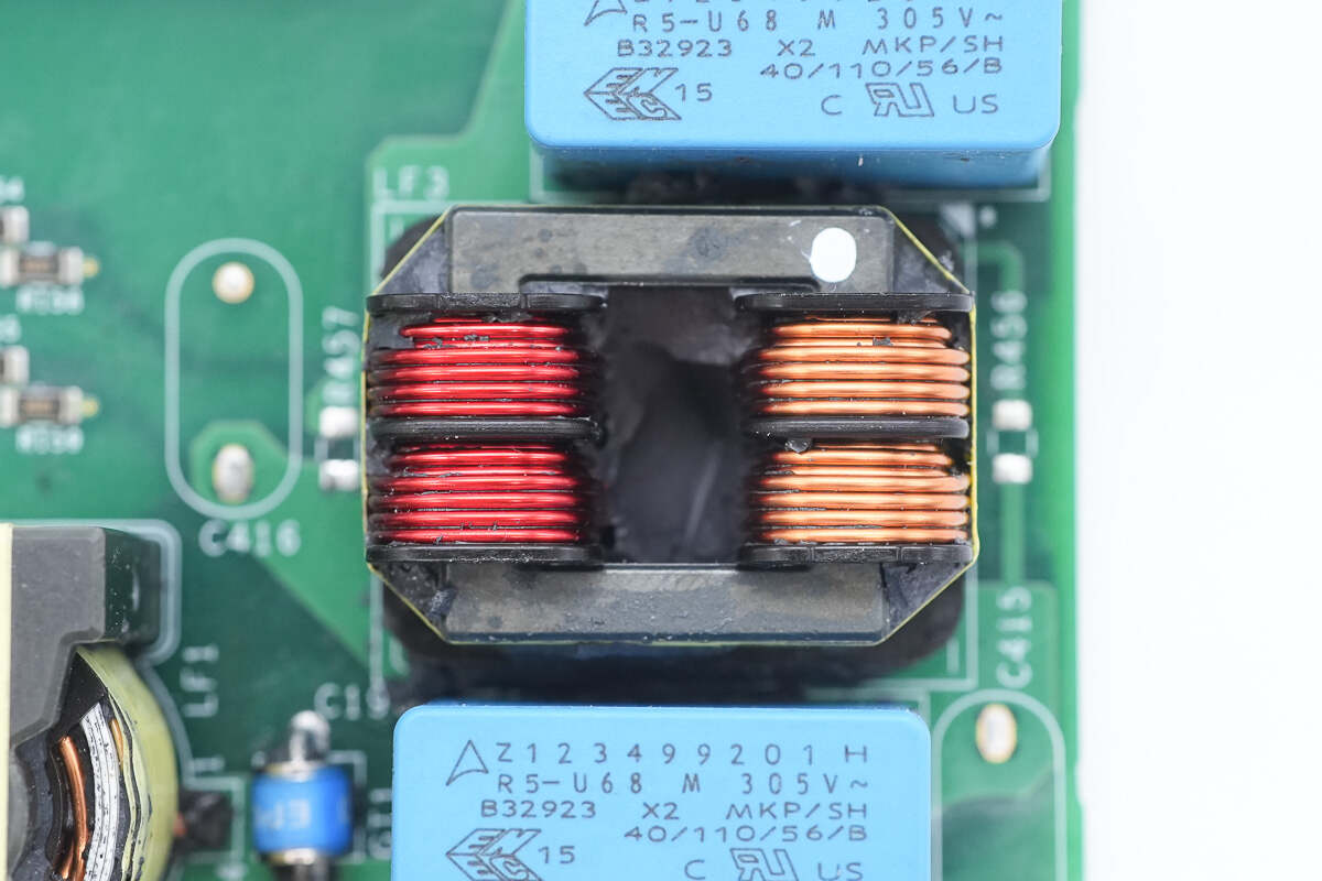
The other common mode choke has the same design.
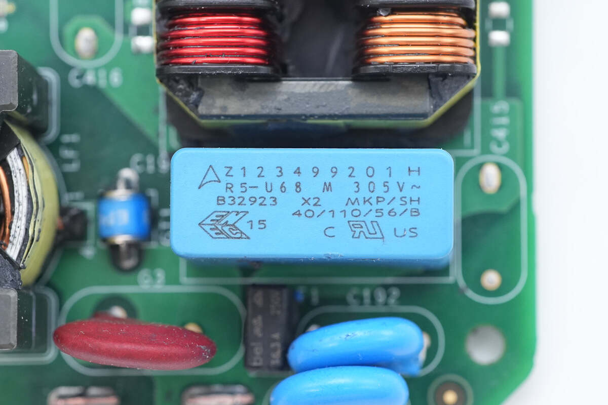
The other safety X2 capacitor has the same specifications.

Close-up of the blue Y capacitors.
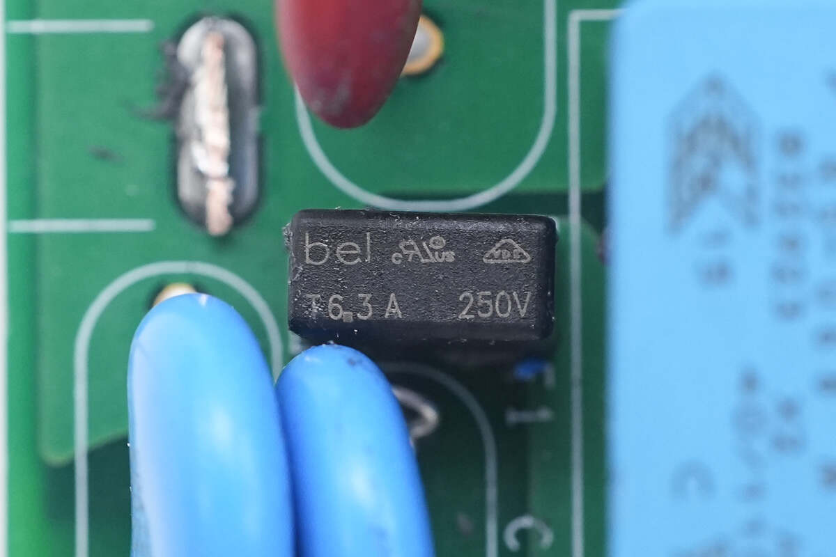
The fuse is from Belfuse, rated at 6.3A 250V.
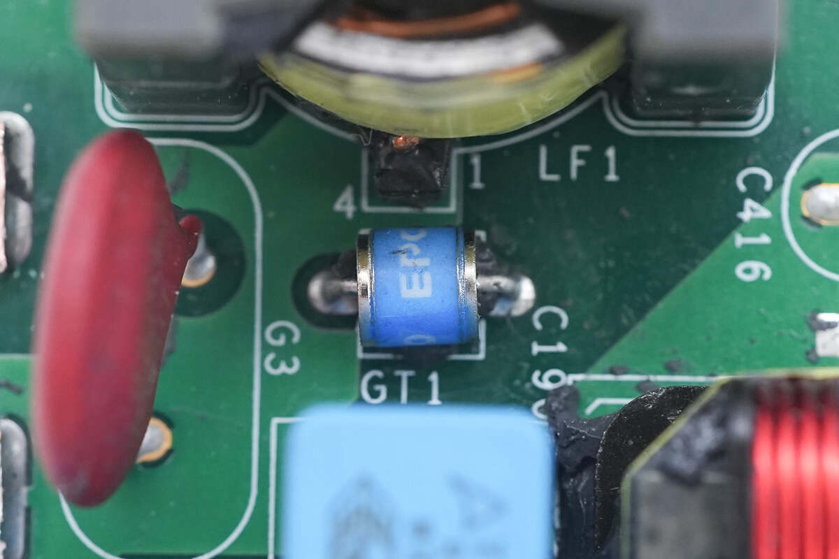
Close-up of the gas discharge tube used for overvoltage protection.
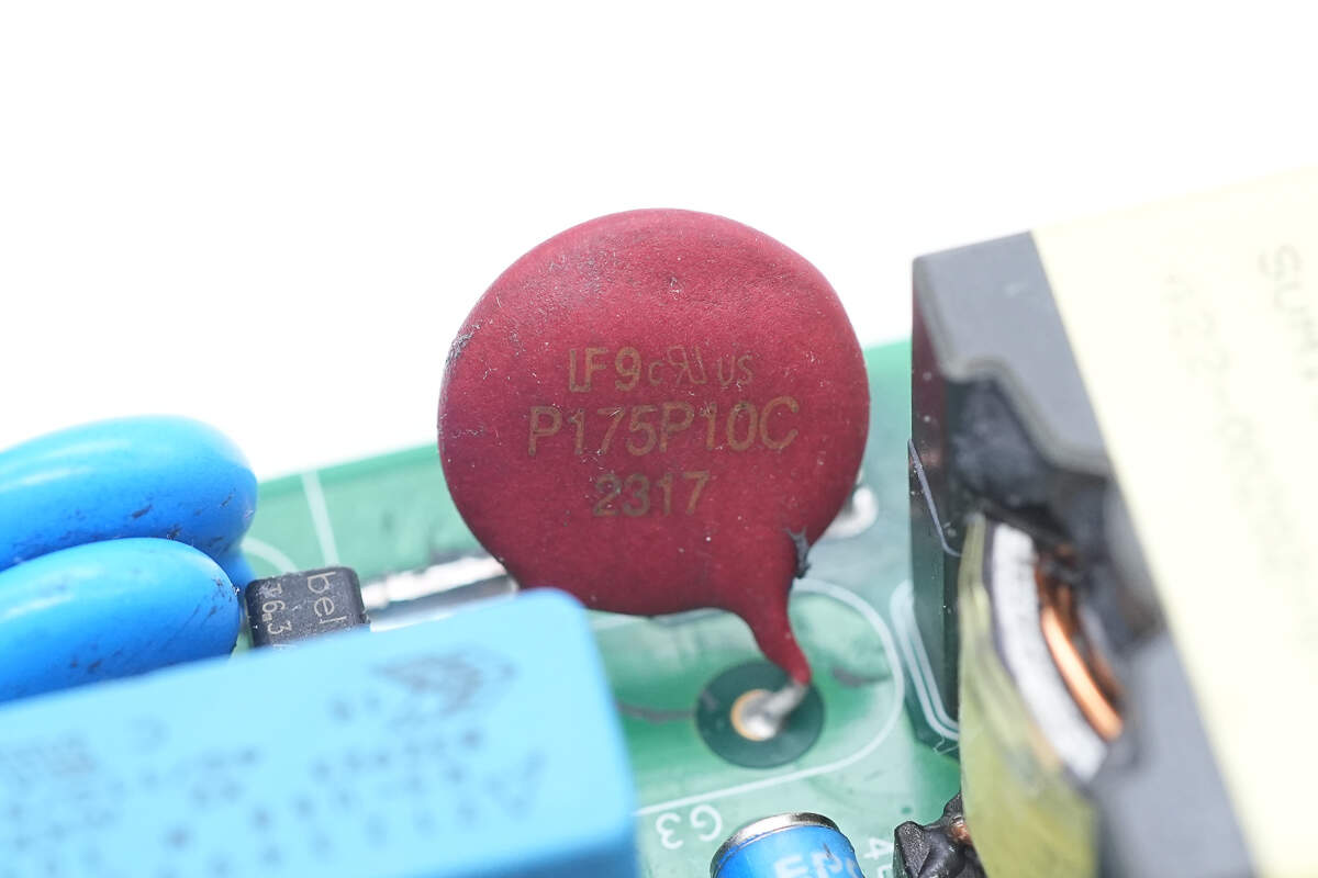
The Littelfuse varistor is marked with P175P10C.
Close-up of the coupling transformer.

Well, those are all components of the Enphase IQ8P 480W Microinverter.
Summary of ChargerLAB
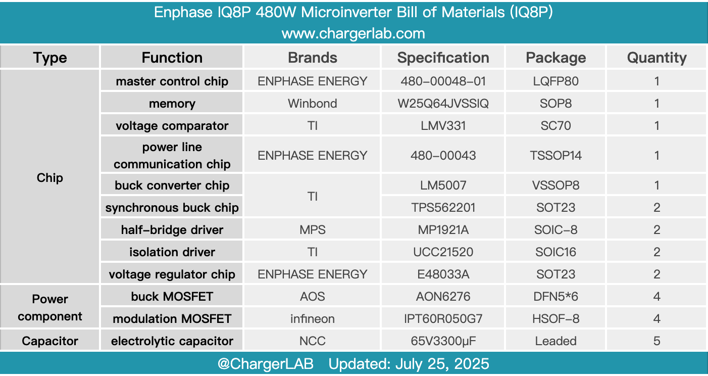
Here is the component list of the Enphase IQ8P 480W Microinverter for your convenience.
It features an engineered plastic enclosure with natural convection cooling, supporting an operating temperature range of -40 to 65°C. The output power is 480VA with an output voltage of 230V. It supports 60 to 78-cell PV modules, has a maximum input voltage of 65V, supports peak power tracking between 36 and 55V, and has a maximum short-circuit current of 25A.
After taking it apart, we found that the interior is filled with potting compound, providing excellent weather resistance. Thermal gel is applied to the PCB areas corresponding to heat-generating components, with an aluminum plate to enhance heat dissipation.
It uses ENPHASE custom master control and a power line communication chip. The boost stage employs MPS half-bridge drivers paired with AOS MOSFETs, while the output modulation utilizes TI isolation drivers combined with Infineon MOSFETs. NCC electrolytic capacitors are used for filtering. All components are sourced from internationally renowned brands, and the sealed design ensures reliable operation in harsh outdoor environments.
Related Articles:
1. Teardown of Xiaomi 33W 5000mAh 3-in-1 Power Bank (NPB0533)
2. Teardown of 90W GaN Charger for Xiaomi 15 Pro (MDY-14-EC)
3. Teardown of CUKTECH 67W CP6 GaN Charger (AD653W)