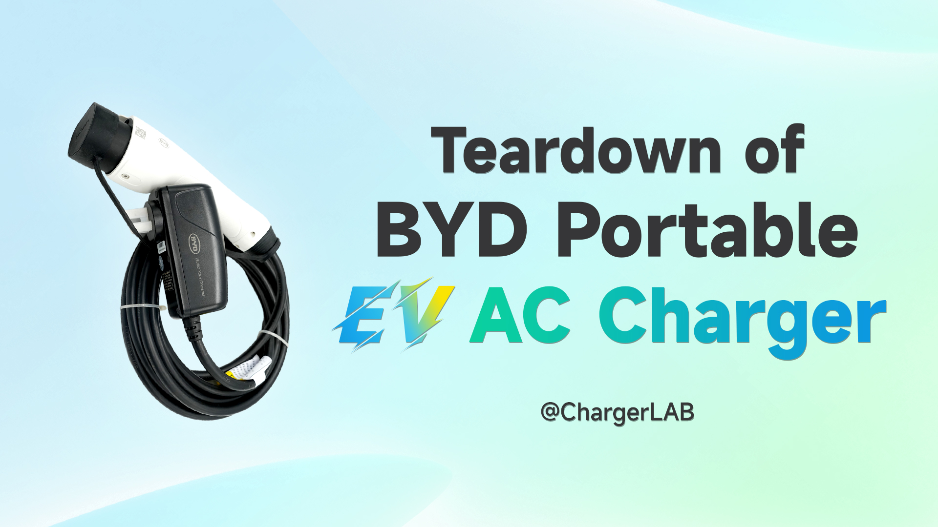
Introduction
CUKTECH has recently introduced a 90W mini GaN charger. Despite its compact, portable form factor and refined design, it offers a versatile port configuration with two USB-C ports and one USB-A port. The charger supports Xiaomi’s 90W HyperCharge technology, with both USB-C ports capable of delivering up to 65W PD output. The USB-A port delivers up to 22.5W of output and supports multiple fast-charging protocols. Below, we take a closer look at the detailed design of the product.
Product Appearance
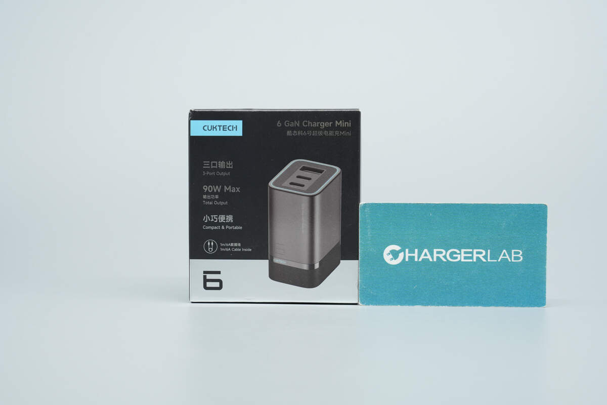
The front of the packaging displays the CUKTECH branding, product name, product appearance, and key selling points.
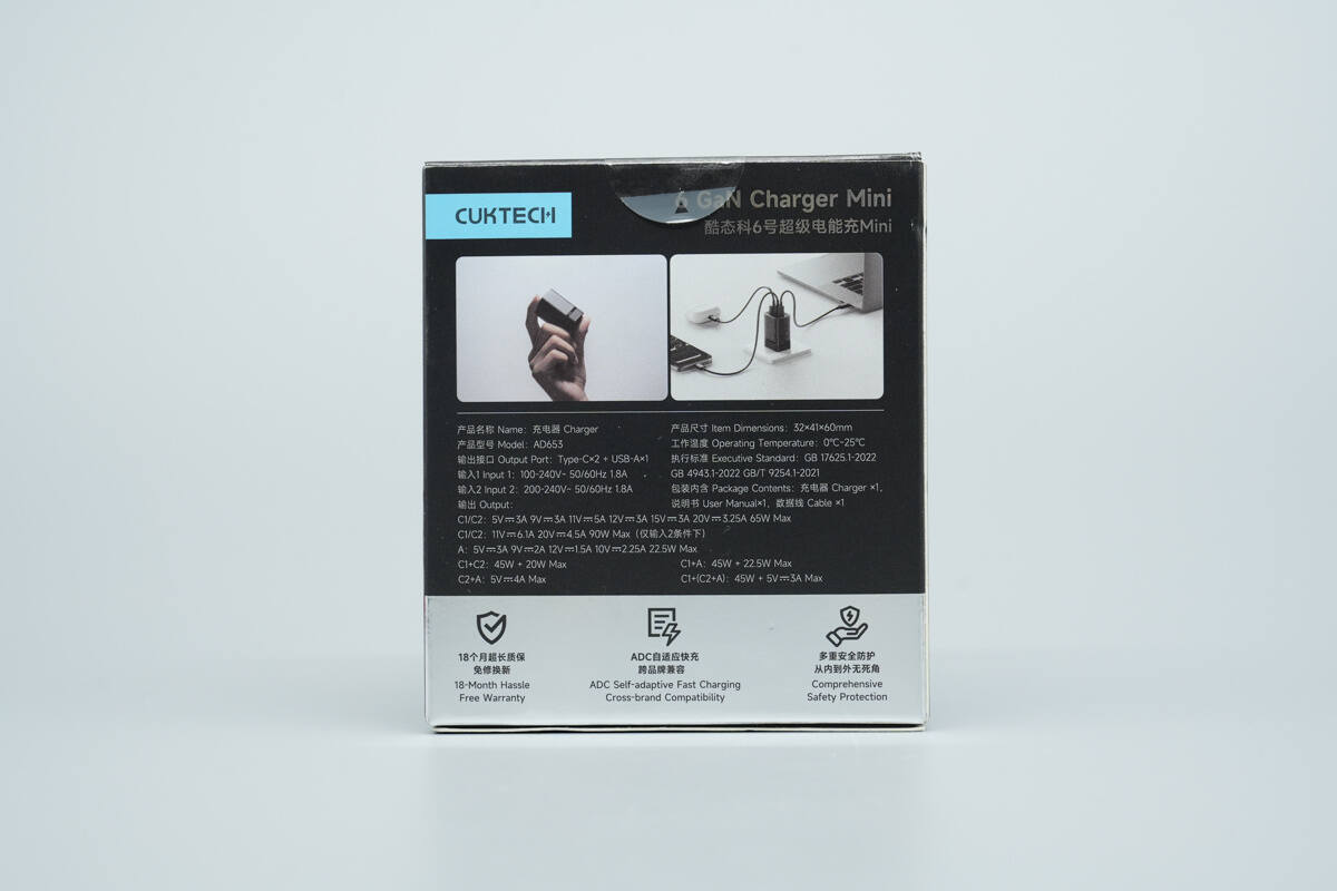
The back of the packaging features usage scenarios, specifications, and an overview of the product’s key advantages.
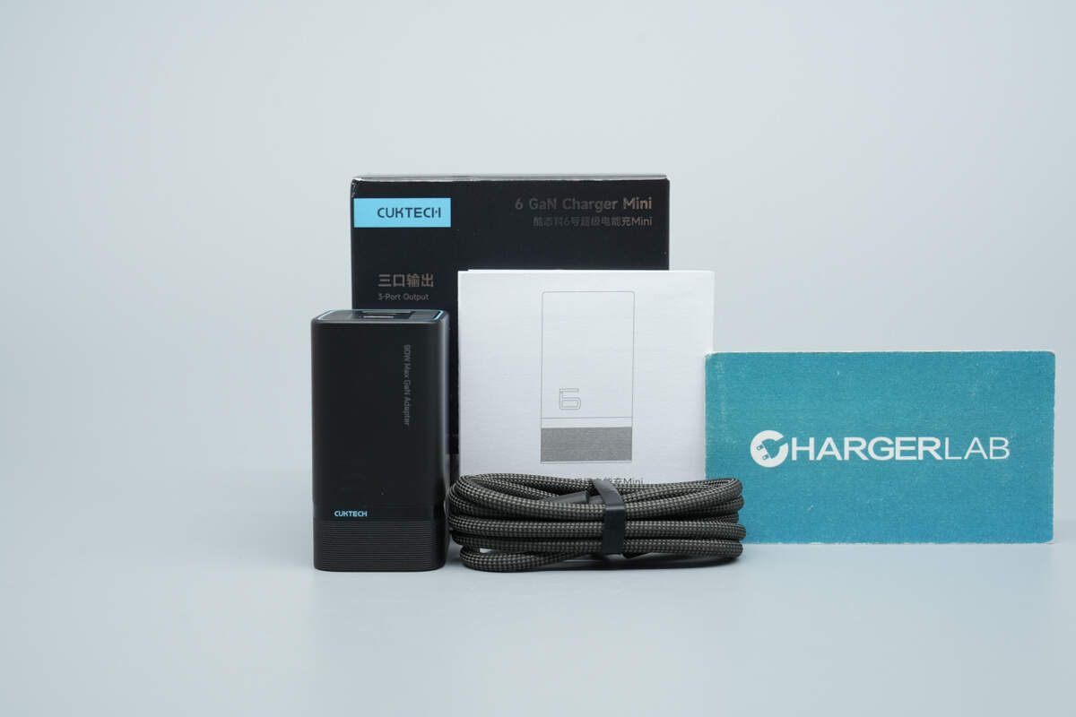
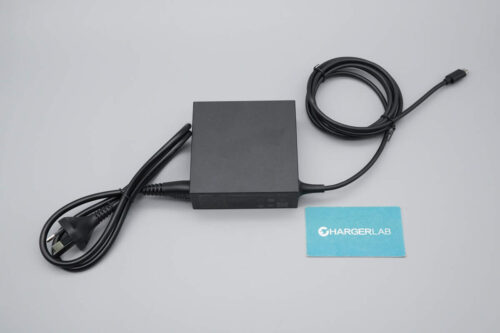
The package includes the charger, a charging cable, and a user manual.
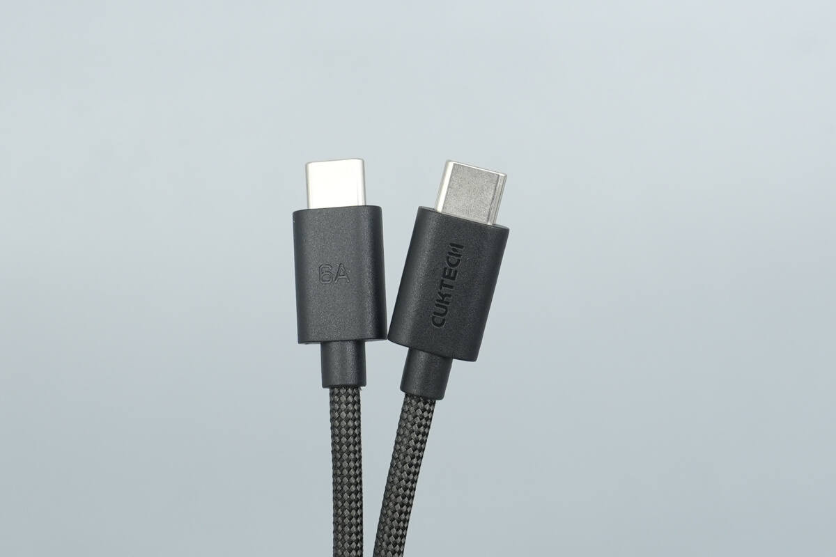
The included cable is a braided cable. Its connector housing features a matte finish for easier plugging and unplugging, and is marked with the CUKTECH branding and a “6A” designation.
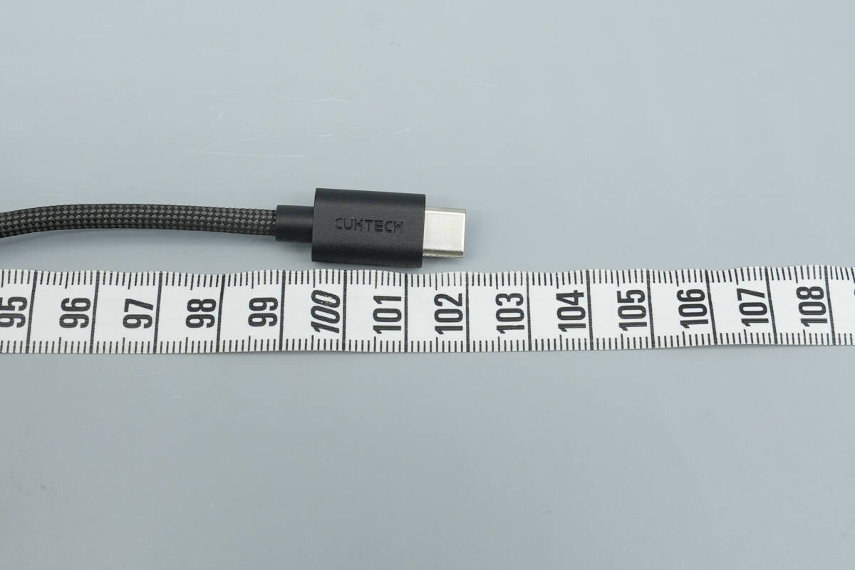
The length of the cable is about 102 cm (40.16 inches).
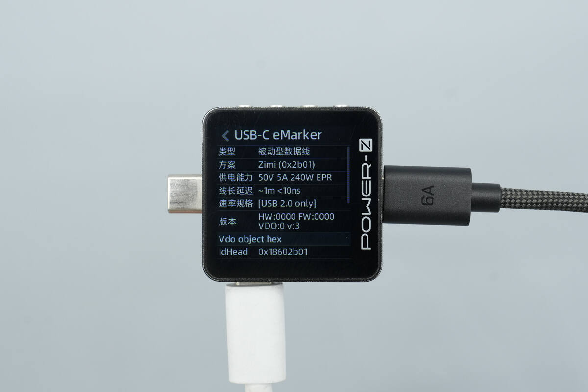
ChargerLAB POWER-Z KM003C indicates that the cable is equipped with an E-Marker chip, supporting power delivery up to 50V/5A and data transmission at USB 2.0 speeds.
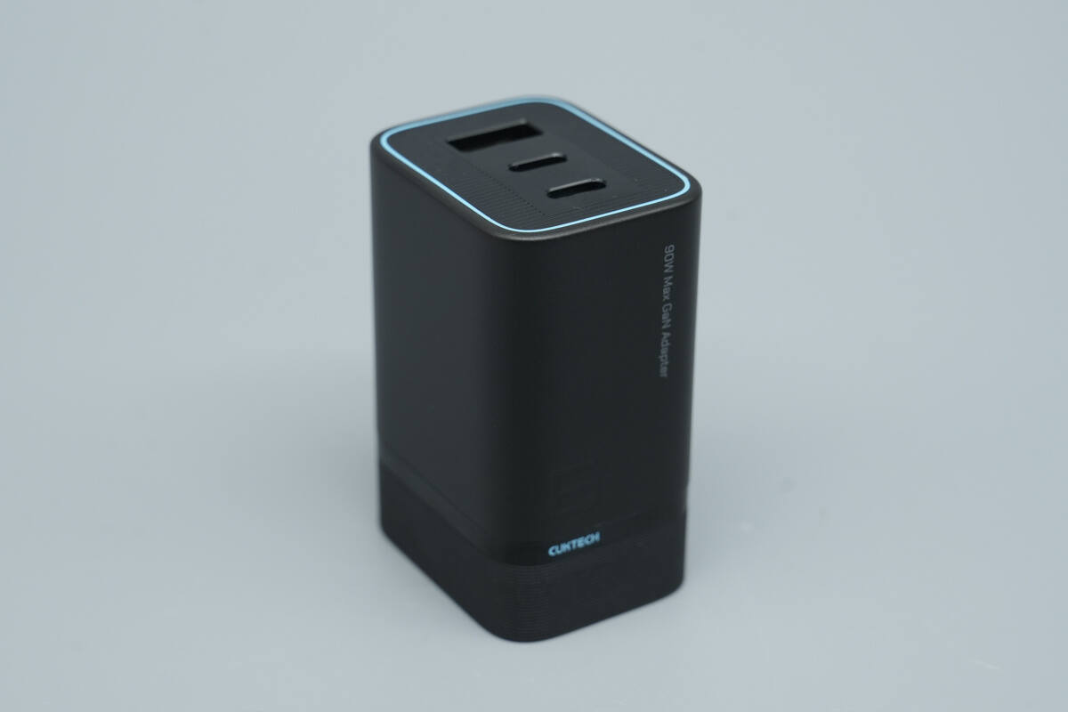
It adopts a cylindrical form factor with an all-black finish, accented by blue branding and a decorative ring.
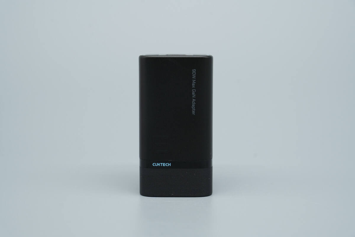
This side is printed with “CUKTECH” and “90W Max GaN Adapter.”
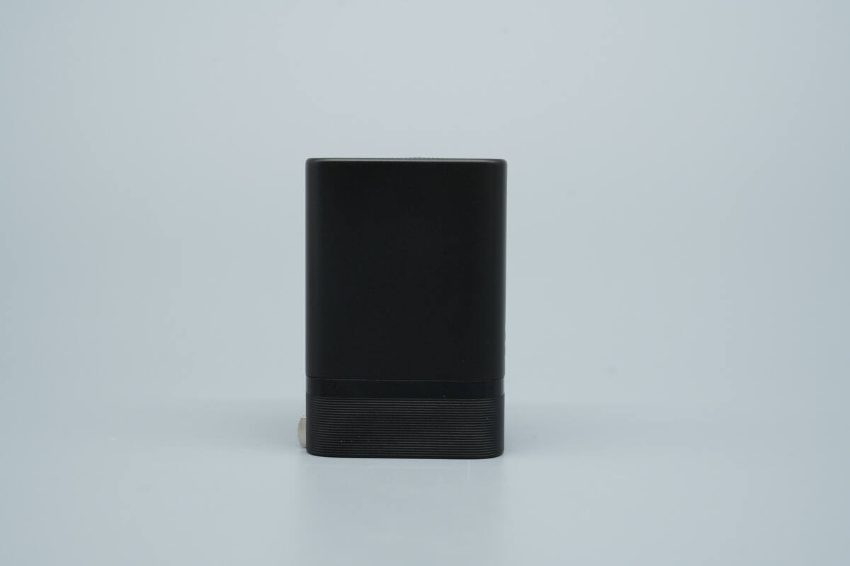
The back features a textured design with raised and recessed patterns.
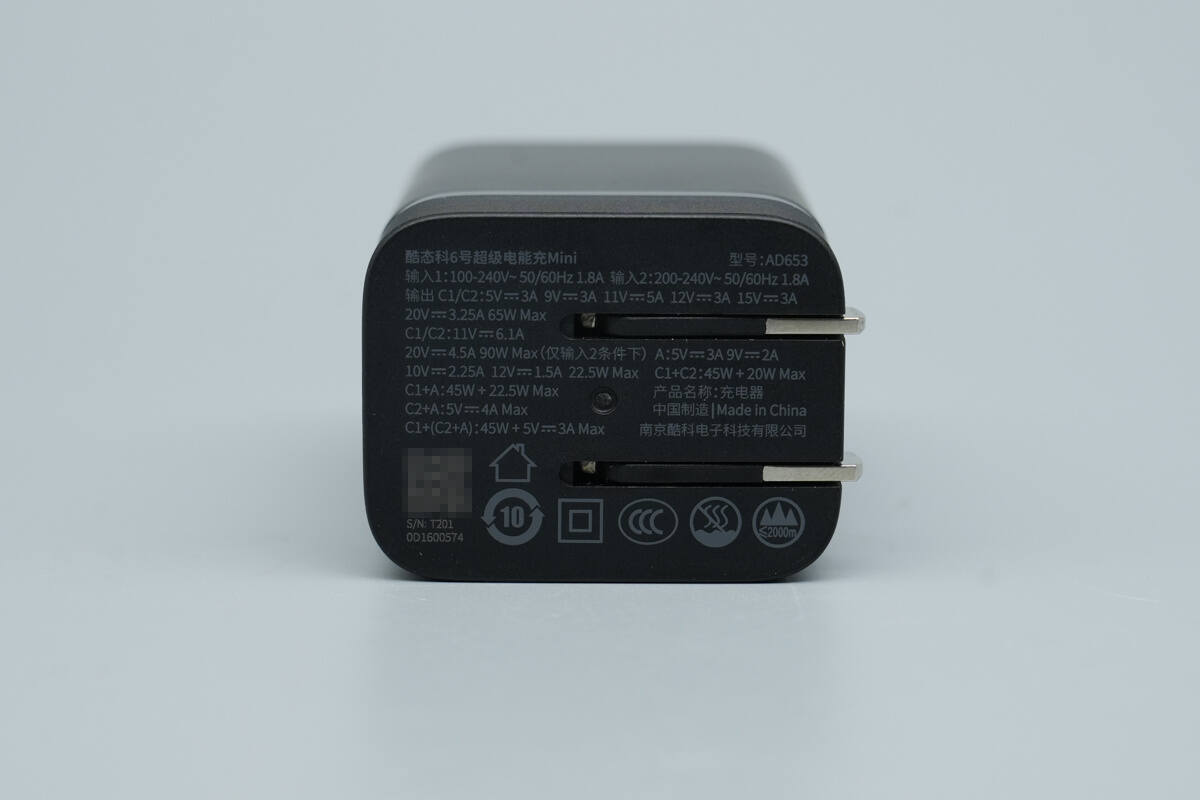
The input connector housing is printed with the specification information.
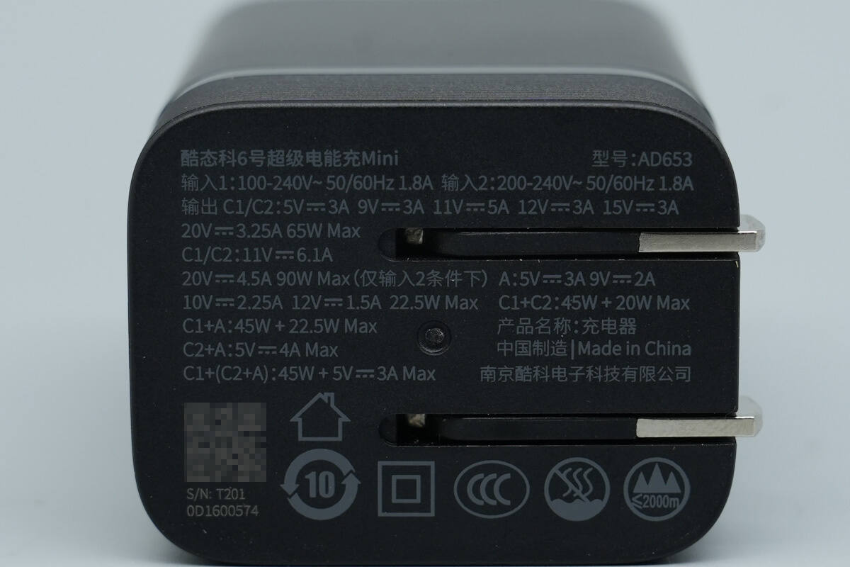
Model: AD653
Input 1: 100-240V~ 50/60Hz 1.8A
Input 2: 200-240V~ 50/60Hz 1.8A
Output:
C1/C2: 5V 3A, 9V 3A, 11V 5A, 12V 3A, 15V 3A, 20V 3.25A, 65W Max
C1/C2: 11V 6.1A, 20V 4.5A, 90W Max (only under Input 2 conditions)
A: 5V 3A, 9V 2A, 10V 2.25A, 12V 1.5A, 22.5W Max
C1 + C2: 45W + 20W Max
C1 + A: 45W + 22.5W Max
C2 + A: 5V 4A Max
C1 + (C2 + A): 45W + 5V 3A Max
The charger is CCC certified.
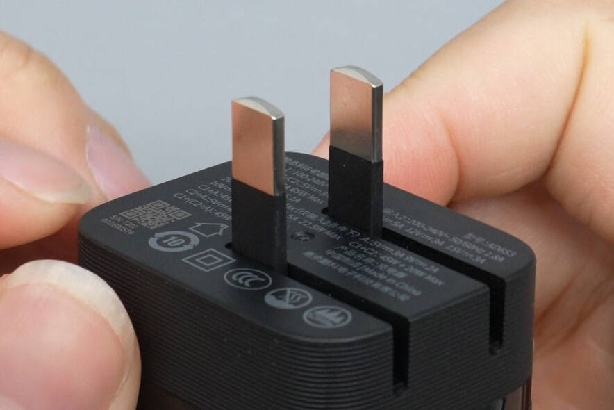
It is equipped with foldable plug pins.
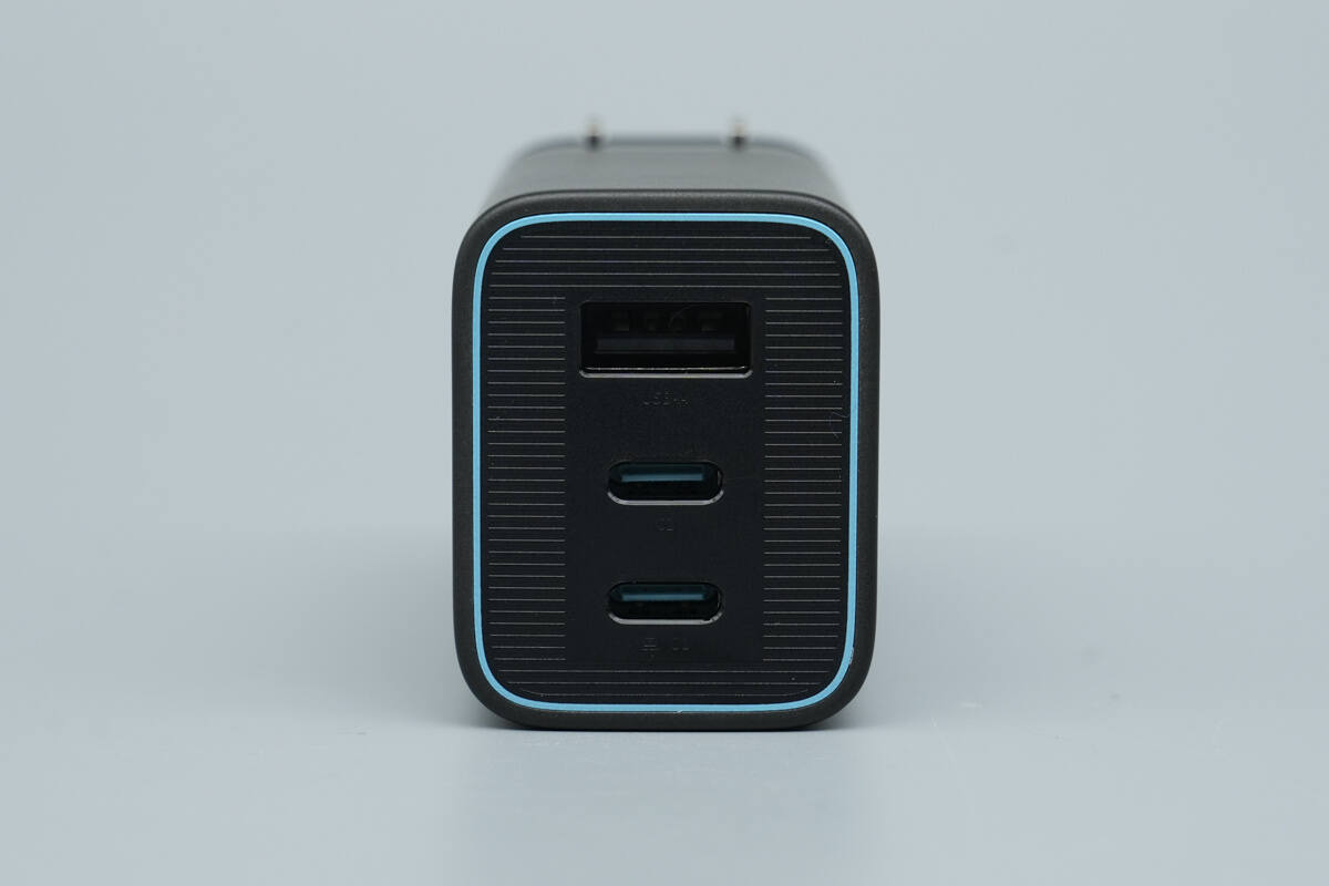
The top also features a textured surface and houses two USB-C ports and one USB-A port.
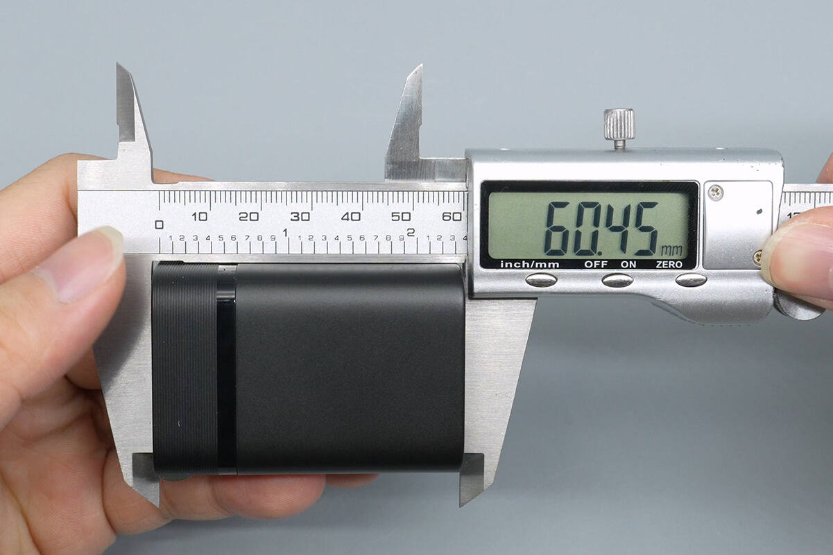
The length of the charger is about 60.45 mm (2.38 inches).
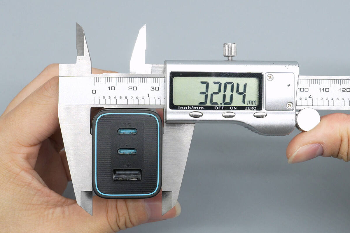
The width is about 32.04 mm (1.26 inches).
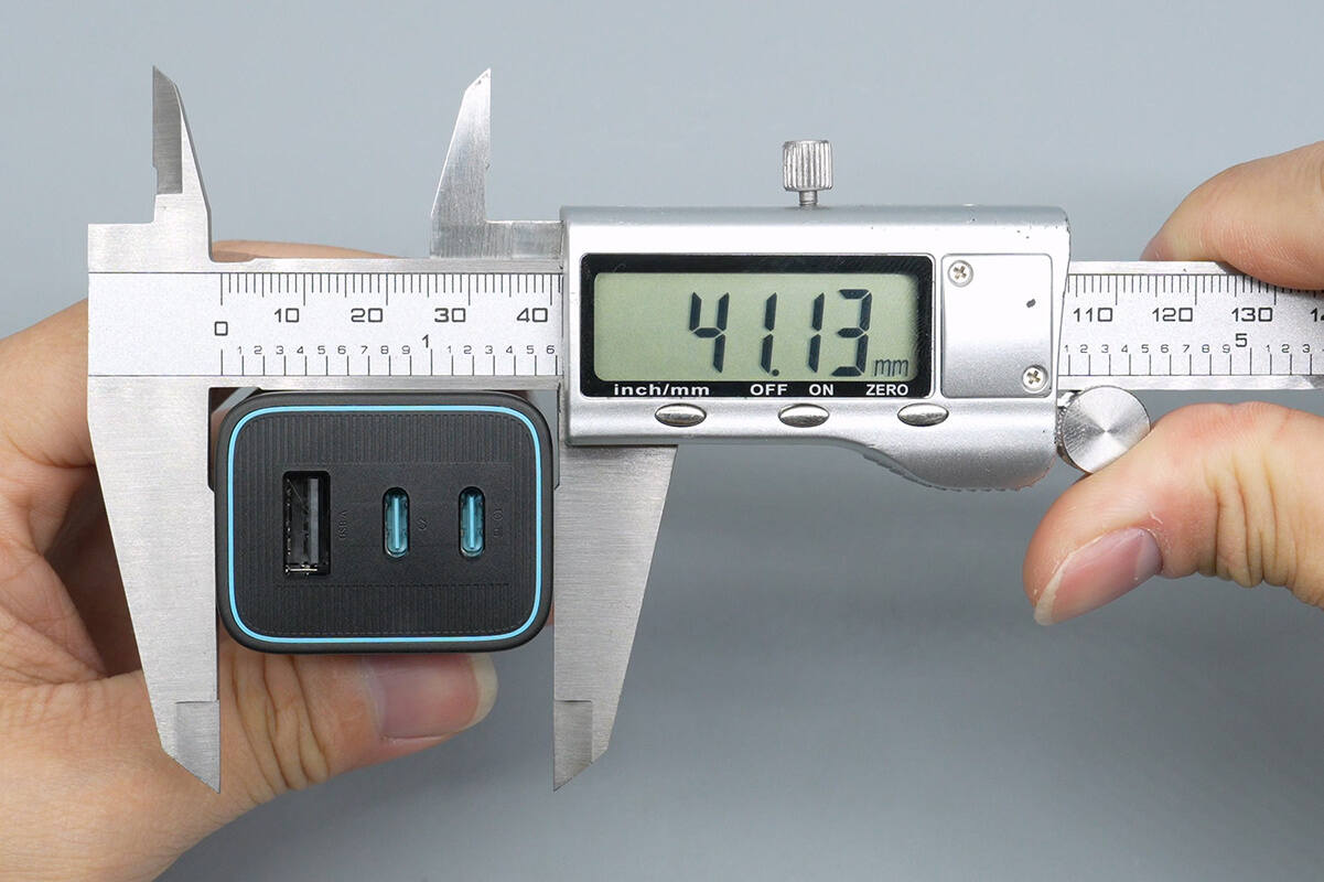
The thickness is about 41.13 mm (1.62 inches).
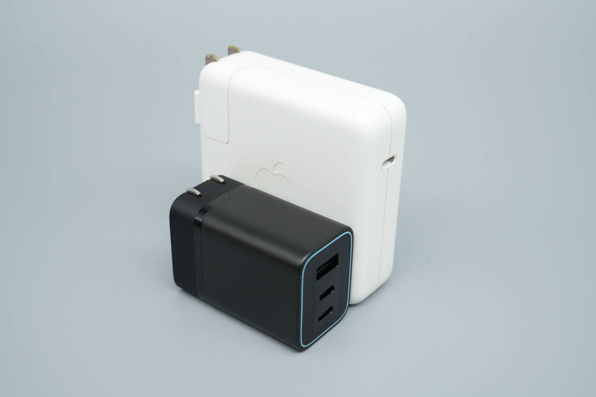
Its size is slightly smaller than that of the Apple 90W charger.
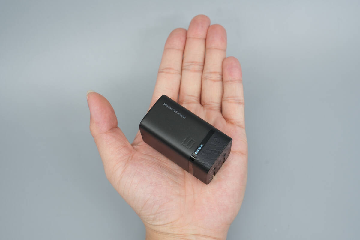
That's how big it is on the hand.
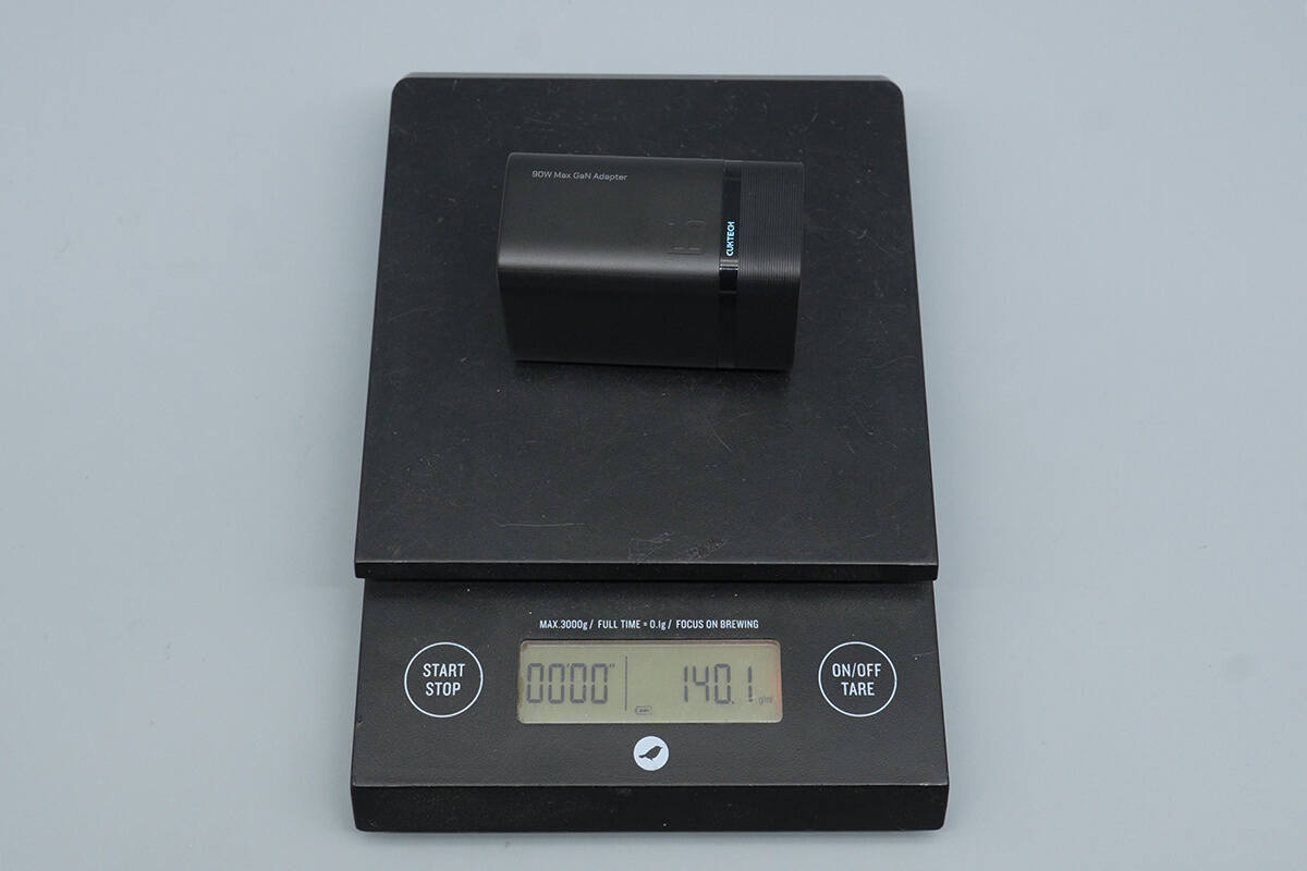
The weight is about 140 g (4.94 oz).
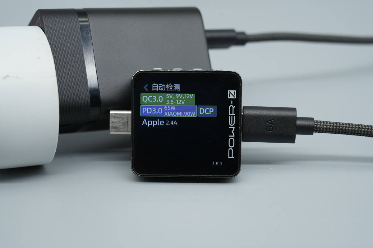
ChargerLAB POWER-Z KM003C shows that the USB-C1 port supports QC3.0, PD3.0, DCP, Apple 2.4A charging protocols, as well as Xiaomi’s 90W proprietary fast-charging protocol.
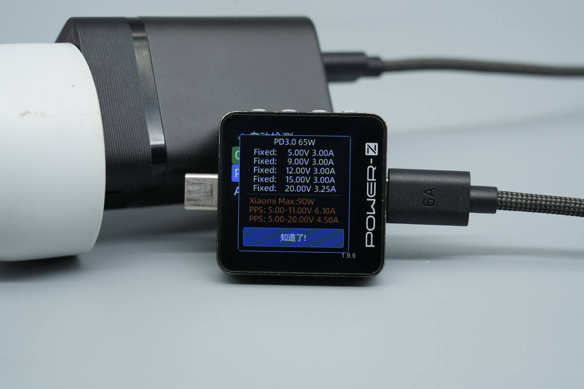
It features five fixed PDOs of 5V 3A, 9V 3A, 12V 3A, 15V 3A, and 20V 3.25A. It also supports two Xiaomi proprietary voltage levels: 5–11V 6.1A and 5–20V 4.5A.
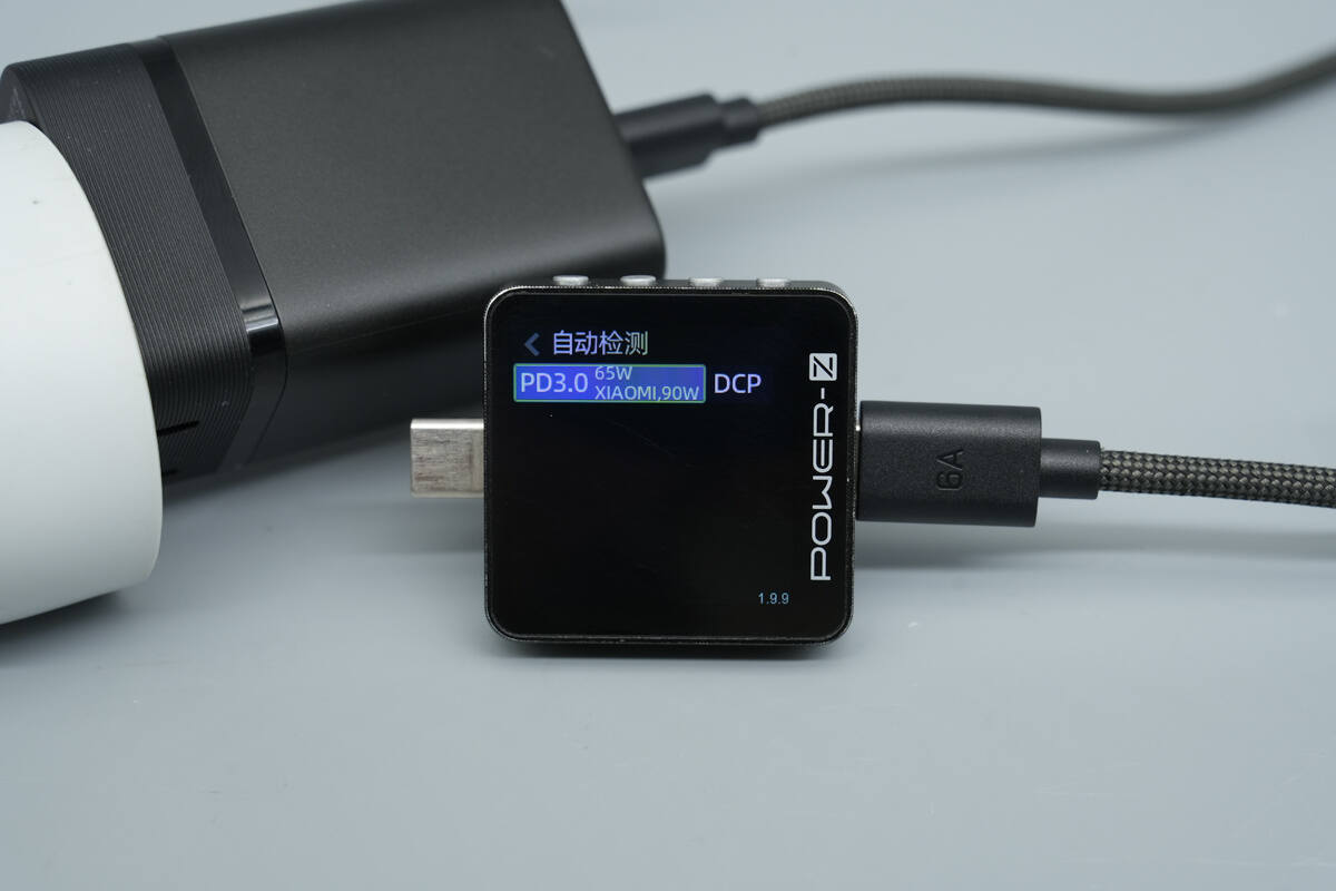
The USB-C2 port supports PD3.0 and DCP charging protocols, as well as Xiaomi’s 90W proprietary fast-charging protocol.
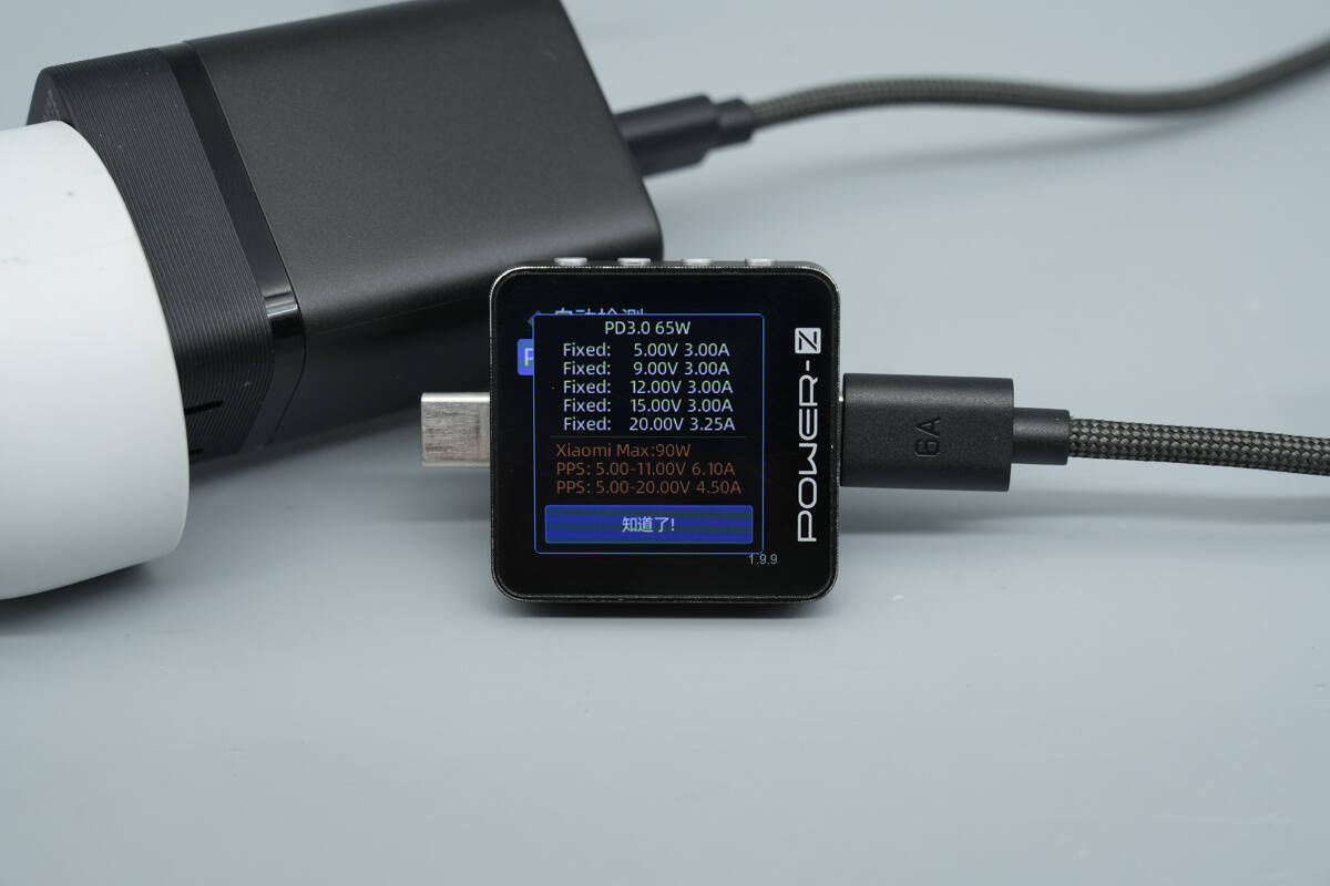
It features five fixed PDOs of 5V 3A, 9V 3A, 12V 3A, 15V 3A, and 20V 3.25A. It also supports two Xiaomi proprietary voltage levels: 5–11V 6.1A and 5–20V 4.5A.
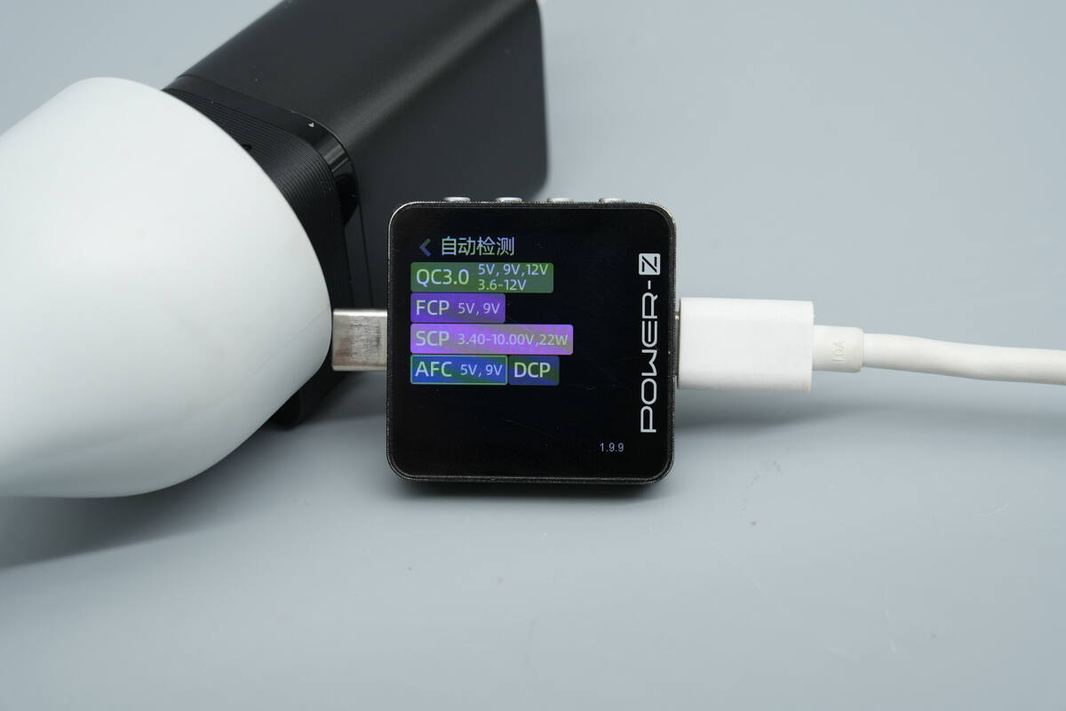
The USB-A port supports C3.0, FCP, SCP, AFC, and DCP charging protocols.
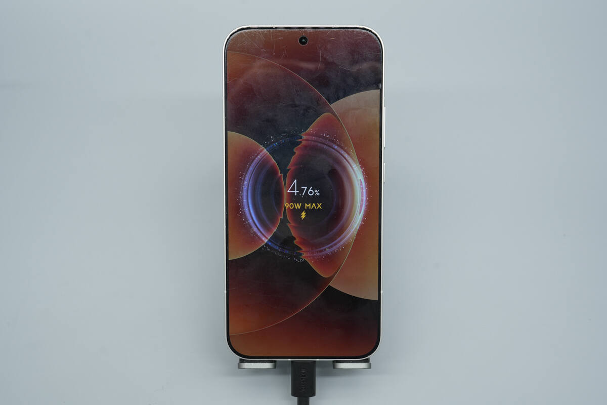
Using the USB-C1 port to charge the Xiaomi 17 Pro Max, the device successfully activated Xiaomi’s 90W HyperCharge fast-charging.
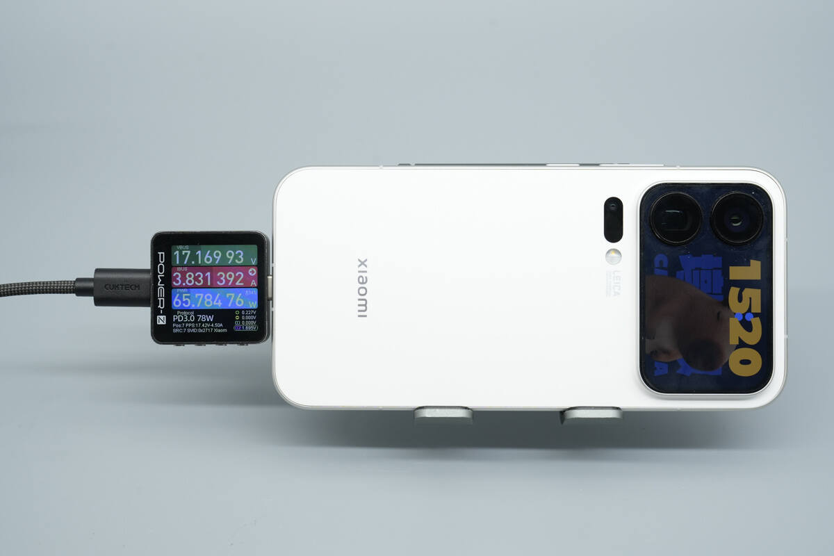
When the charging power reaches a stable state, it measures about 65.78W.
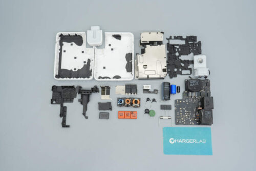
Teardown
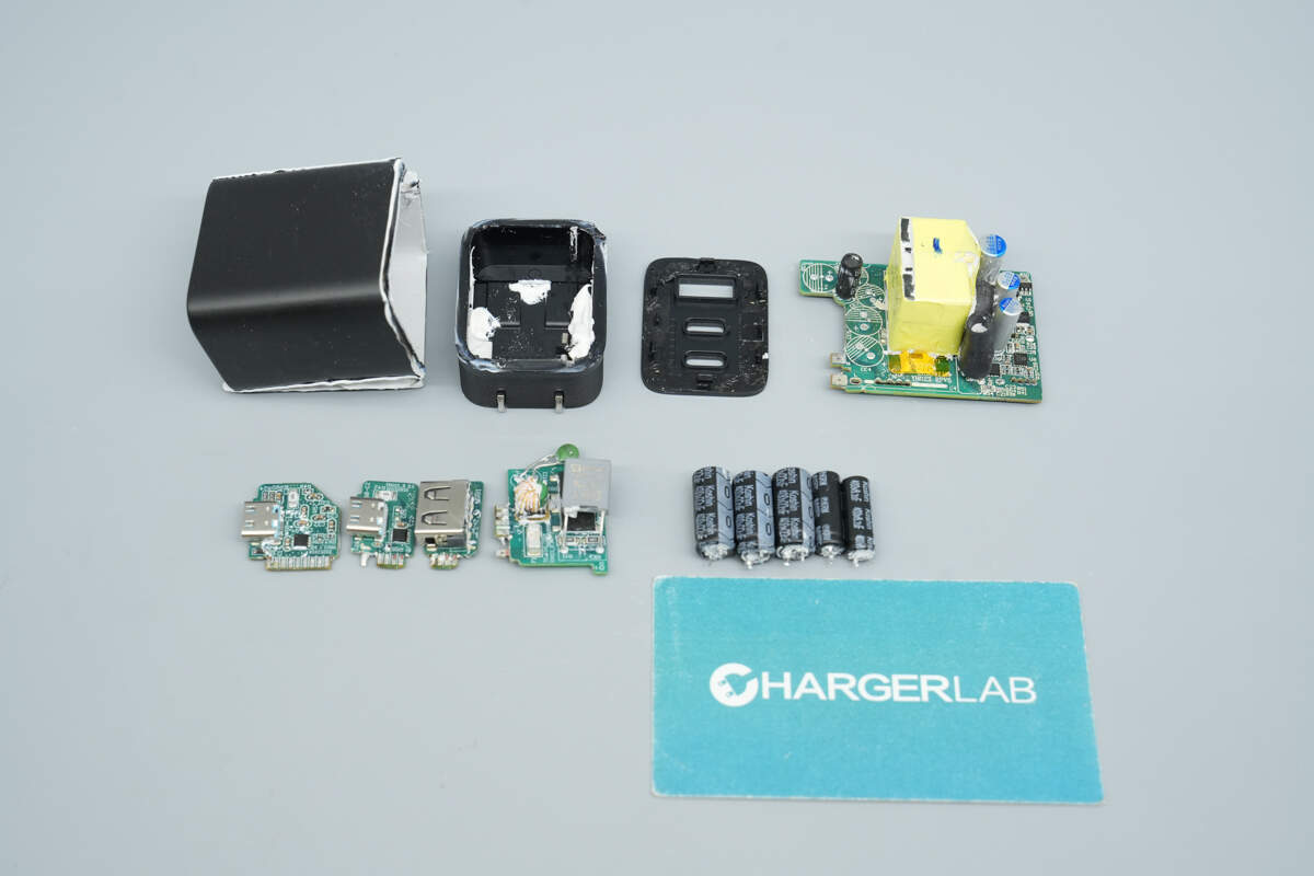
Next, let's take it apart to see its internal components and structure.
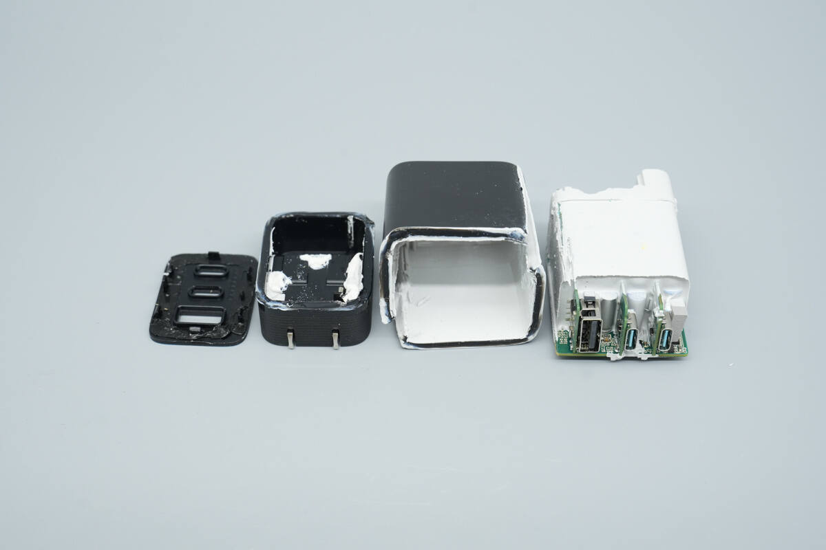
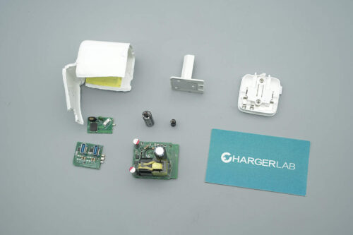
Cut open the casing to extract the PCBA module. The input section uses a contact-based power design, and the interior of the housing is lined with aerogel.
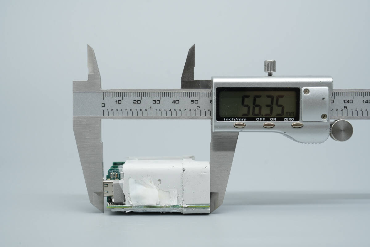
The length of the PCBA module is about 56.35 mm (2.22 inches).
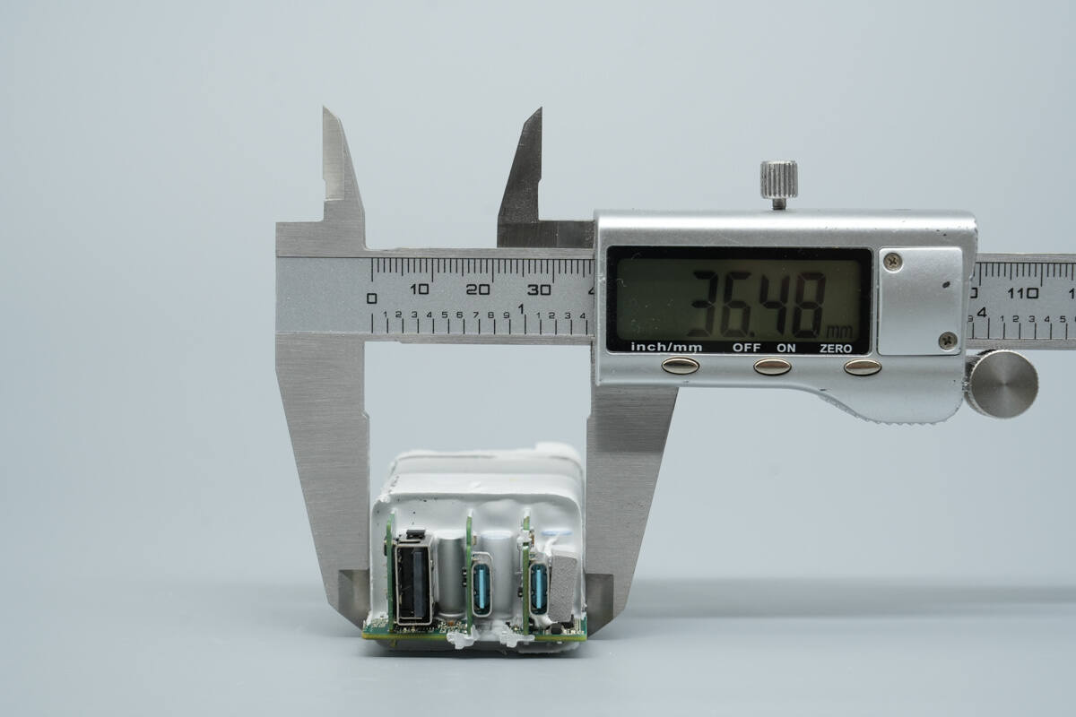
The width is about 36.48 mm (1.44 inches).
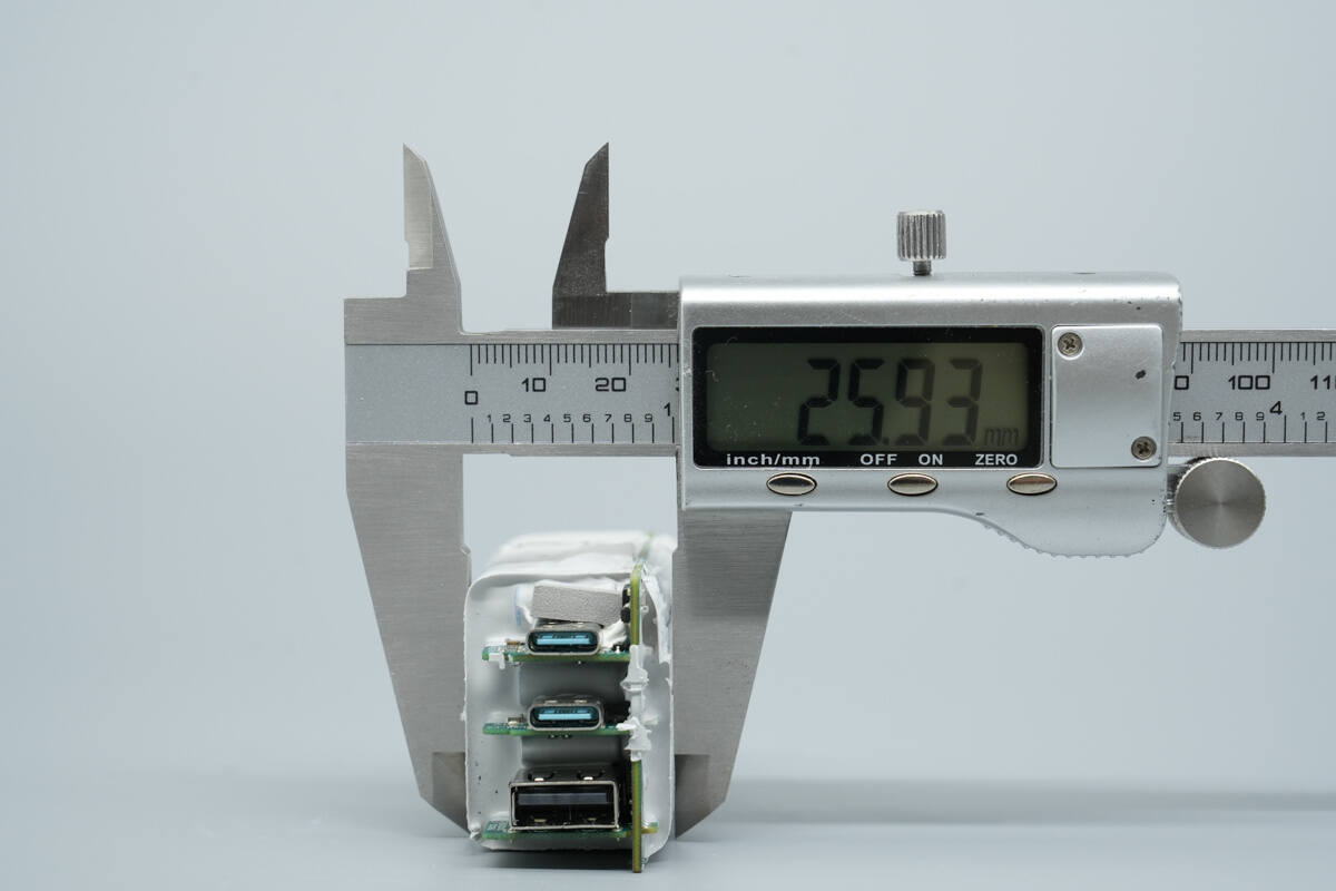
The thickness is about 25.93 mm (1.021 inches).
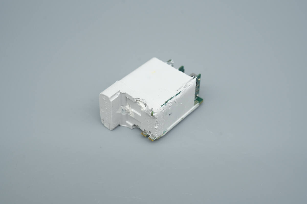
The PCBA module is encapsulated with adhesive to enhance overall durability and heat dissipation performance.
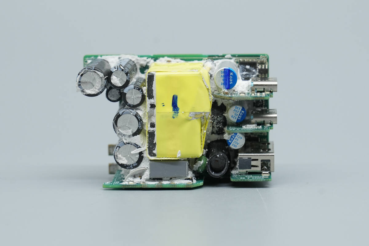
After removing the thermal adhesive, the front of the PCBA module reveals a compact component layout. Small PCBs are soldered on the sides and output terminals, and the buck inductors are insulated with heat-shrink tubing.
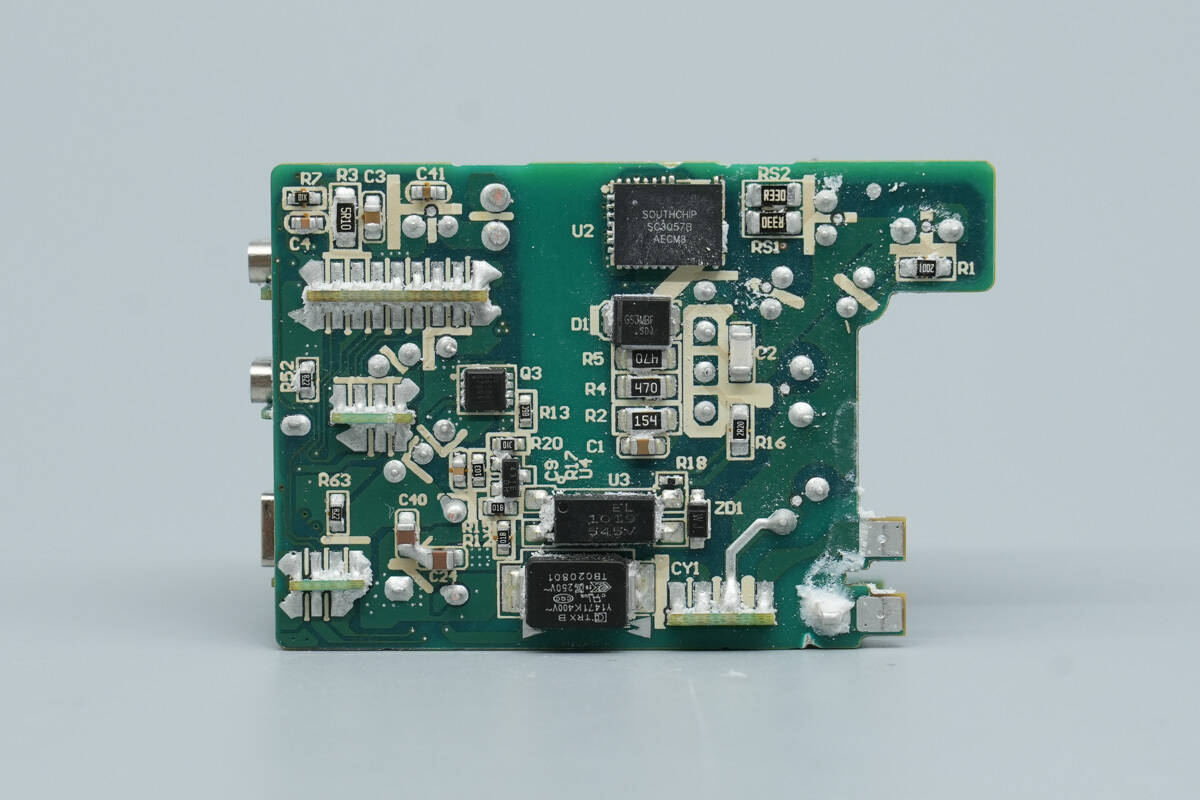
On the back, there is the master control chip, an optocoupler, an SMD Y capacitor, and VBUS MOSFETs.
At the front end of the PCBA module, there are high-voltage filter electrolytic capacitors and an I-shaped inductor, with an input PCB located on the right side.
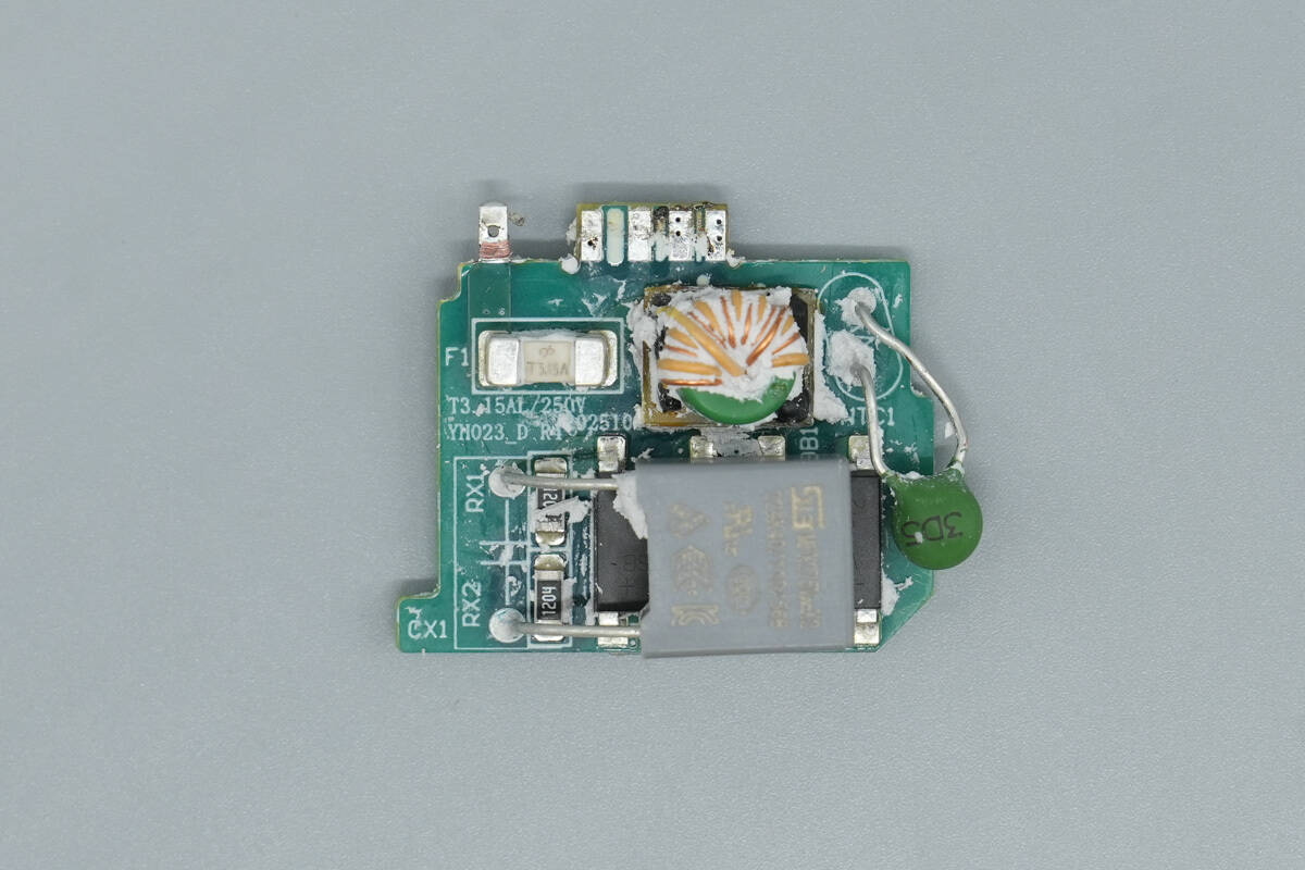
After removing the small PCB, the front side reveals an SMD fuse, a common mode choke, a safety X2 capacitor, an NTC thermistor, and bridge rectifiers.
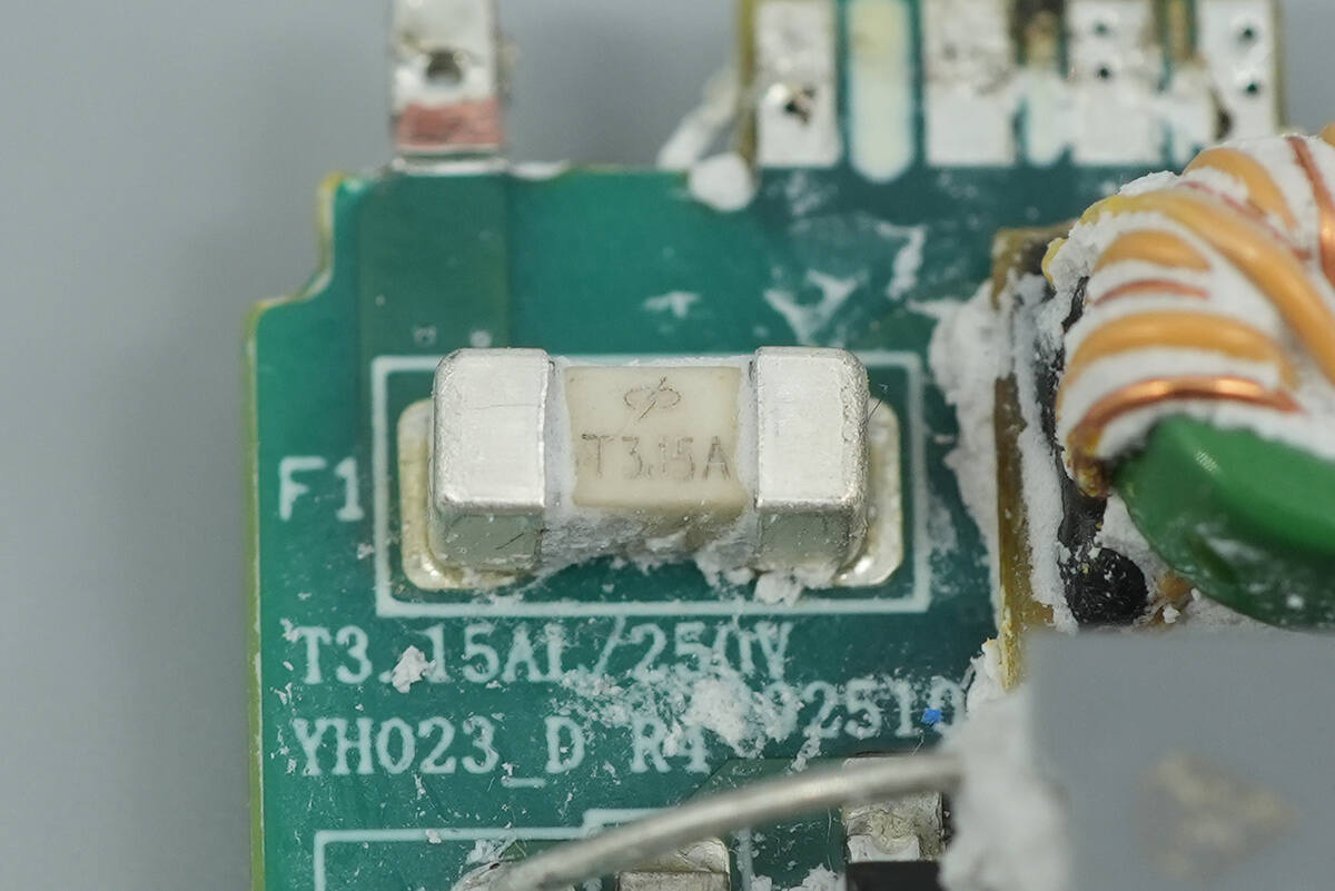
The SMD fuse is rated at 3.15 A.
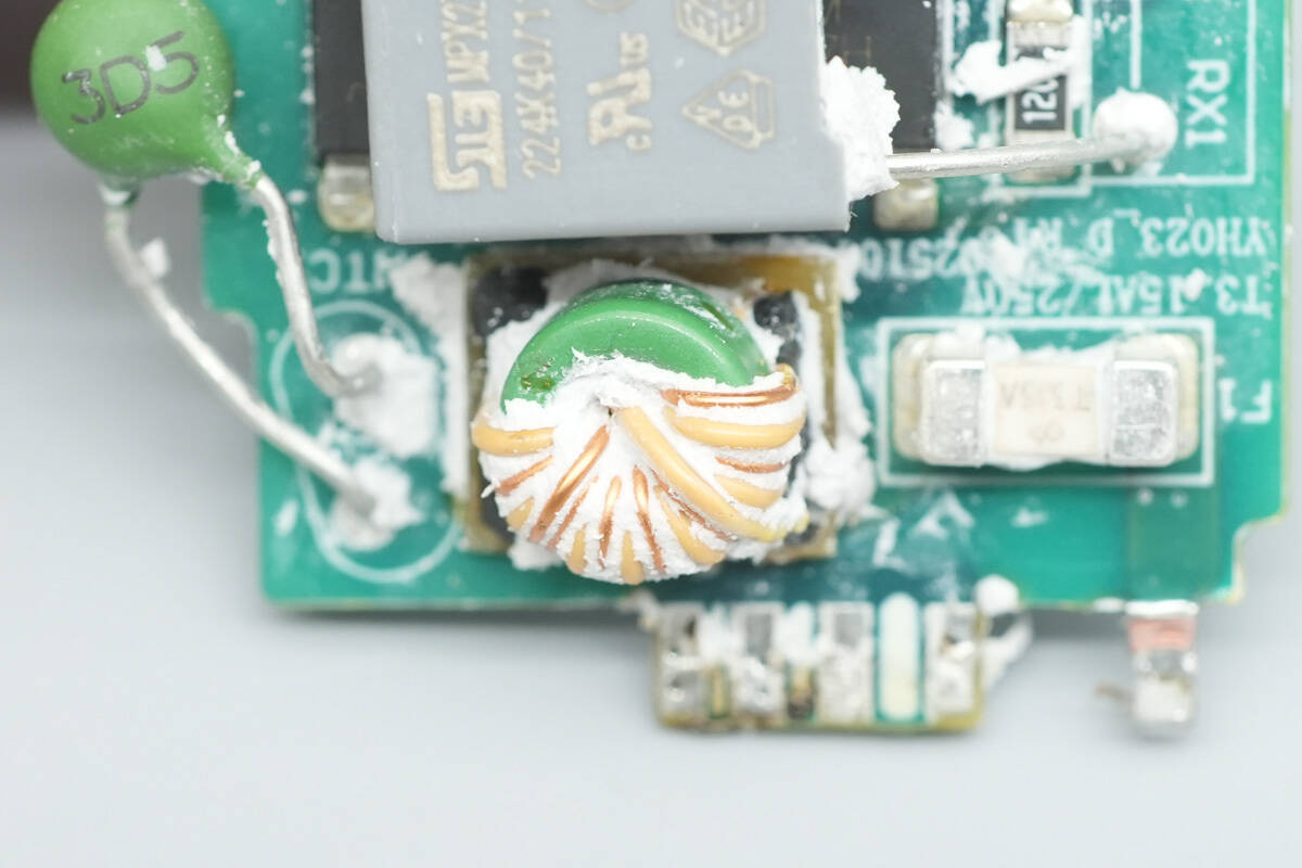
The common mode choke is dual-wound and is used to suppress EMI.
The NTC thermistor is used to suppress inrush current at power-on.
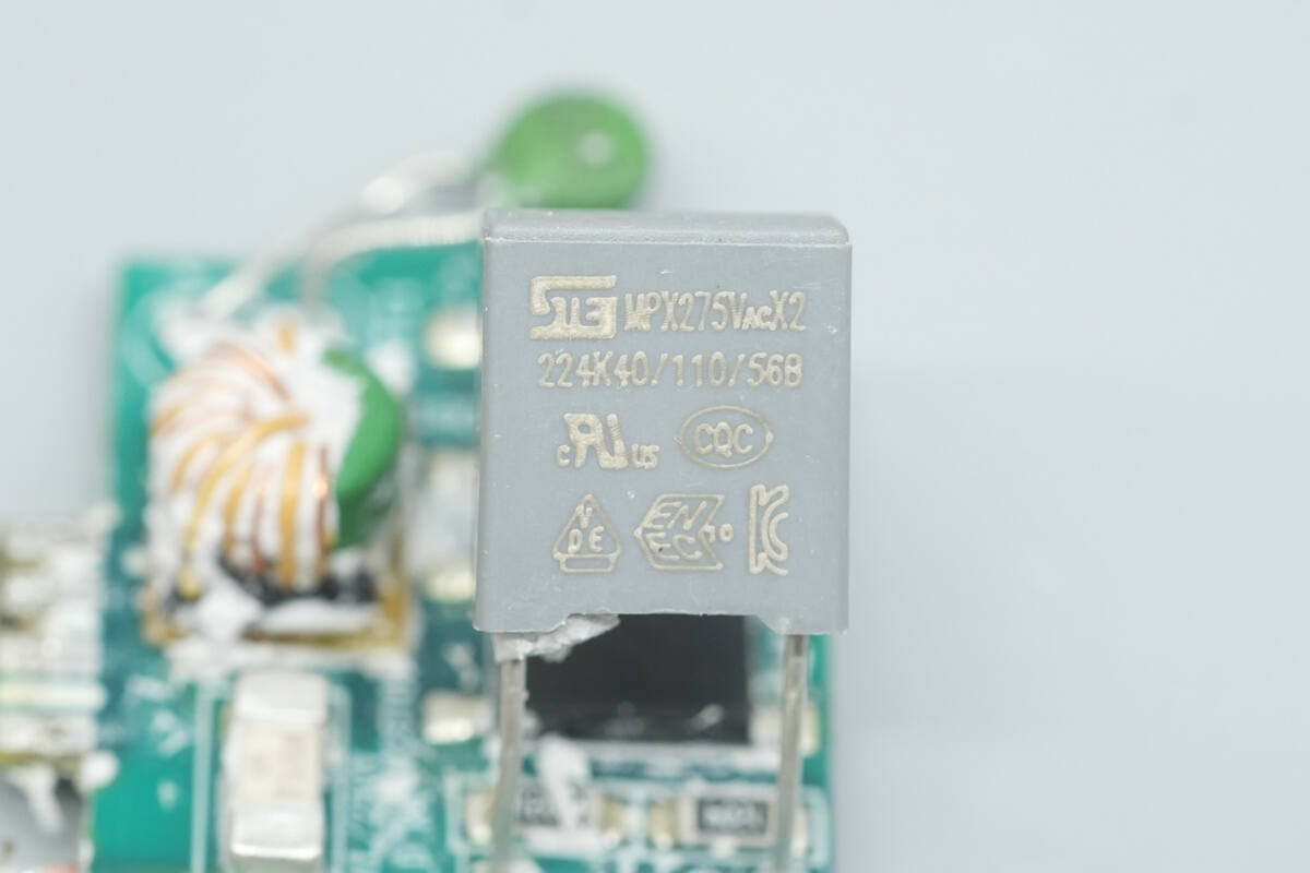
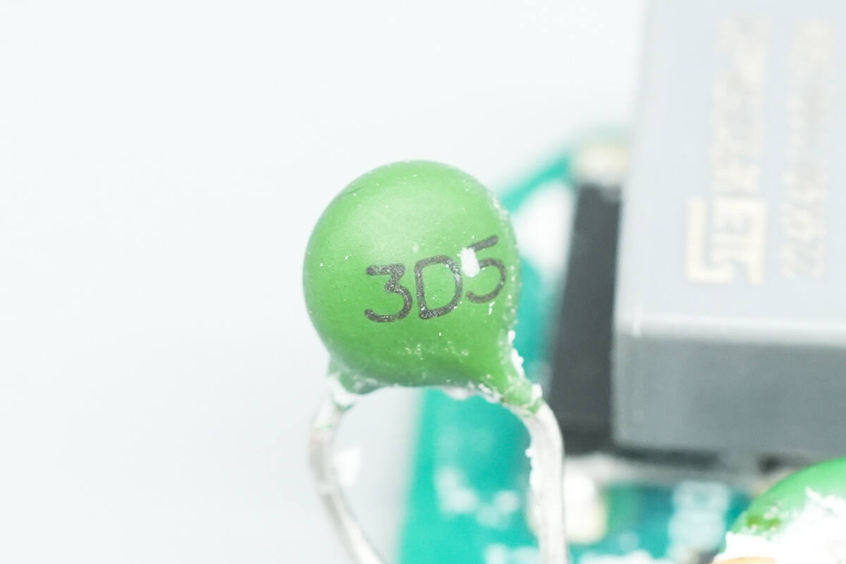
The safety X2 capacitor is from STE and has a capacitance of 0.22 μF.
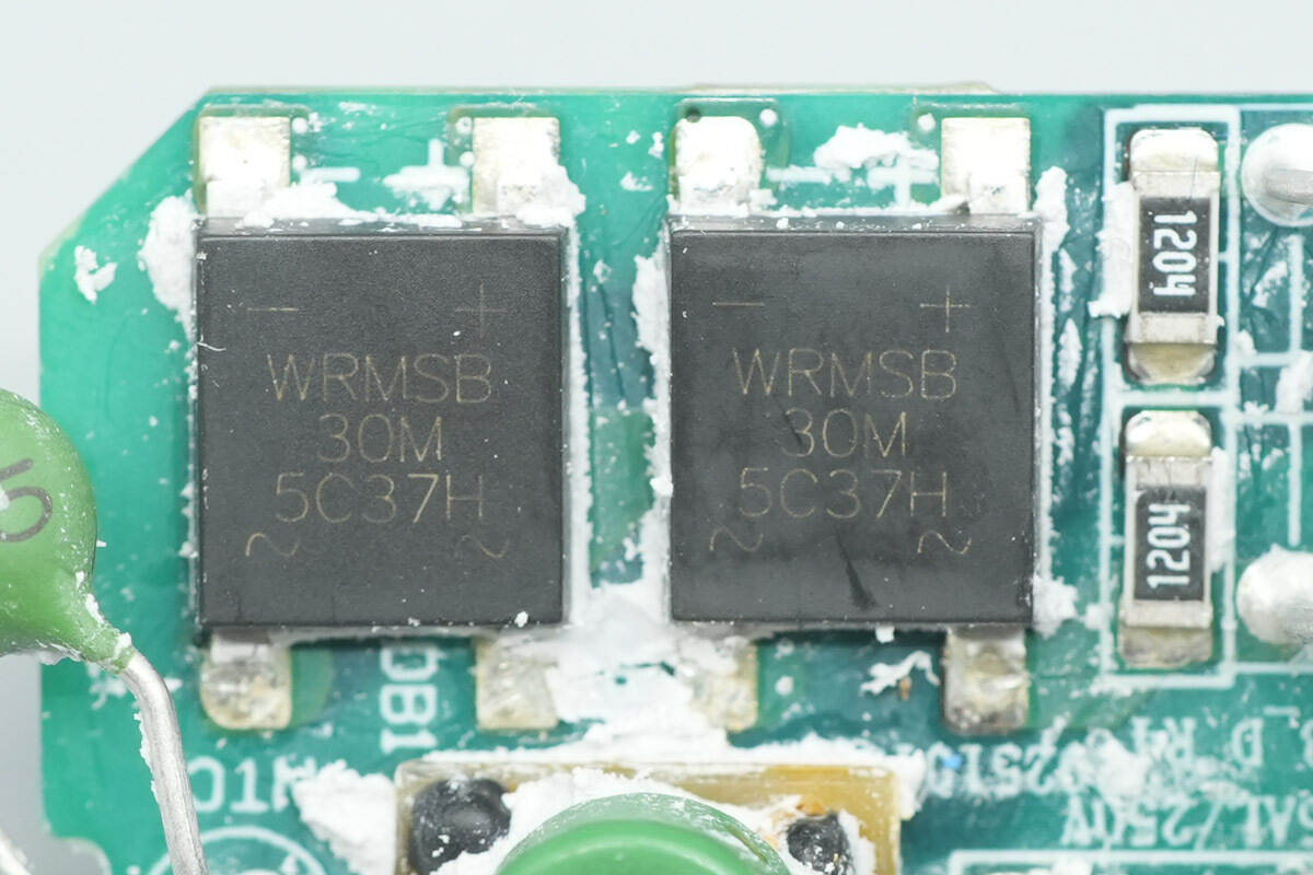
The bridge rectifiers are from World Industrial, model WRMSB30M, rated at 3 A 1000 V. This soft-recovery bridge features a gentle turn-off characteristic, which helps reduce diode junction capacitance and minimizes harmonic oscillations.
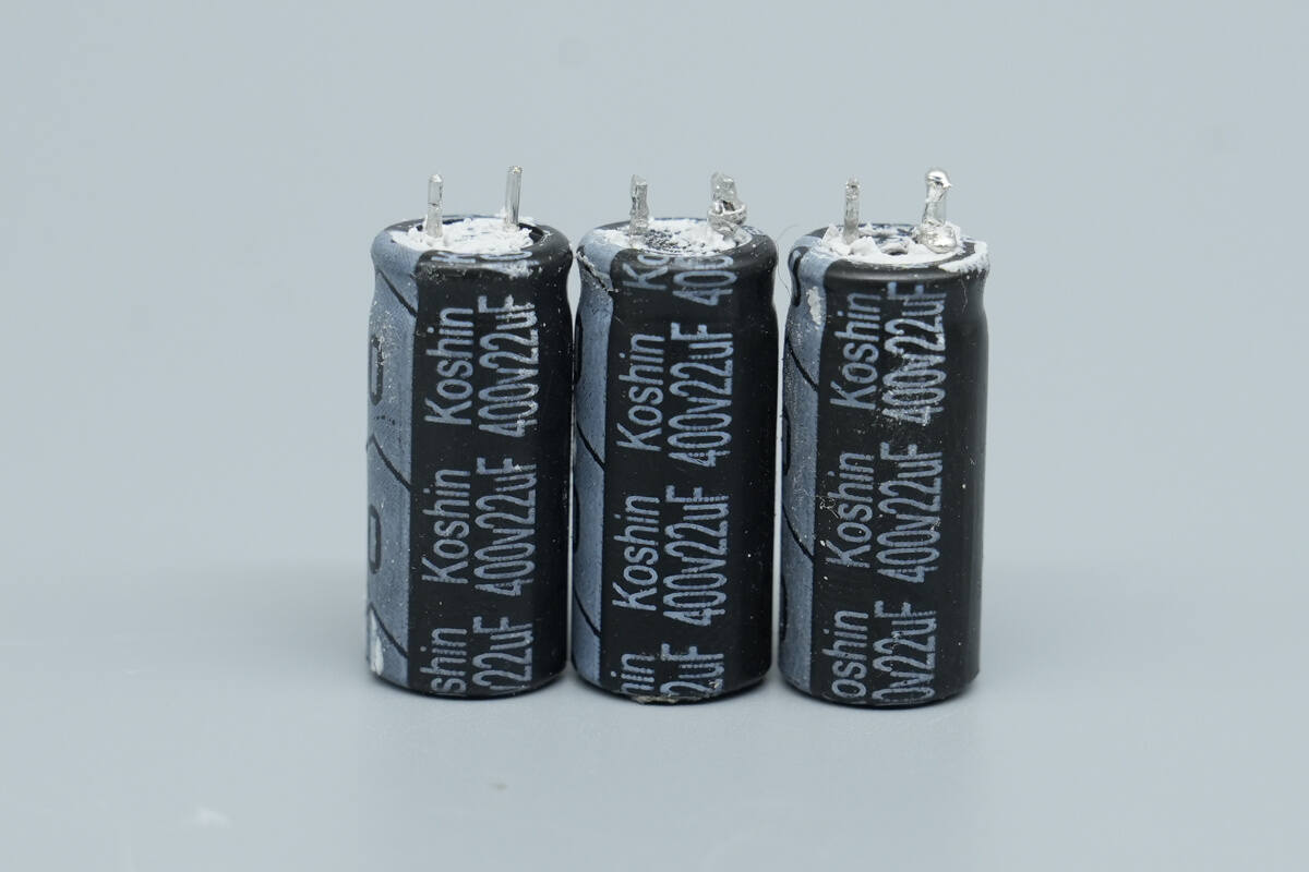
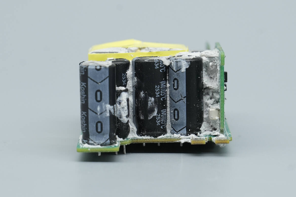
The five high-voltage filter electrolytic capacitors are all from Koshin, with three of them rated at 400 V, 22 μF.
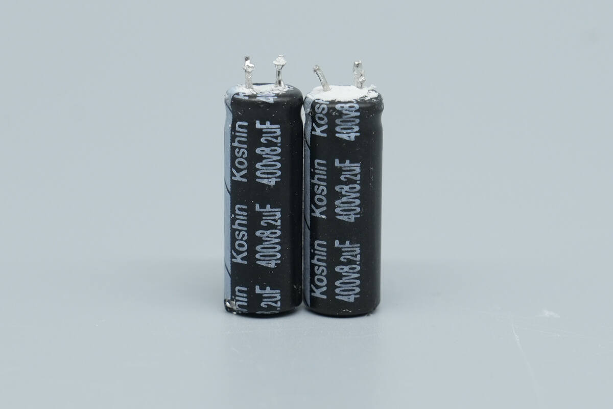
The other two capacitors are rated at 400 V, 8.2 μF.

The I-shaped inductor is insulated with heat-shrink tubing.

This side features a transformer, a synchronous rectifier controller, a synchronous rectifier, and an output filter solid capacitor.
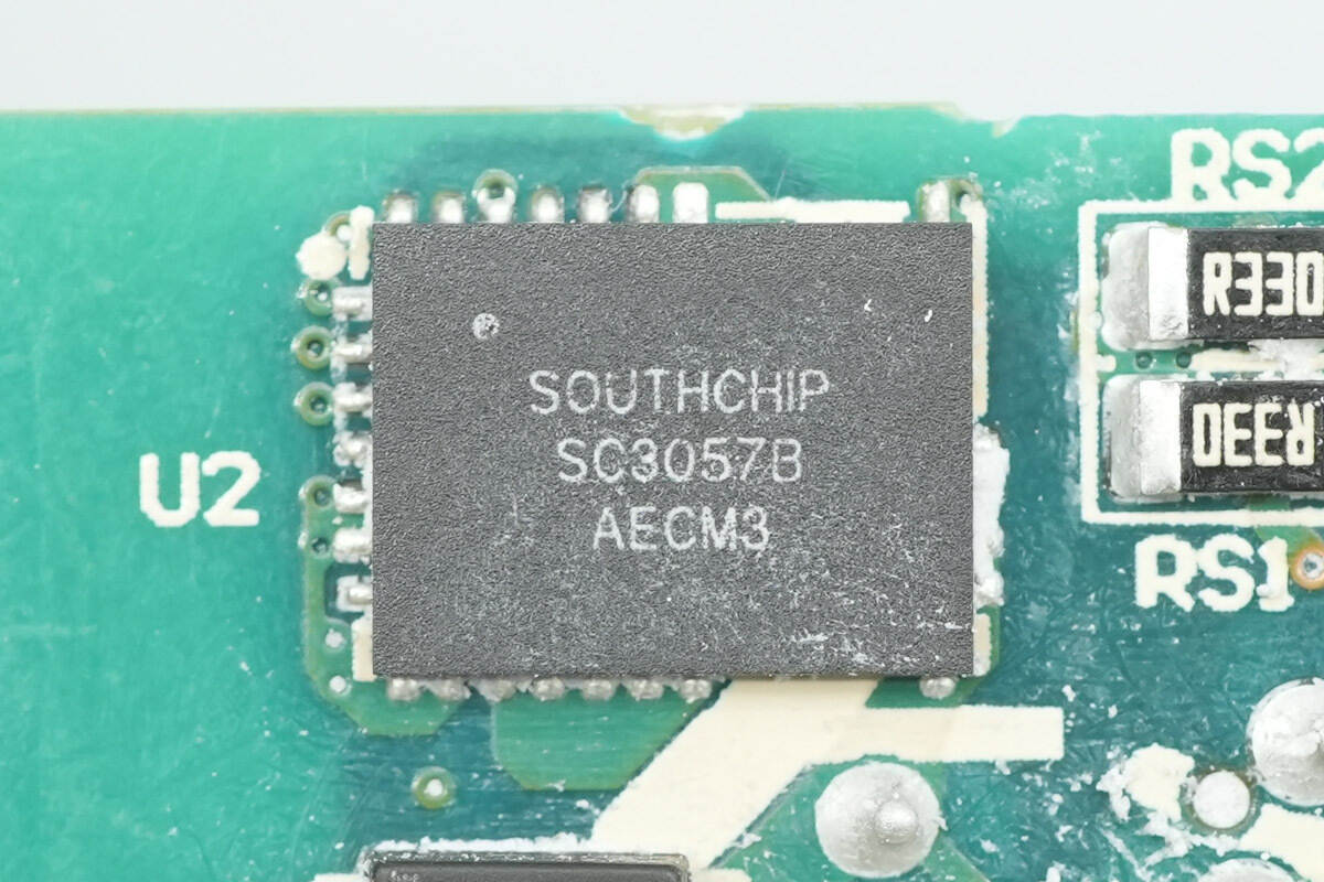
The master control chip is from SouthChip, model SC3057B. It is a high-frequency quasi-resonant flyback PWM converter featuring 700V GaN integration (QR/DCM), enabling high efficiency and reliability. The converter has a built-in X-capacitor discharge function and a high-voltage startup circuit via the HV pin. As a result, the HV pin allows for extremely low standby power consumption and ultra-fast startup time.
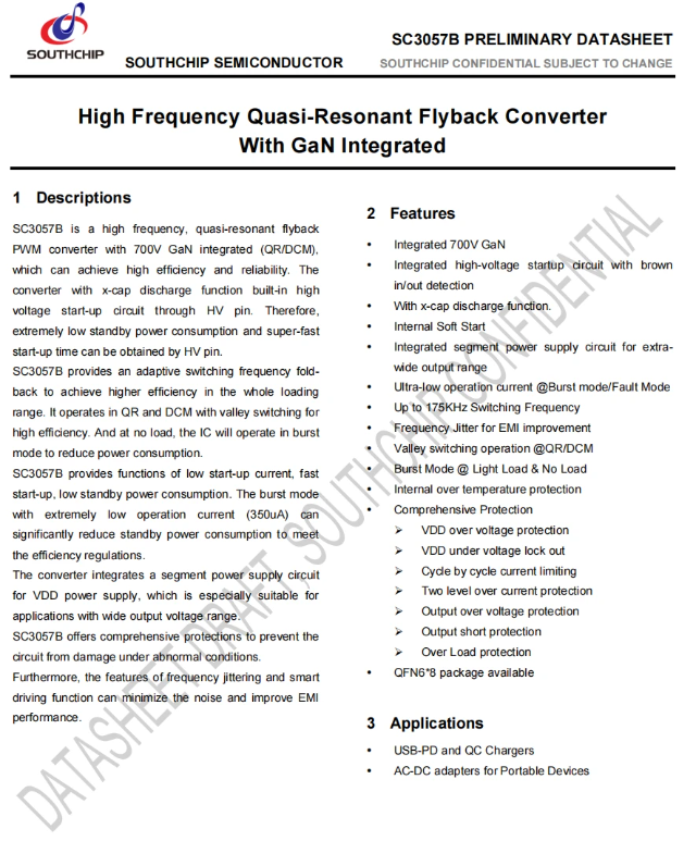
The SC3057B features adaptive switching frequency foldback to achieve higher efficiency across the full load range. It operates in valley-switching mode in both QR and DCM modes to enhance efficiency. Under no-load conditions, the IC switches to pulse mode to reduce power consumption.
The SC3057B offers low startup current, fast startup, and low standby power. Its extremely low operating current (350 µA) in pulse mode significantly reduces standby power, helping to meet efficiency regulation requirements. The SC3057B provides comprehensive protection features to prevent circuit damage under abnormal conditions. Additionally, frequency jitter and intelligent driving functions minimize noise and improve EMI performance. The SC3057B is available in a QFN 6×8 package.
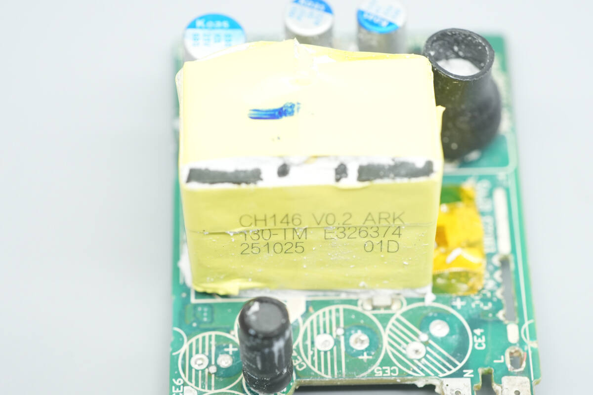
Close-up of the transformer.
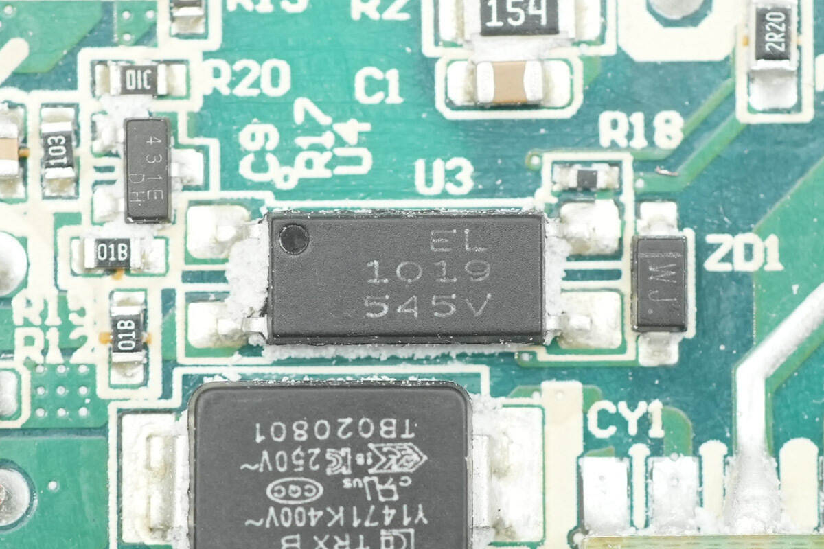
The Everlight EL1019 optocoupler is used for output voltage feedback.
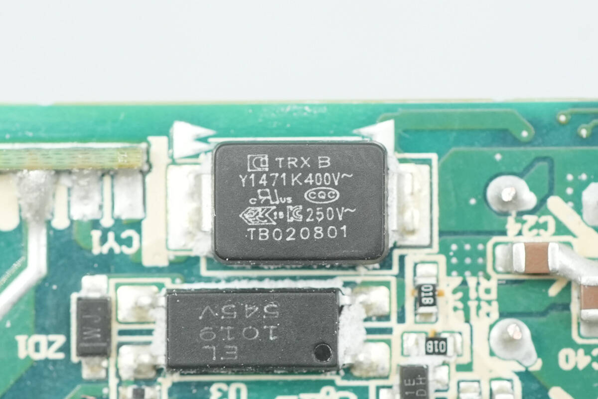
The SMD Y capacitor is from TRX. Its compact size and light weight make it ideal for high-density power products, such as GaN fast chargers. The part number is TMY1471K.
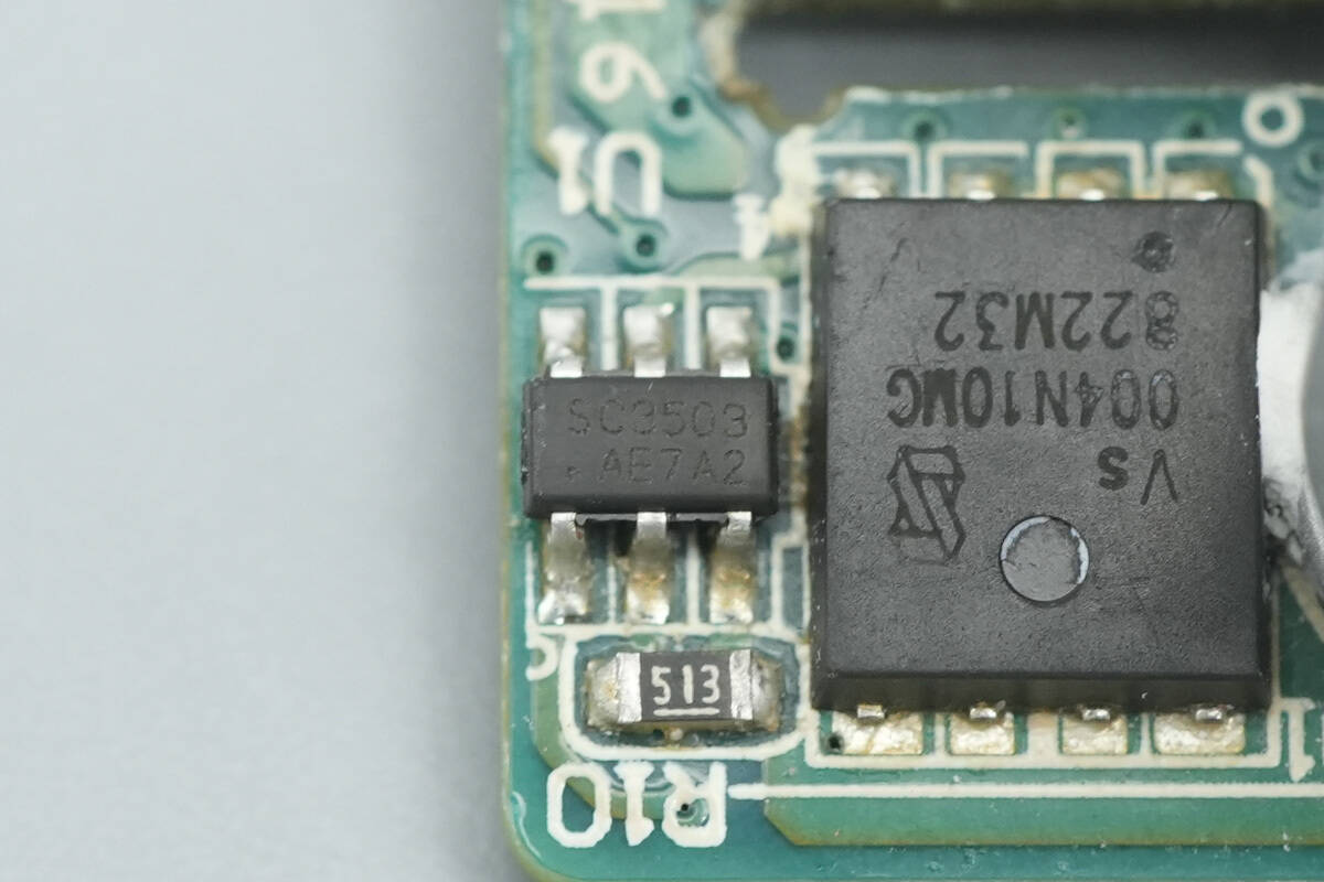
The synchronous rectifier controller is from SouthChip, model SC3503. It features adaptive turn-on detection and fast turn-off, requiring no auxiliary winding for power. The output voltage can go as low as 0 V. Its patented adaptive turn-on detection circuit prevents false conduction of the synchronous rectifier. The controller is compatible with a wide range of MOSFETs, has ultra-low quiescent current, supports multiple operating modes, and allows both high-side and low-side synchronous rectification. The external component count is minimal.
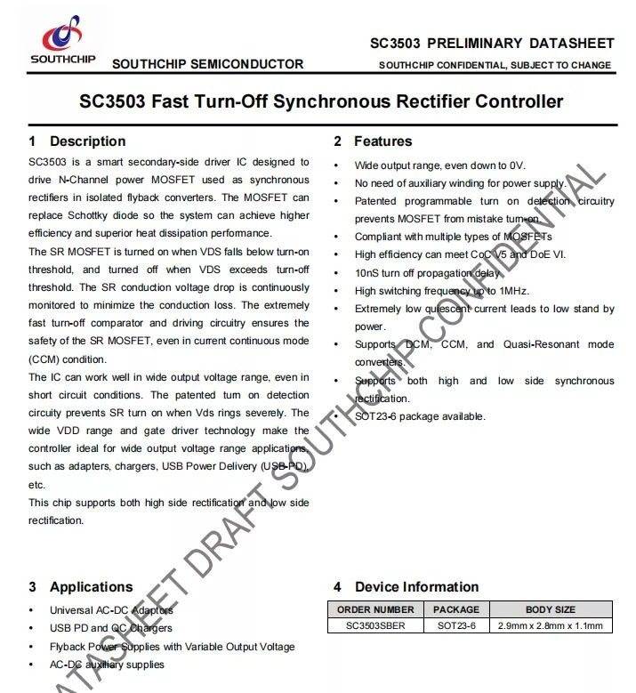
Here is the information about SouthChip SC3503.
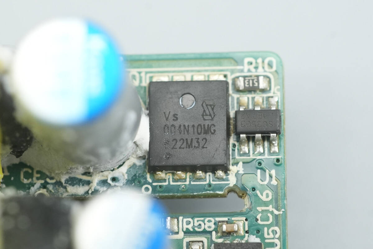
The synchronous rectifier is from Vergiga, model VSP004N10MS-G. It has a voltage rating of 100 V and an on-resistance of 3.8 mΩ, and comes in a PDFN 5×6×0 package.
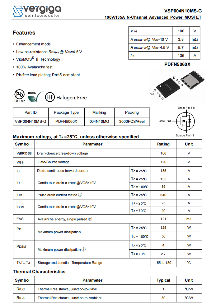
Here is the information Vergiga VSP004N10MS-G.
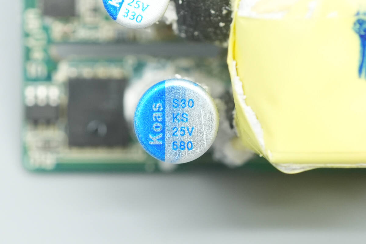
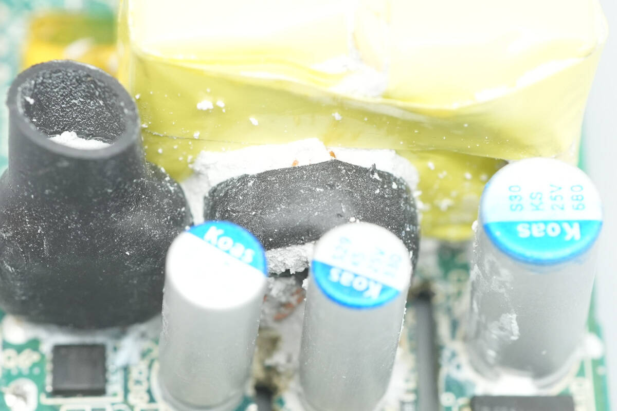
The solid capacitor for output filtering is also from Koshin, with a rating of 25 V, 680 μF.
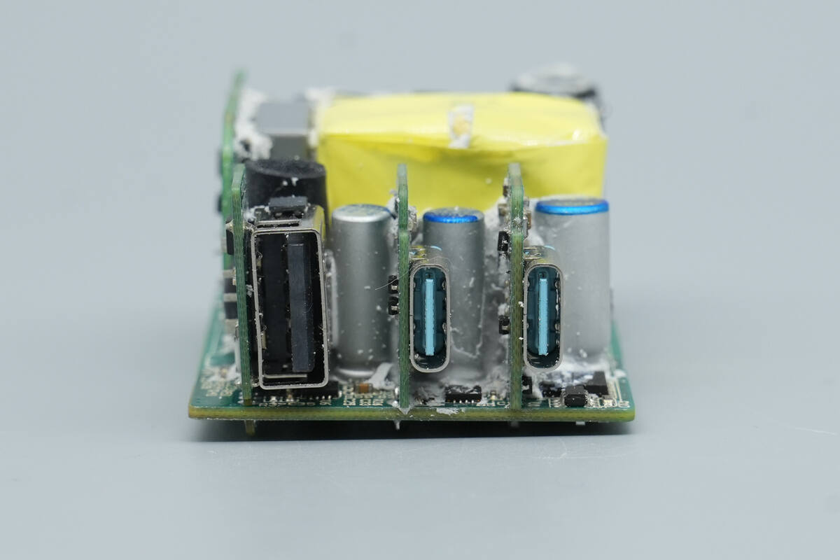
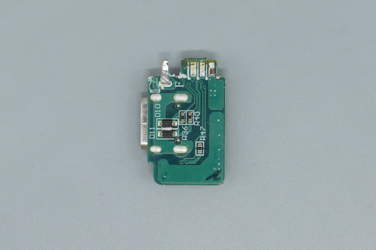
All three sockets are soldered onto separate PCBs.
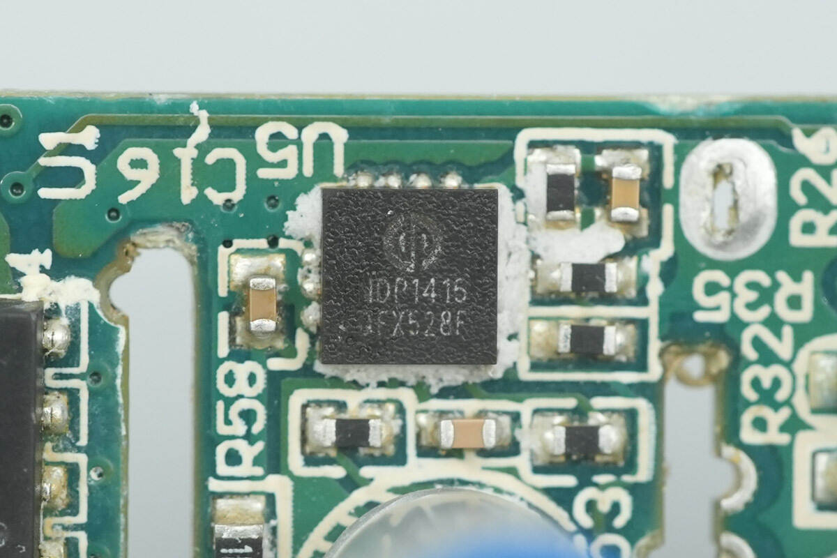
Both channels of the secondary step-down circuits use the NDP NDP1415 synchronous buck converter. The NDP1415 is a 40 V–rated synchronous buck converter that supports input voltages up to 38 V. It features constant-voltage and constant-current regulation, integrated line-loss compensation, adjustable output voltage and switching frequency, burst mode operation, built-in loop compensation, and soft-start functionality. The device is packaged in a QFN-16 form factor.
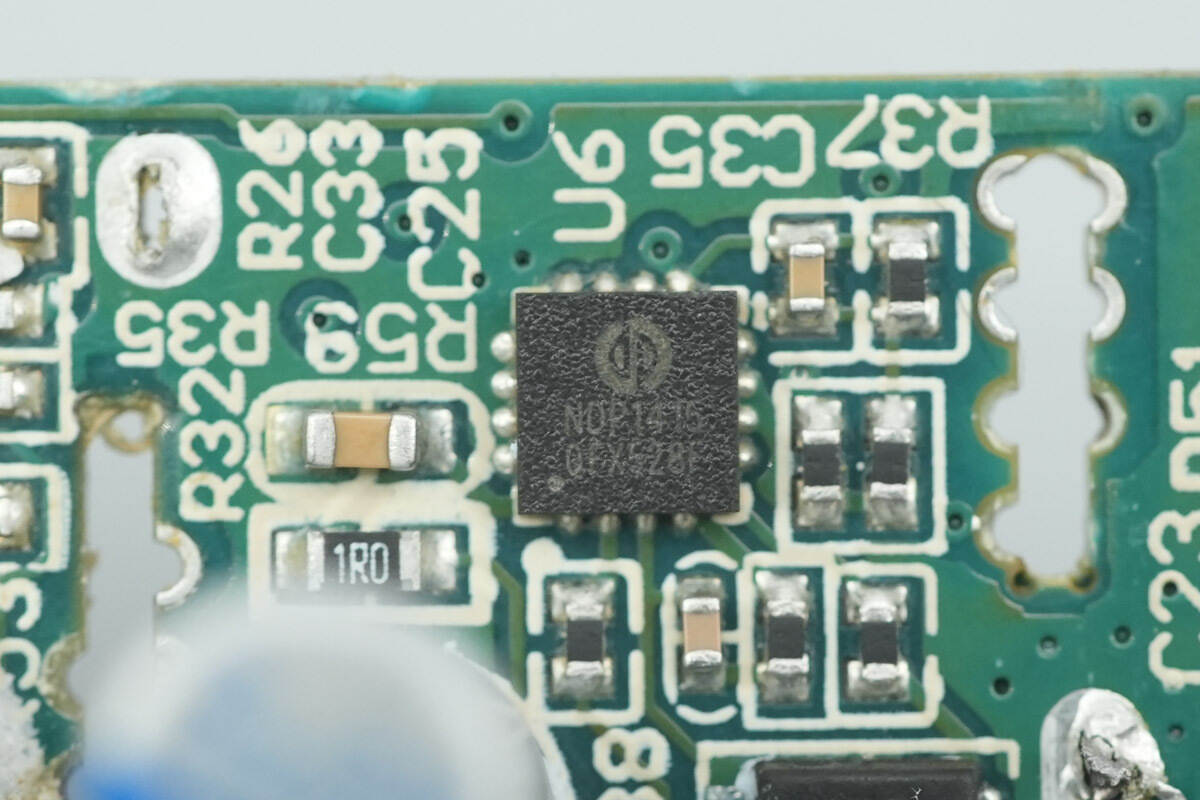
Close-up view of another NDP NDP1415 synchronous buck converter.
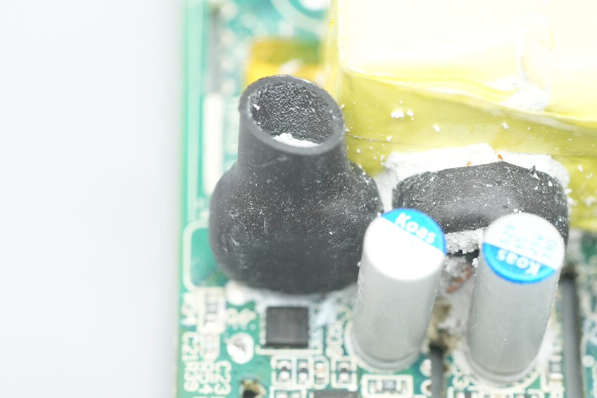
The matching step-down inductor is insulated with heat-shrink tubing.
Another step-down inductor is located nearby.
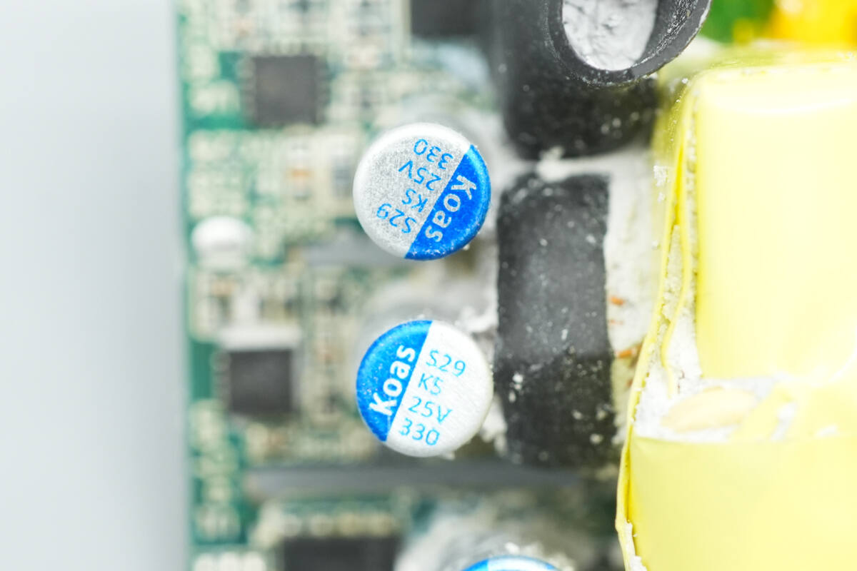
The two secondary filter solid-state capacitors are also sourced from Koshin, each rated at 25 V and 330 µF.
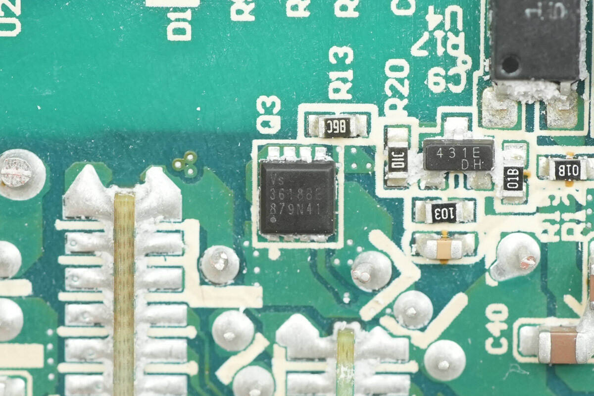
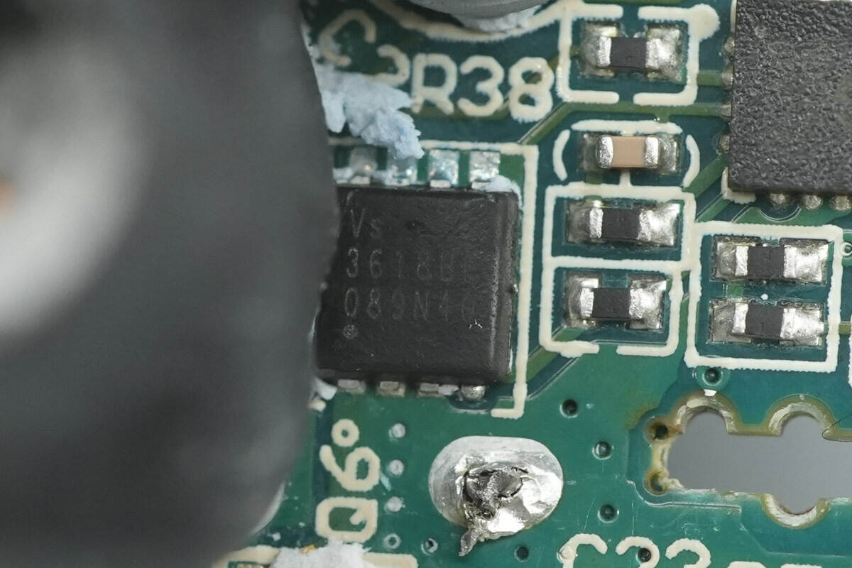
The VBUS MOSFET is from Vergiga, model VS3618BE. It is an N-channel MOSFET rated at 30 V with an on-resistance of 5.2 mΩ, packaged in a PDFN3333 form factor.
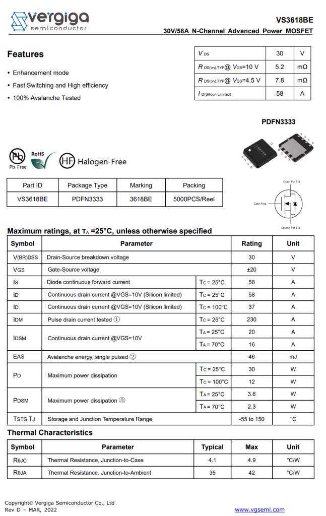
Here is the information about Vergiga VS3618BE.
A Vergiga VS3618BE VBUS MOSFET is also placed on the front side.
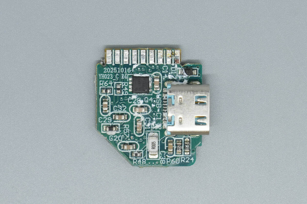
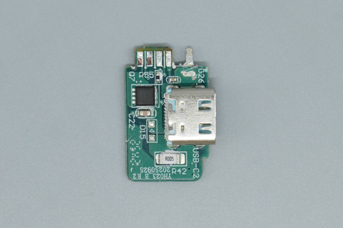
The small PCB of the USB-C1 socket has an output VBUS MOSFET mounted on its front side.
The opposite side is populated with the protocol chip.
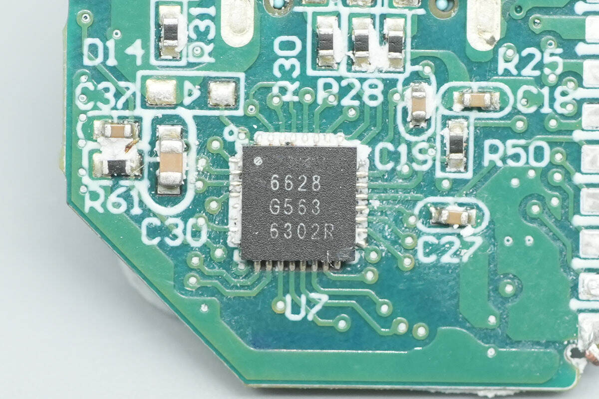
The protocol chip is from JADARD, model JD6628. This device is certified for PD 3.1 EPR with TID 10463 and supports the 28 V EPR output level. It integrates UFCS, Huawei SCP/FCP, and Qualcomm QC5 protocols, and also supports proprietary fast-charging protocols, meeting the requirements of mainstream products.

The JADARD JD6628 supports dual independent fast-charging channels and is compatible with all fast-charging protocols. It features multi-interface control and constant-voltage/constant-current regulation. The chip provides comprehensive protection, including output overvoltage, undervoltage, and overcurrent protection, input overvoltage and undervoltage protection, as well as D+/D– and CC pin overvoltage protection. It also includes line-loss compensation and is available in TQFN-32L and TQFN-40L packages.
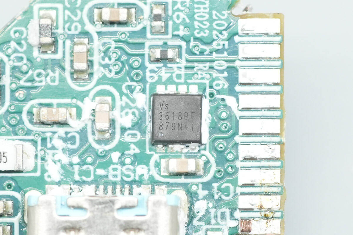
The output VBUS MOSFET for the USB-C1 port also uses the Vergiga VS3618BE.
The front side of the small PCB for the USB-C2 socket is equipped with a VBUS MOSFET.
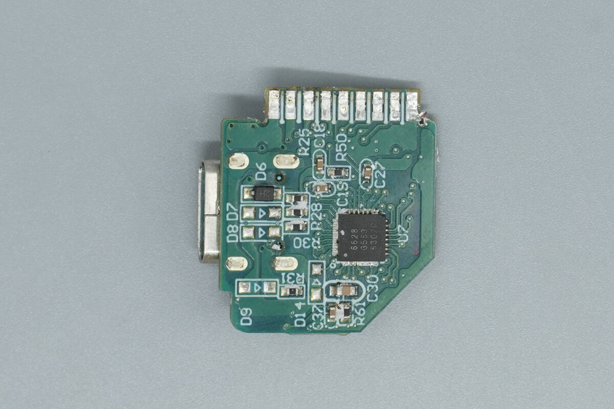
Overview of the opposite side of the small PCB.
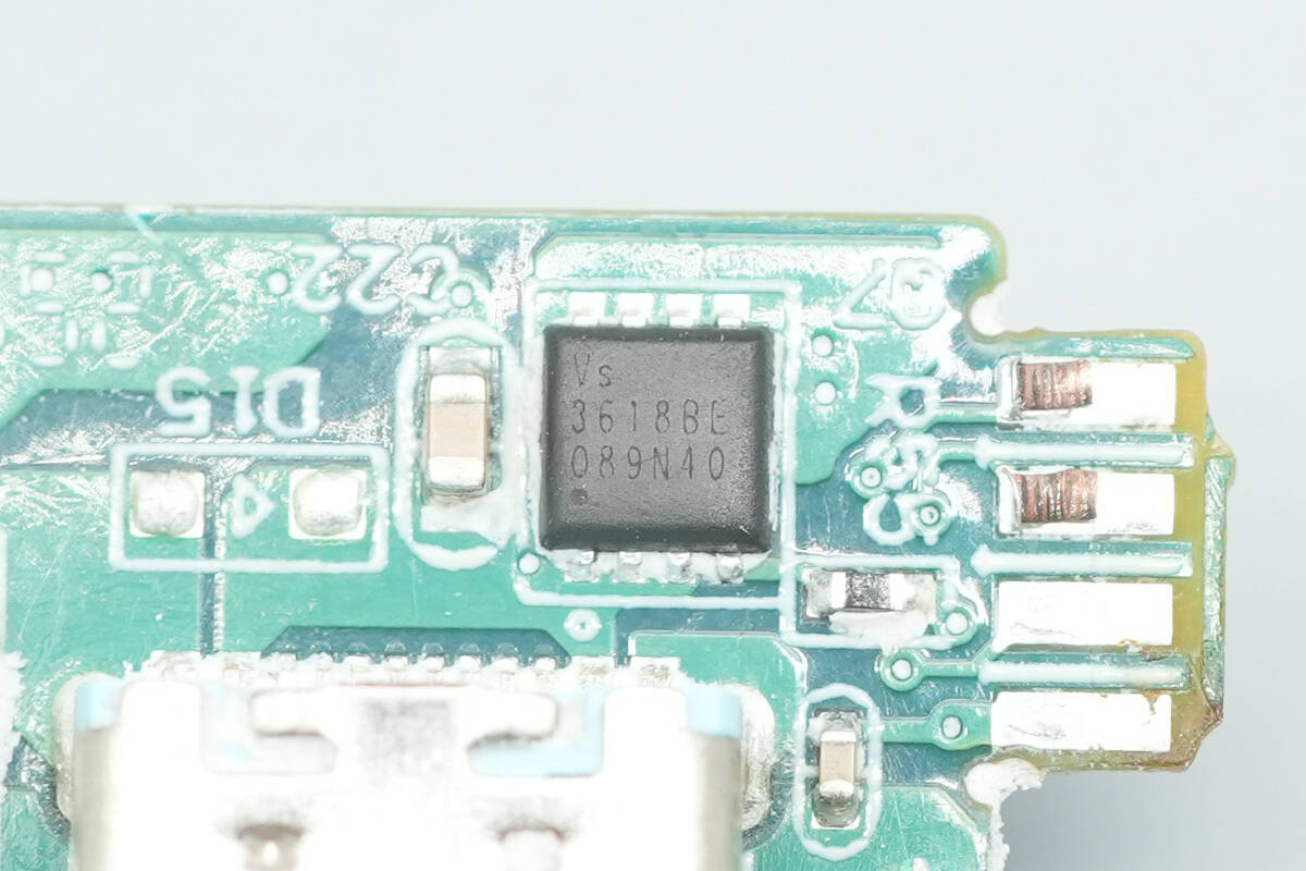
The output VBUS MOSFET for the USB-C2 port also uses the Vergiga VS3618BE.
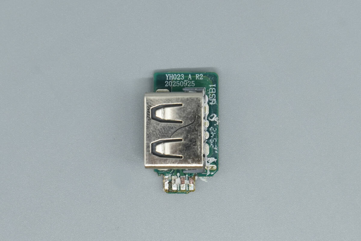
Front-side overview of the small PCB for the USB-A socket.
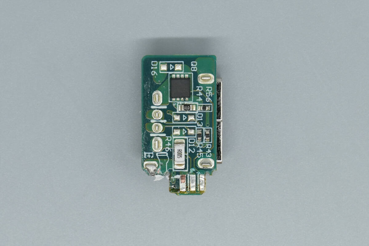
The opposite side is equipped with an output VBUS MOSFET.
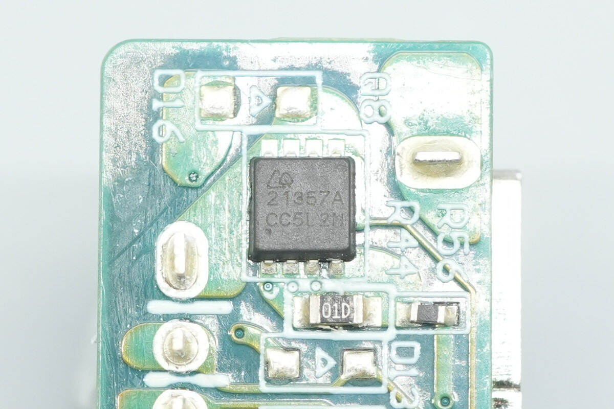
The output VBUS MOSFET for the USB-A port is from CQAOS, model CQY21357A. It is a P-channel MOSFET rated at –30 V with an on-resistance of 11 mΩ, packaged in a DFN3x3EP form factor.
Well, those are all components of the HONOR SuperCharge 66W Power Adapter.
Summary of ChargerLAB
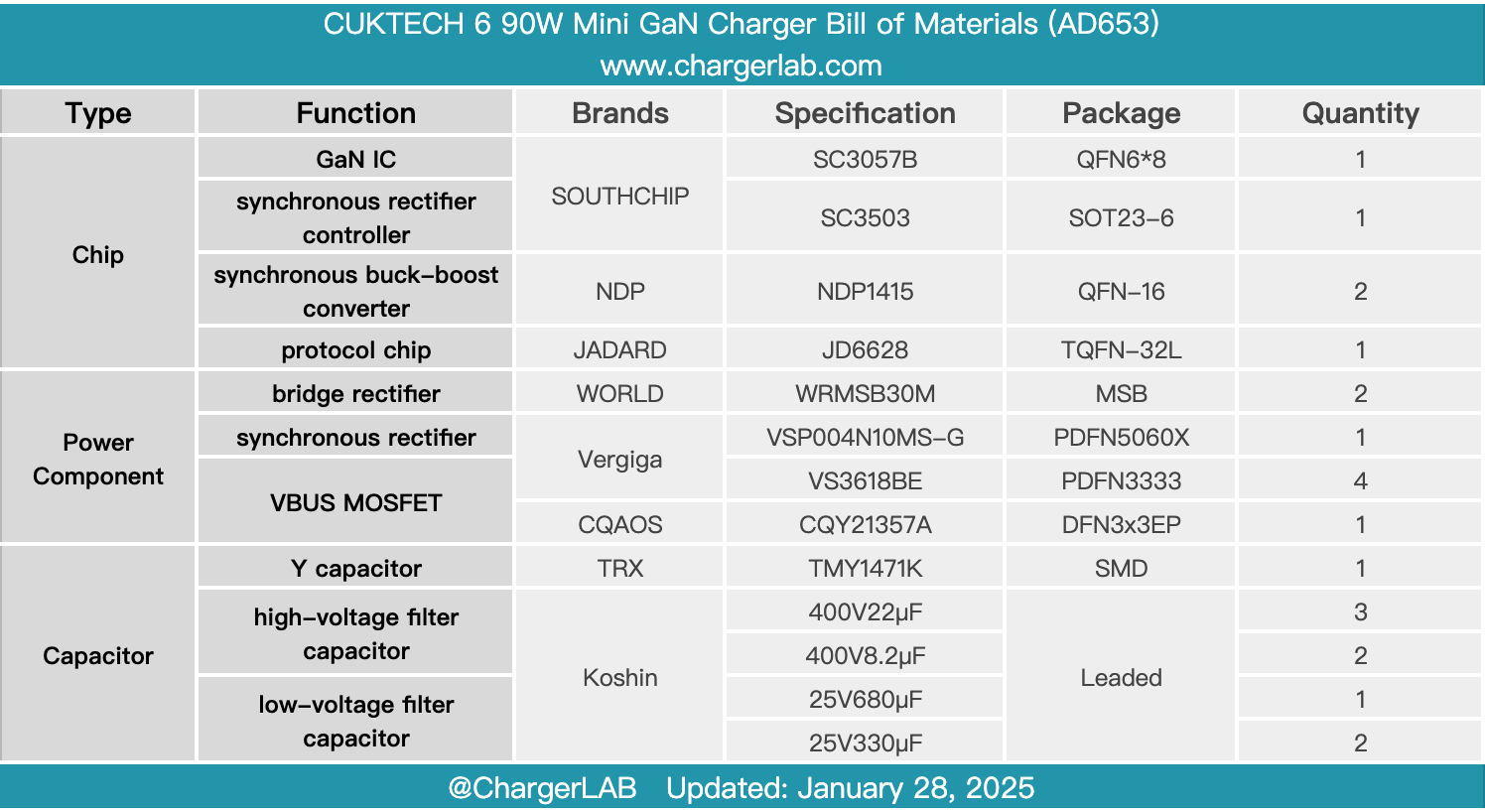
Here is the component list of the HONOR SuperCharge 66W Power Adapter for your convenience.
After taking it apart, we found that it adopts a highly integrated design to minimize size. On the primary side, a SouthChip SC3057B high-frequency QR GaN IC serves as the power core, paired with an SC3503 synchronous rectifier controller and Vergiga synchronous rectifiers, forming a high-efficiency, compact flyback architecture.
On the secondary step-down side, both DC-DC buck circuits use the NDP NDP1415 solution, controlled by the JADARD JD6628 protocol chip to ensure stable delivery of 90 W high-power rapid charging and 65 W PD fast charging. The PCBA modules are encapsulated with potting, enhancing structural integrity and thermal performance, resulting in a solid and reliable build quality.
Related Articles:
1. Teardown of Xiaomi 140W 8-in-1 Desktop Charging Station (XMCDZ-03QM)
2. Teardown of HONOR SuperCharge 66W Power Adapter (HN-110600CP0)
3. Teardown of Lenovo Thinkplus FLUXO 125W 12800mAh Portable Power Bank (PBFO-12125A)