Introduction
CUKTECH recently launched the 10 GaN Charger Ultra. Compared to the previous CUKTECH 30 Charging Station Ultra, this model is designed with portability in mind to better suit travel needs. It comes with three USB-C ports and one USB-A port, supports 100W PD fast charging, and is compatible with UFCS, PPS, and SCP protocols. It also supports Xiaomi 120W proprietary protocol.
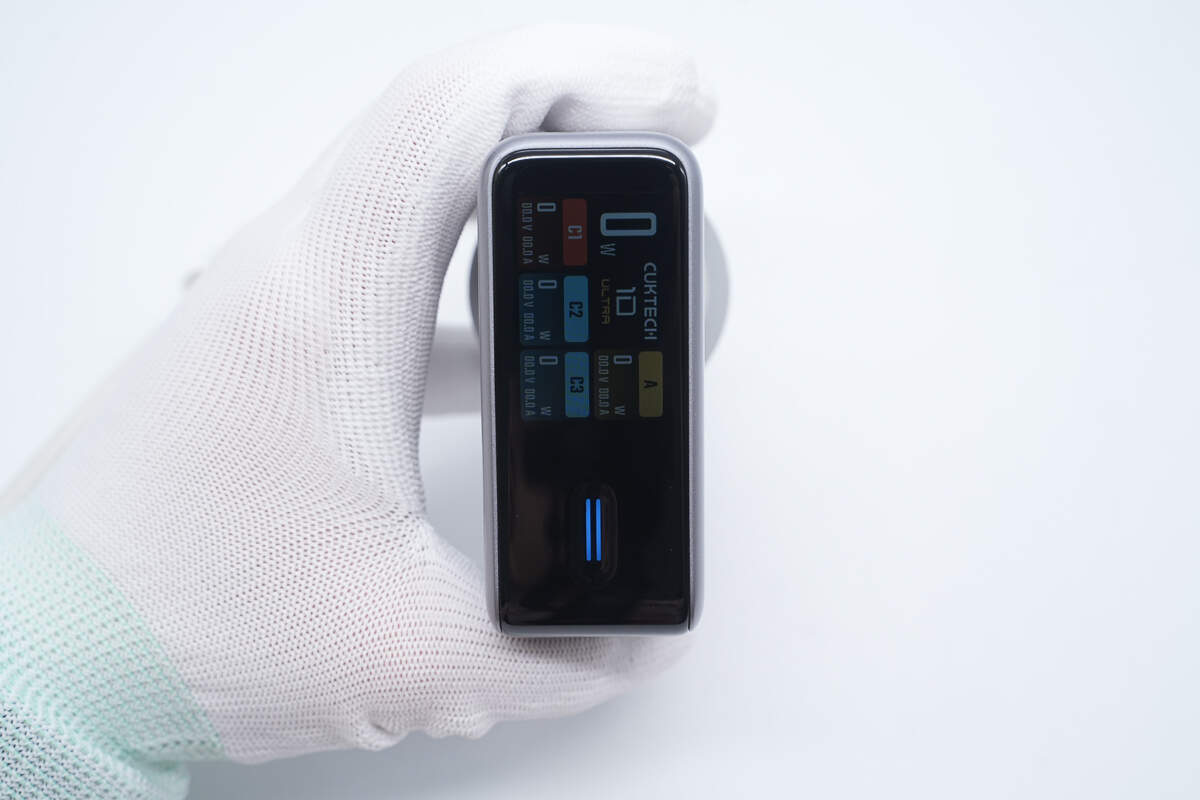
It features a 1.57-inch screen and supports Bluetooth connectivity with the Xiaomi Home. Users can view real-time data such as total output power, individual port power, current, voltage, charging curves, and temperature. It also supports OTA updates for continuous upgrades. Let’s take a look at the internal design and components.
Product Appearance
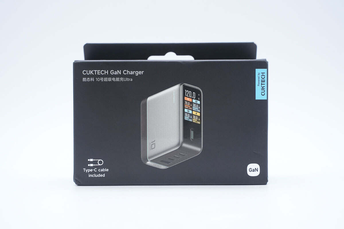
The front of the packaging features the product name, an image of the device, GaN, and Powered by CUKTECH.
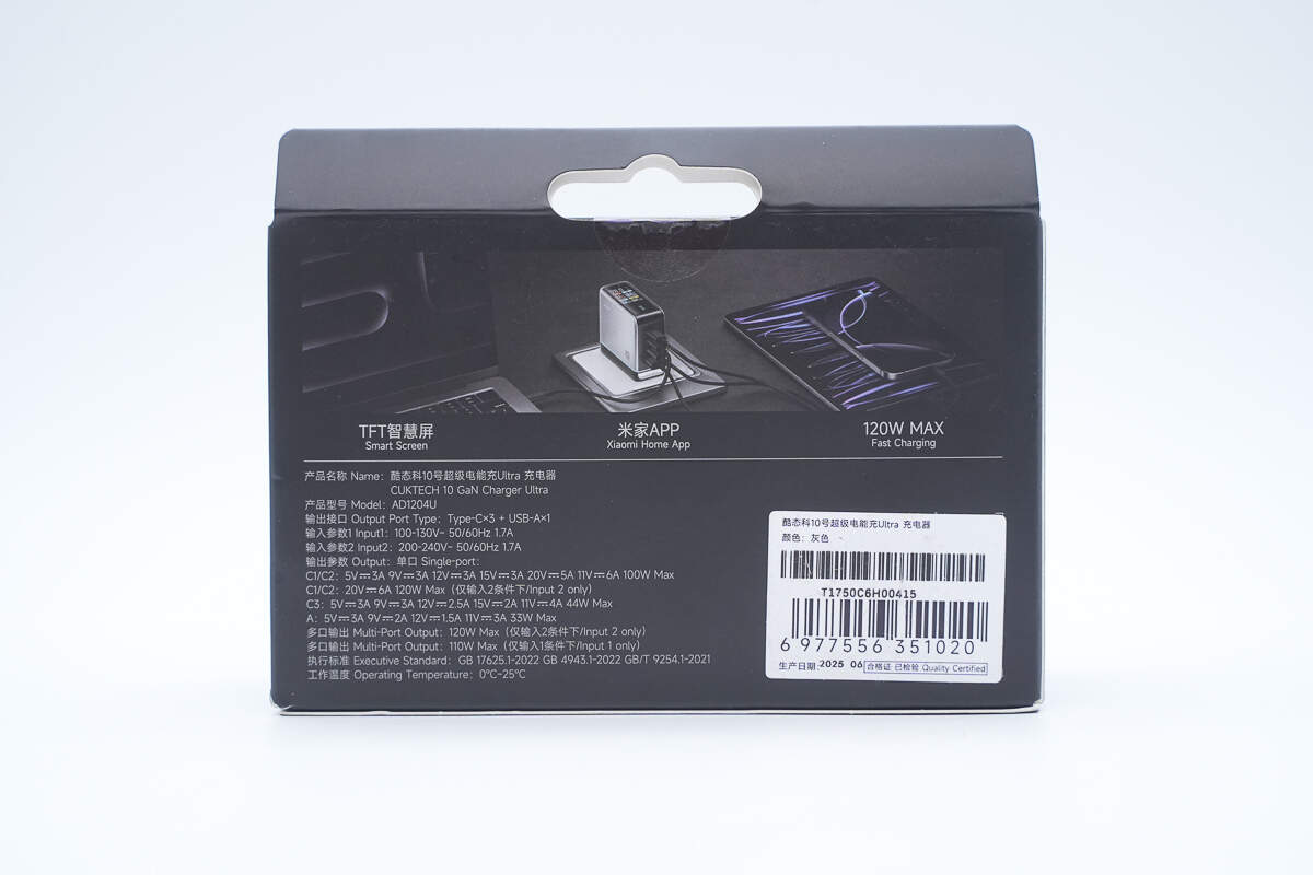
The back displays usage scenarios and the specification information.
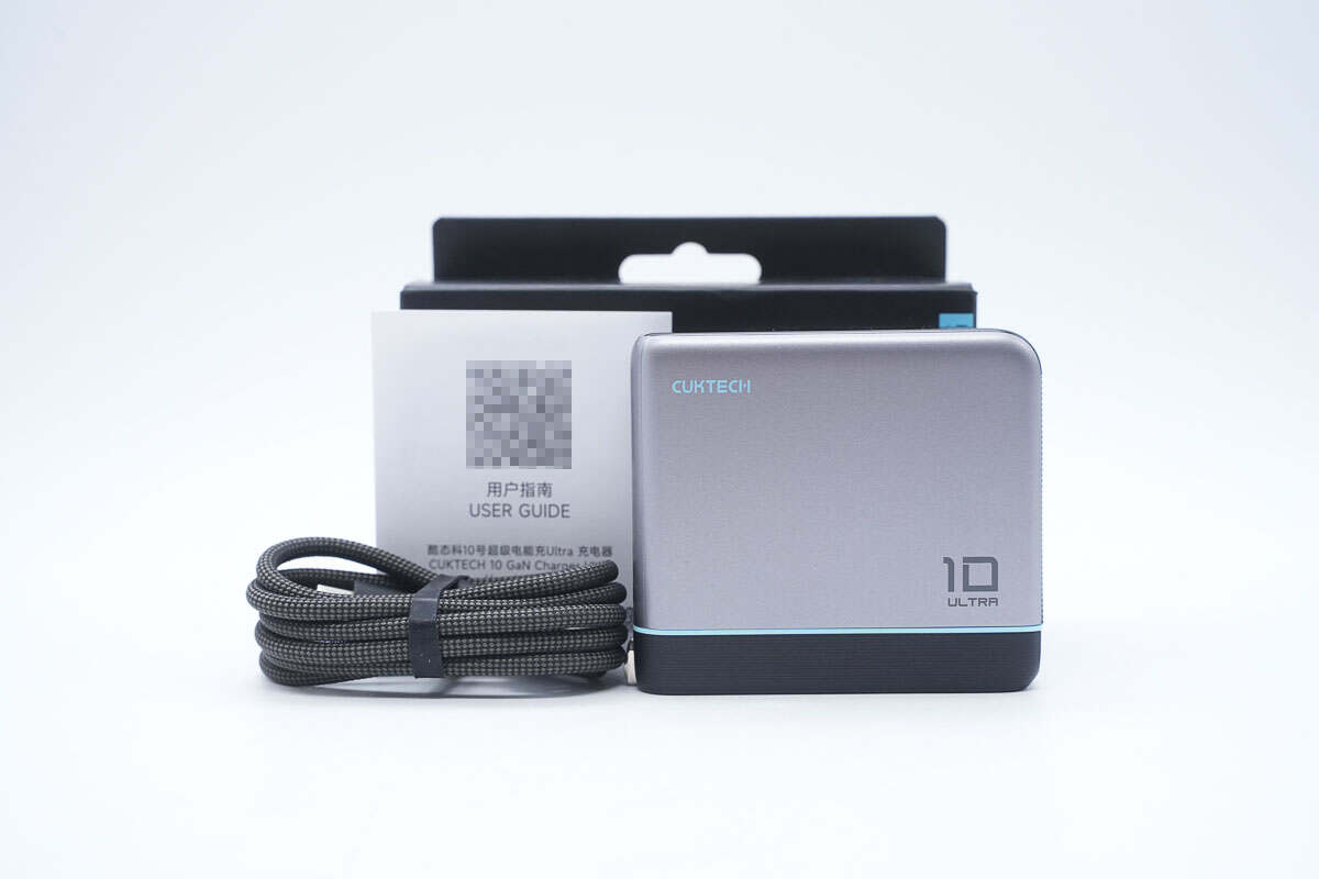
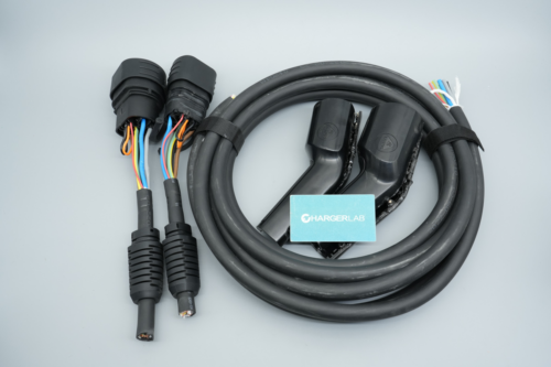
The package includes the charger, cable, and some documents.

The included USB-C cable supports up to 6A current.
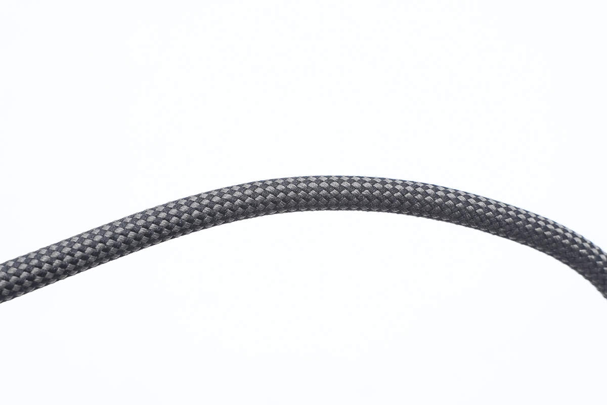
It uses a black and silver two-tone braided design, making it more resistant to dirt and more durable.
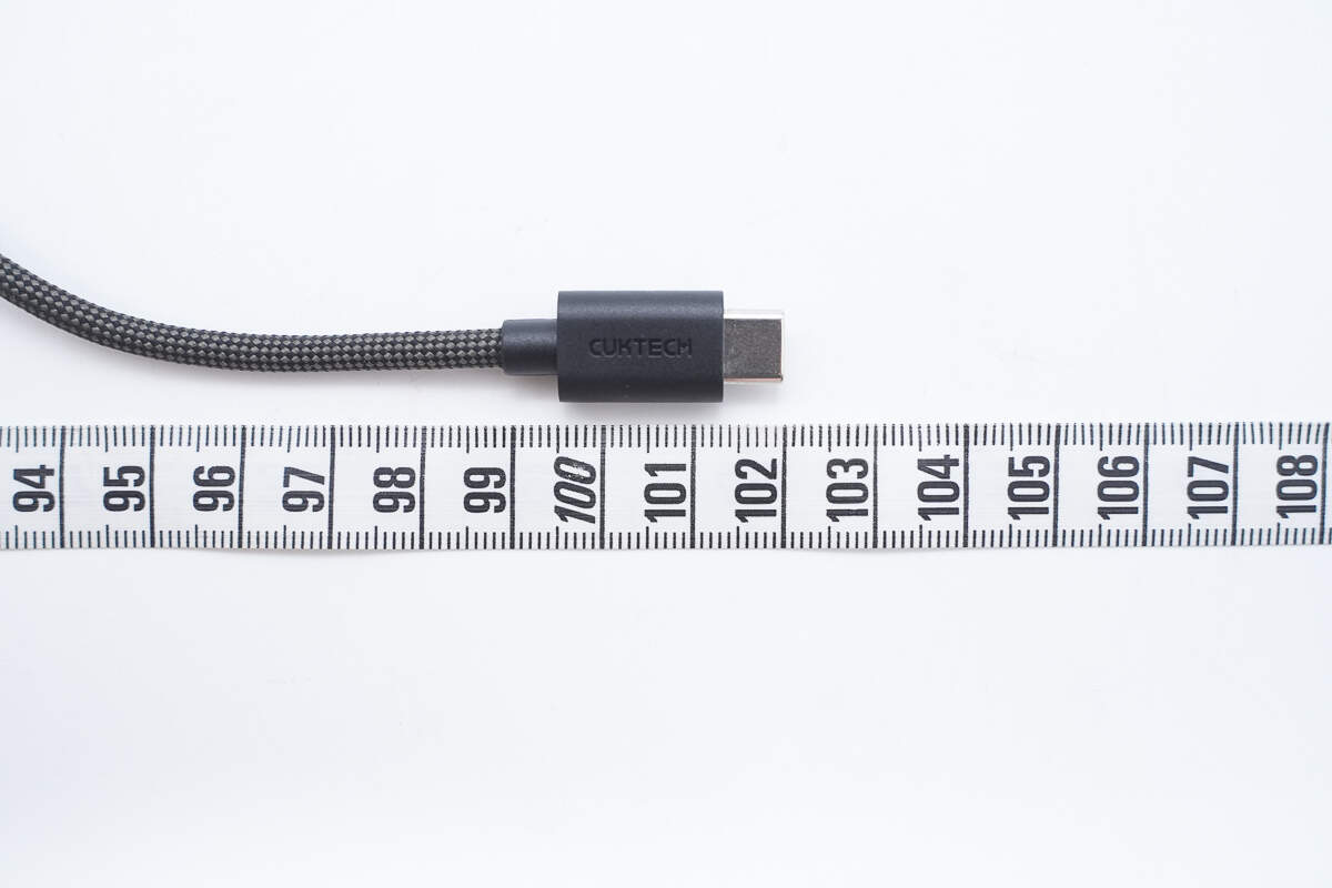
The length is about 1 m (3' 3.37'').
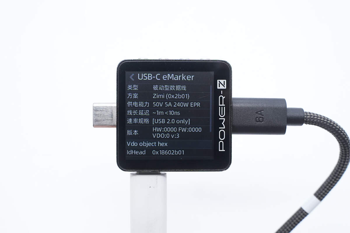
ChargerLAB POWER-Z KM003C shows it has an E-Marker chip, supports power delivery of 50V/5A, and offers data transfer capability at USB 2.0 speeds.
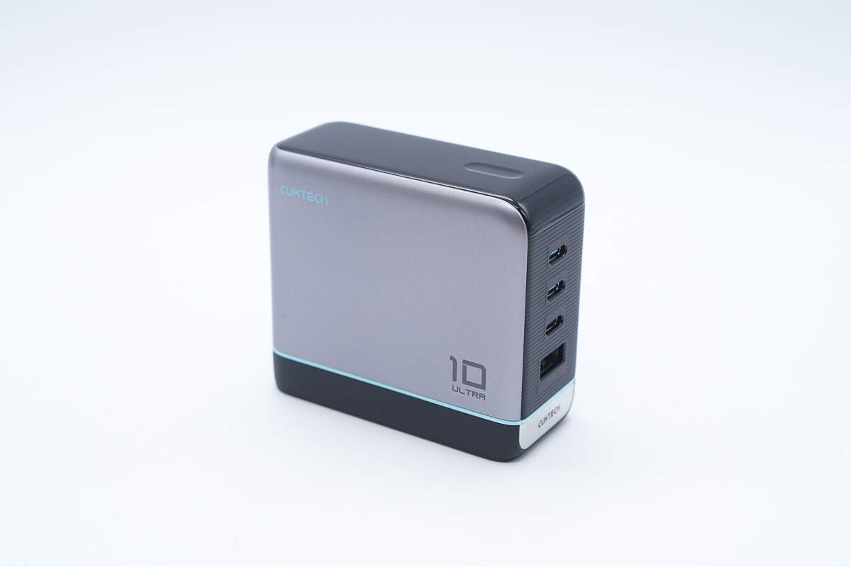
The charger features smoothly rounded corners, giving it a refined and premium feel.

The front is printed with the CUKTECH logo and the “10 ULTRA”.
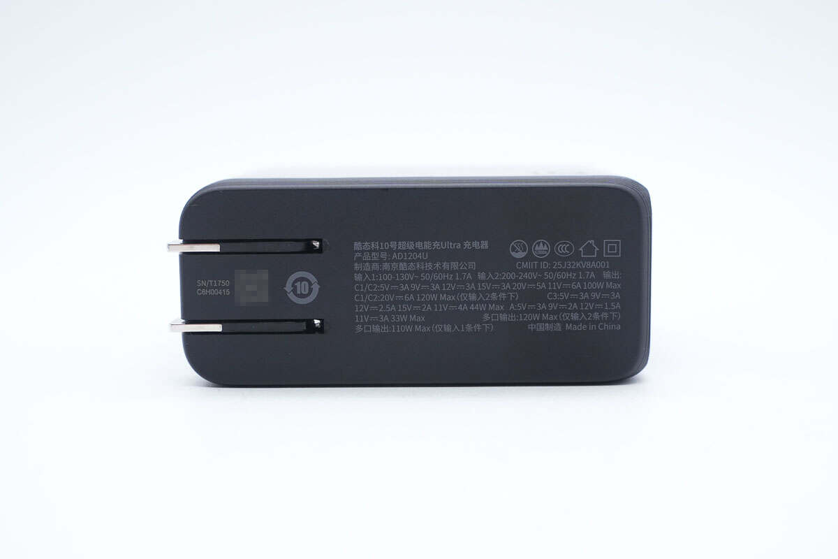
The specification information is also printed on the bottom.
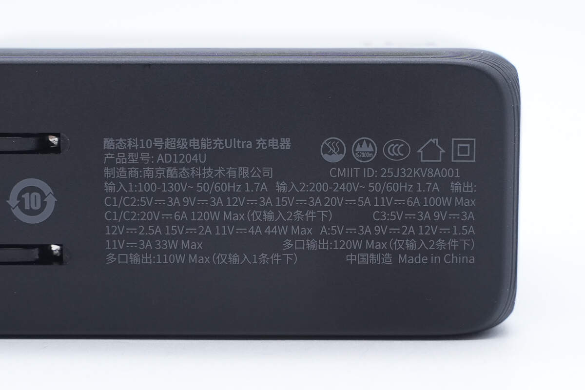
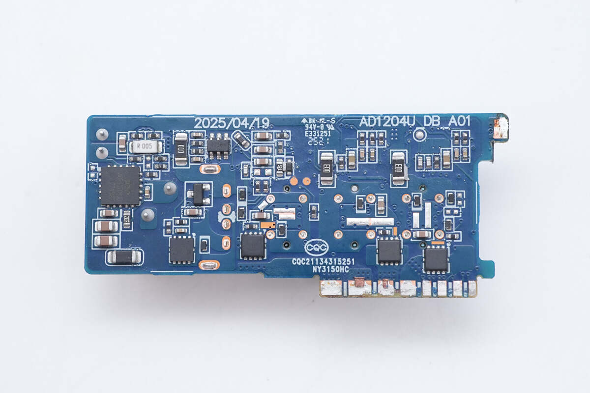
Model: AD1204U
Input 1: 100-130V\~ 50/60Hz 1.7A
Input 2: 200-240V\~ 50/60Hz 1.7A
Output:
USB-C1 and USB-C2 support 5V/3A, 9V/3A, 12V/3A, 15V/3A, 20V/5A, and 11V/6A with a maximum power of 100W.
Under Input 2 conditions only, USB-C1 and USB-C2 support 20V/6A with a maximum power of 120W.
USB-C3 supports 5V/3A, 9V/3A, 12V/2.5A, 15V/2A, and 11V/4A with a maximum power of 44W.
USB-A supports 5V/3A, 9V/2A, 12V/1.5A, and 11V/3A with a maximum power of 33W.
Multi-port output is up to 120W under Input 2 conditions and up to 110W under Input 1 conditions.
The charger is certified by CCC.
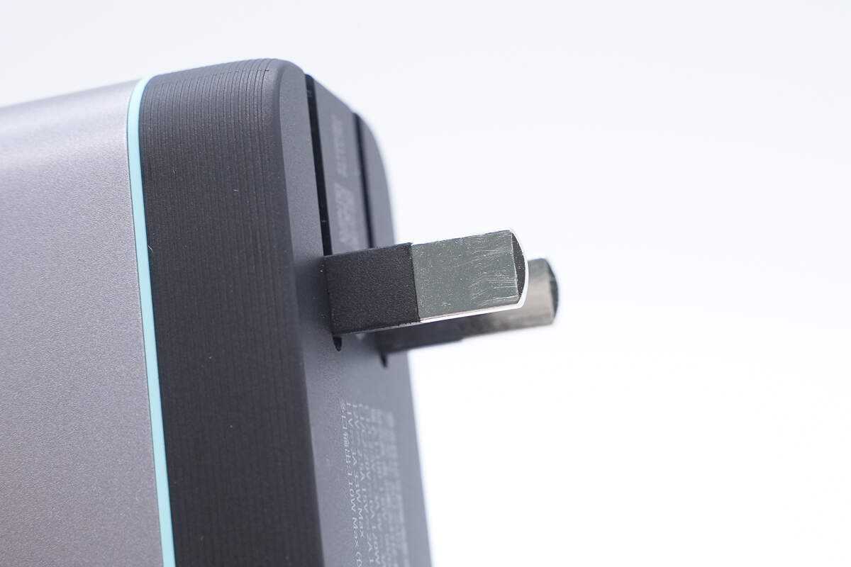
It features foldable prongs for easy portability.
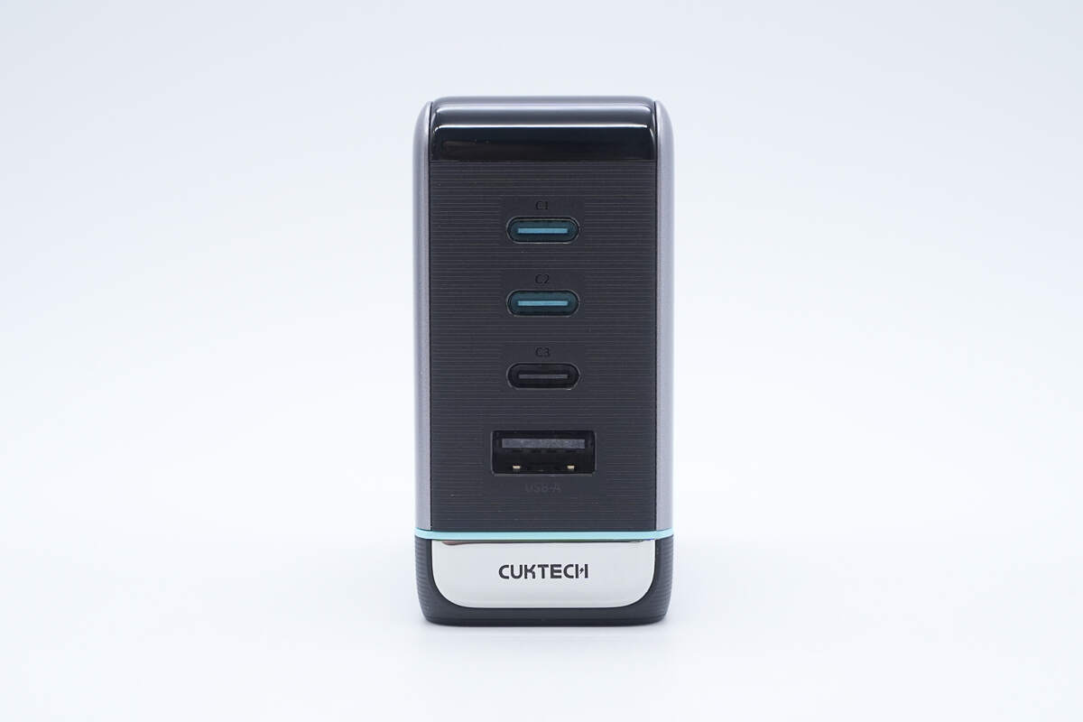
The name of each port is printed next to it, and the CUKTECH logo is laser-engraved below.
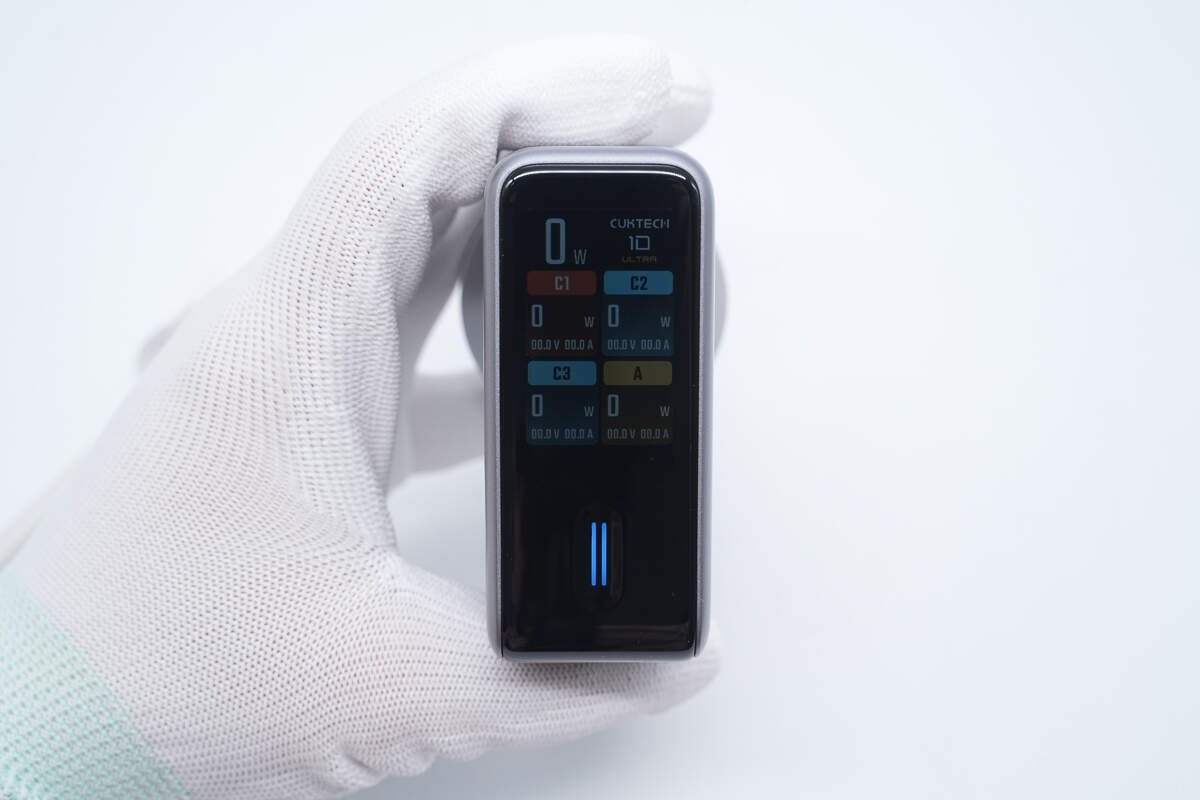
The 1.57-inch screen with a peak brightness of 700 nits and a 160° viewing angle. It can display total output power, temperature, and individual port power/current/voltage. The UI can be rotated 90°.
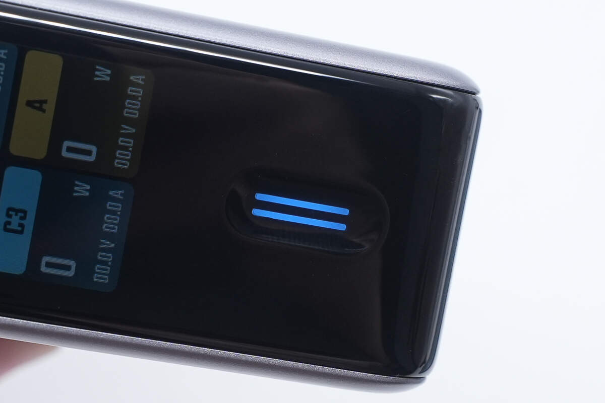
The touch button features a recessed design.
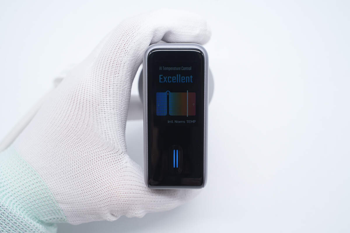
Tap the touch button can switch between function interfaces.
Press and hold to rotate the UI 90° for an optimal viewing angle.
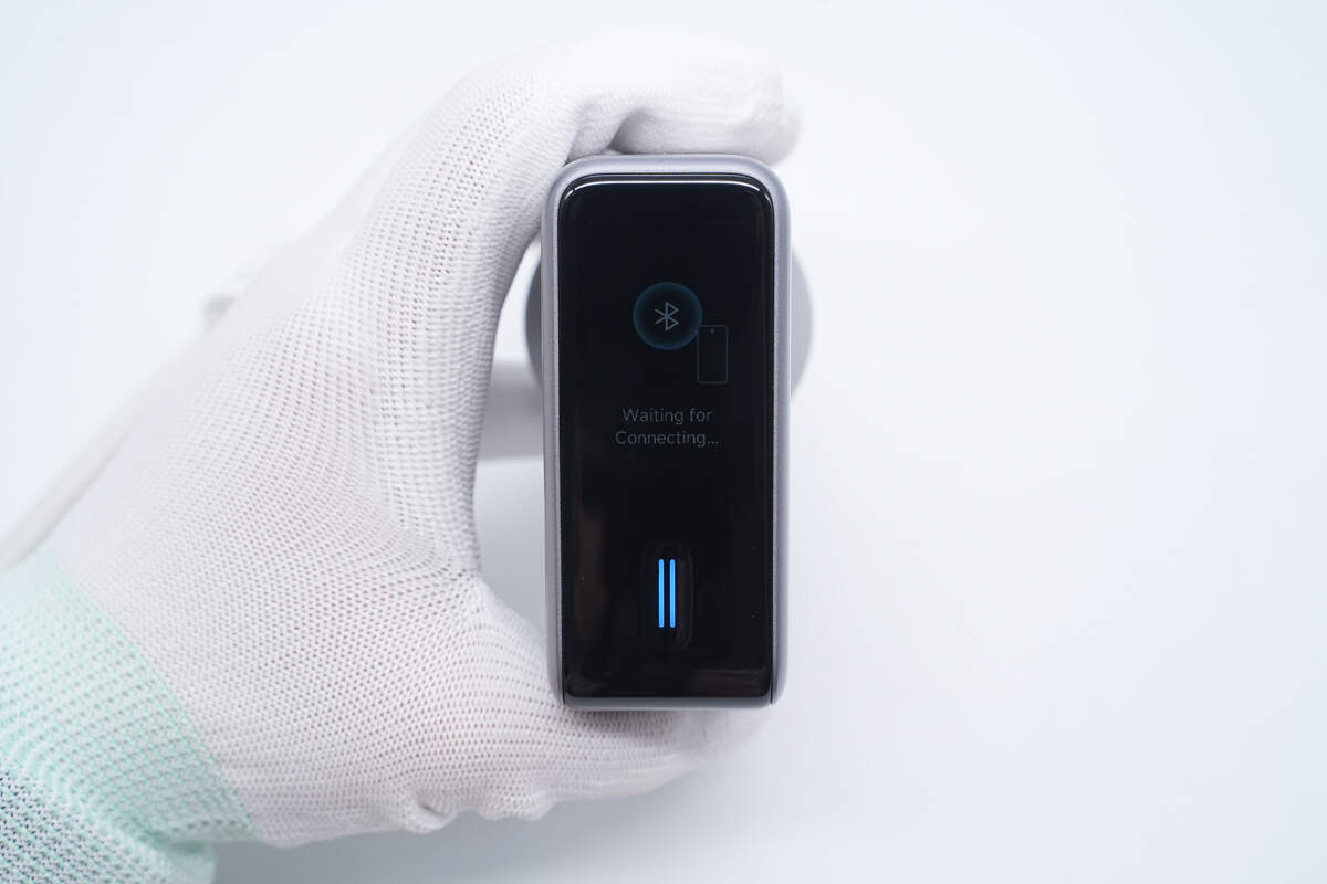
A major selling point is its ability to connect to Xiaomi Home via Bluetooth, enabling a wide range of customizable features and supporting OTA updates.
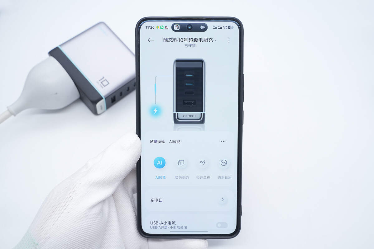
Through the Mi Home app, users can configure four output modes based on their usage habits and needs.
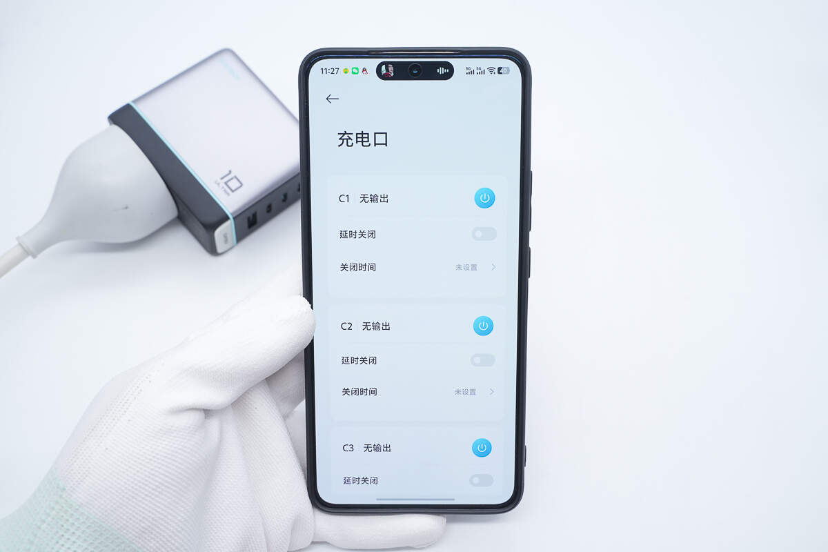
It also allows control of the power on/off status of each port, preset charging times, and scheduled power-off to help protect battery health.
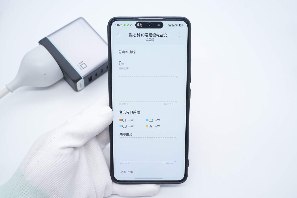
It also provides access to charging data for each port, power curves per port, as well as an overall power output curve.
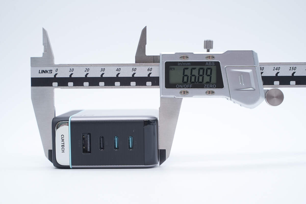
The length is about 66.89 mm (2.63 inches).
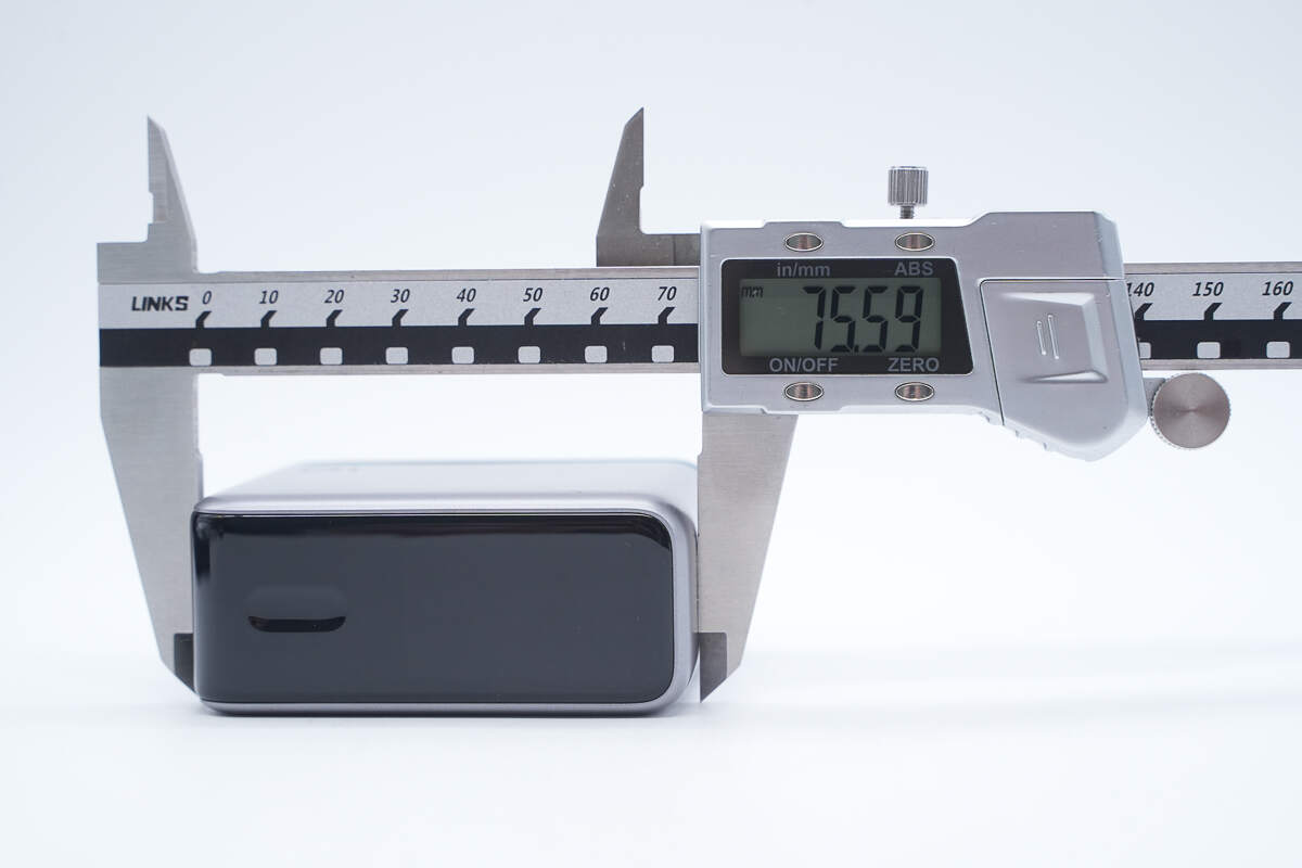
The width is about 75.59 mm (2.98 inches).
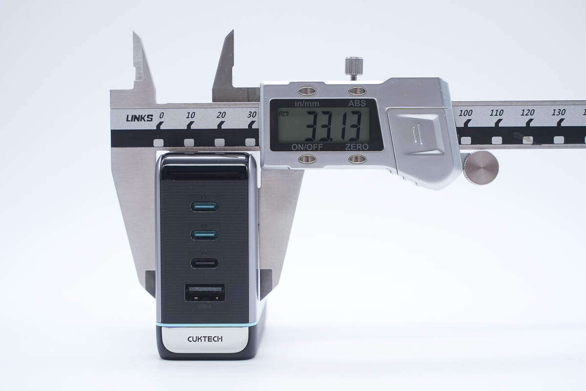
The thickness is about 33.13 mm (1.3 inches).
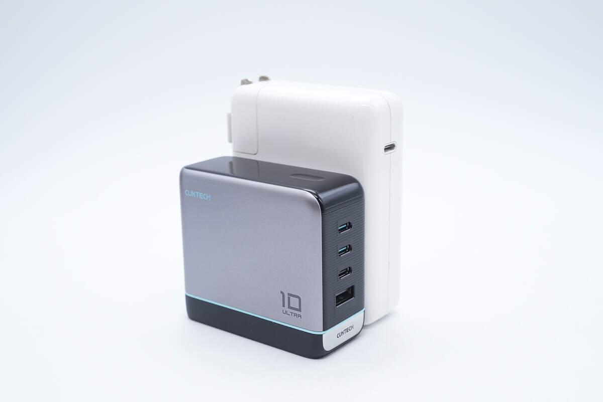
It is smaller than the Apple 140W charger.
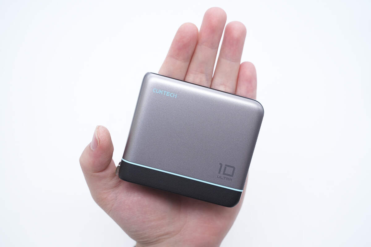
That's how big it is in the hand.
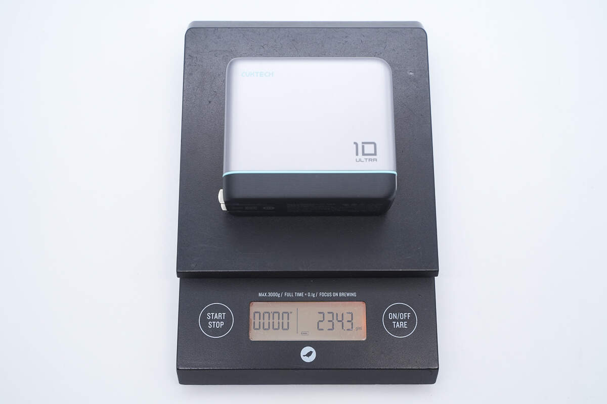
The weight is about 234 g (8.25 oz).
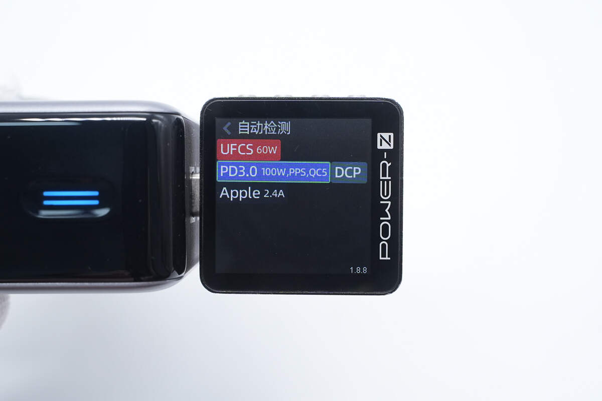
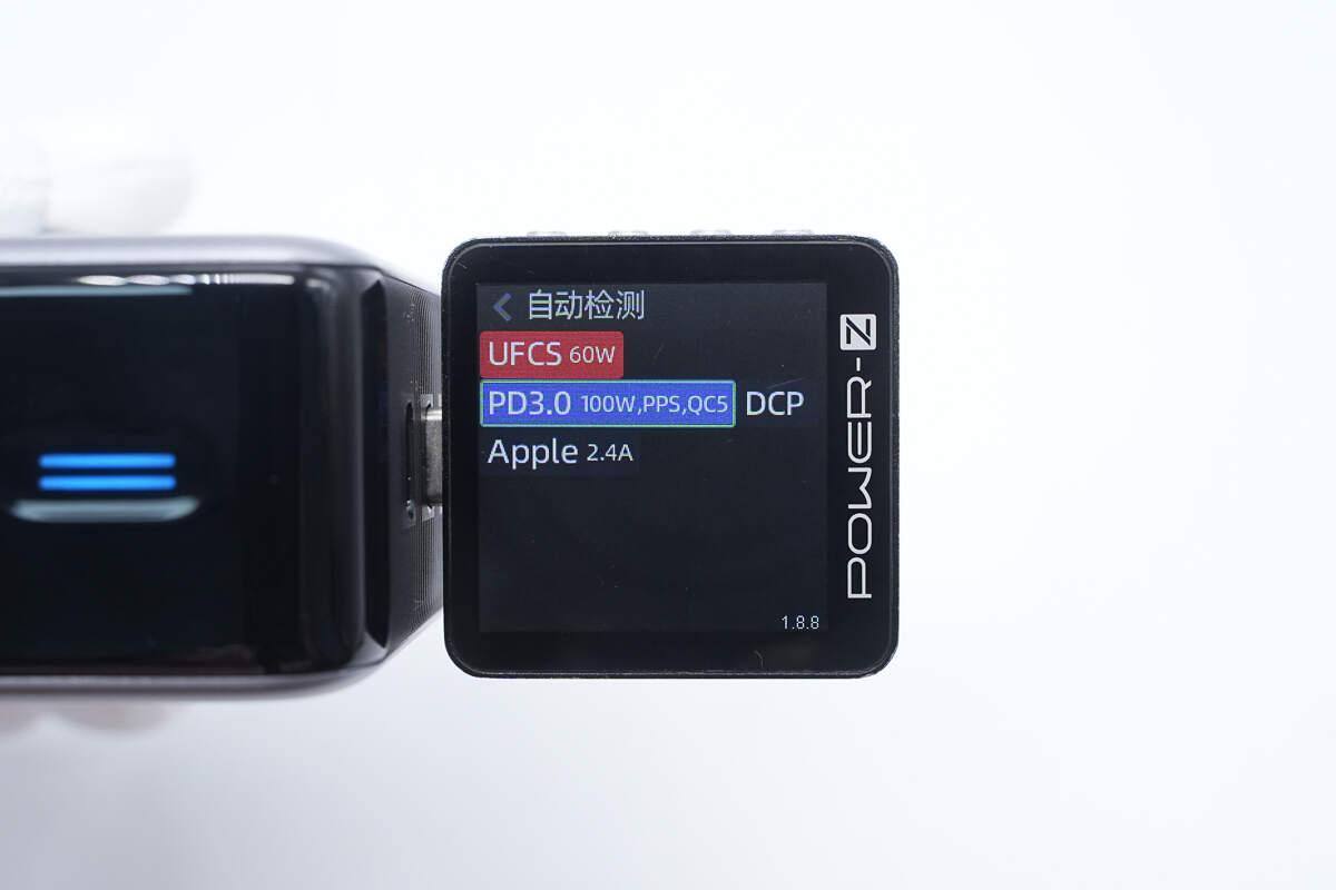
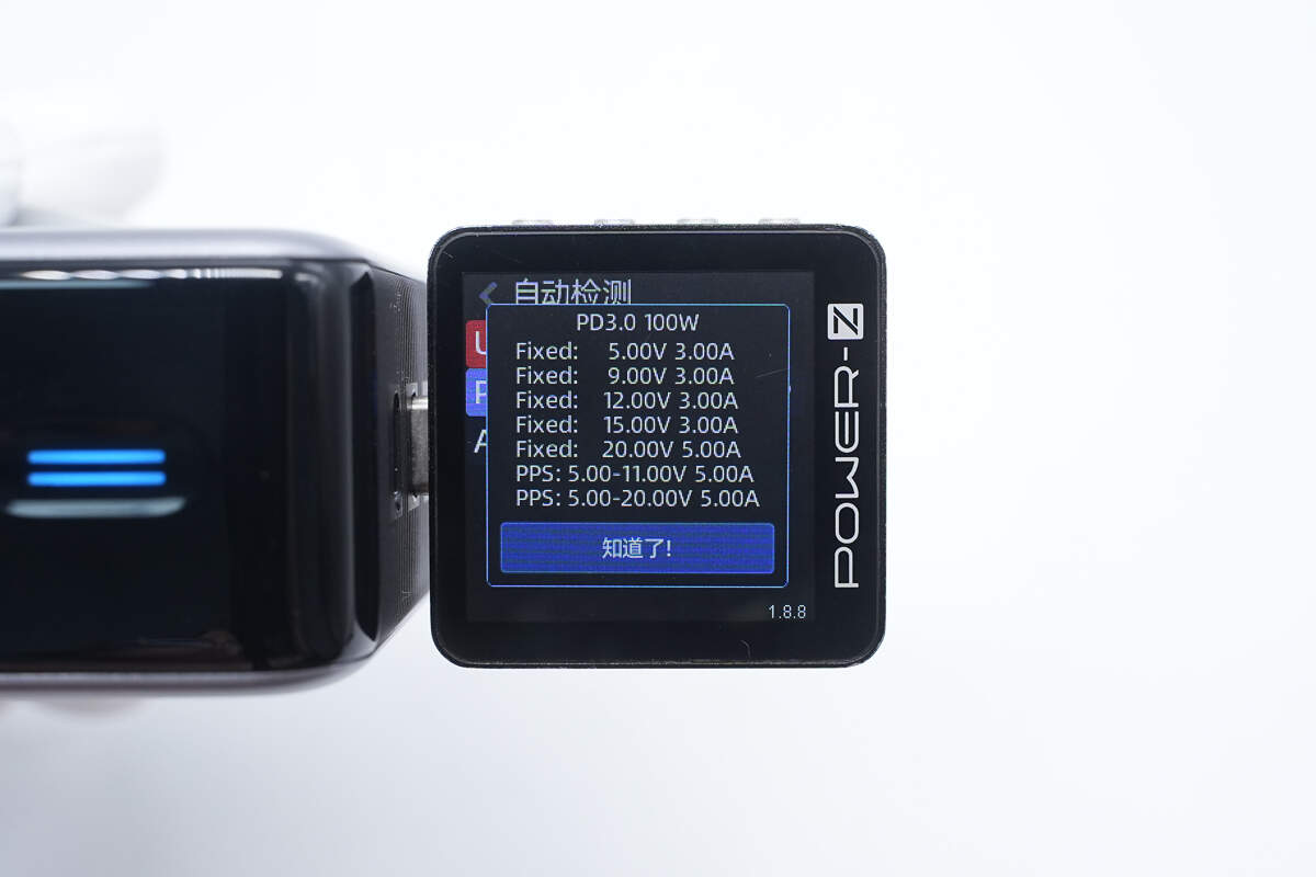
ChargerLAB POWER-Z KM003C shows the USB-C1 can support UFCS, PD3.0, PPS, QC5, DCP, and Apple 2.4A charging protocols.
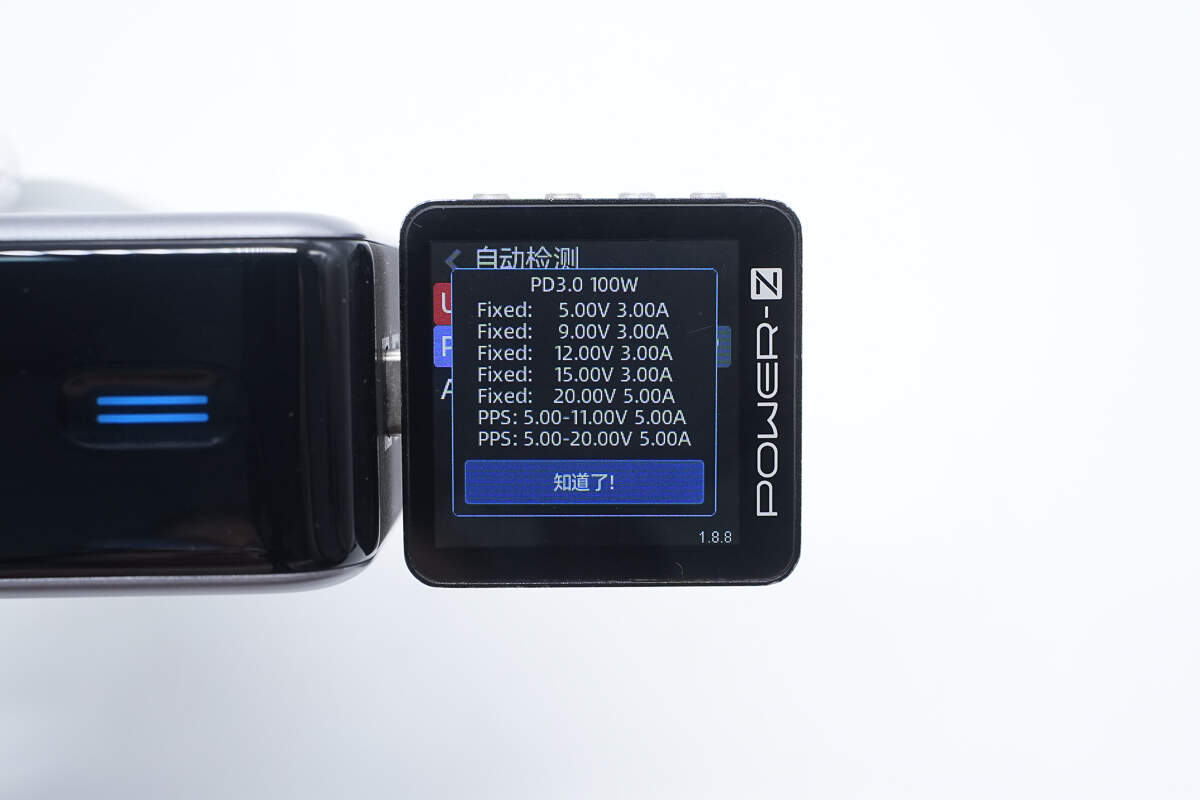
And it has five fixed PDOs of 5V3A, 9V3A, 12V3A, 15V3A, and 20V5A. It has two sets of PPS, which are 5-11V5A and 5-20V5A.
The protocols supported by USB-C2 are the same as those supported by USB-C1.
The PDOs are also identical.
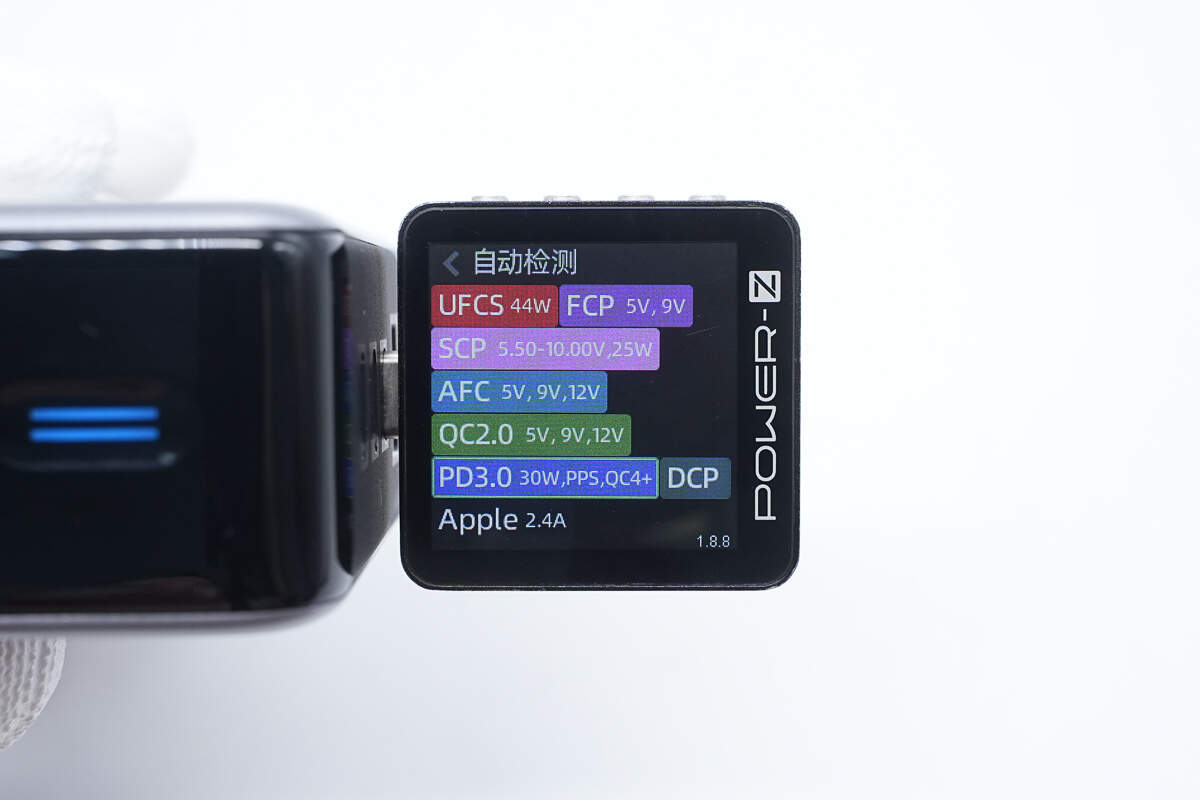
The USB-C3 can support UFCS, FCP, SCP, AFC, QC2.0/4+, PD3.0, PPS, DCP, and Apple 2.4A charging protocols.
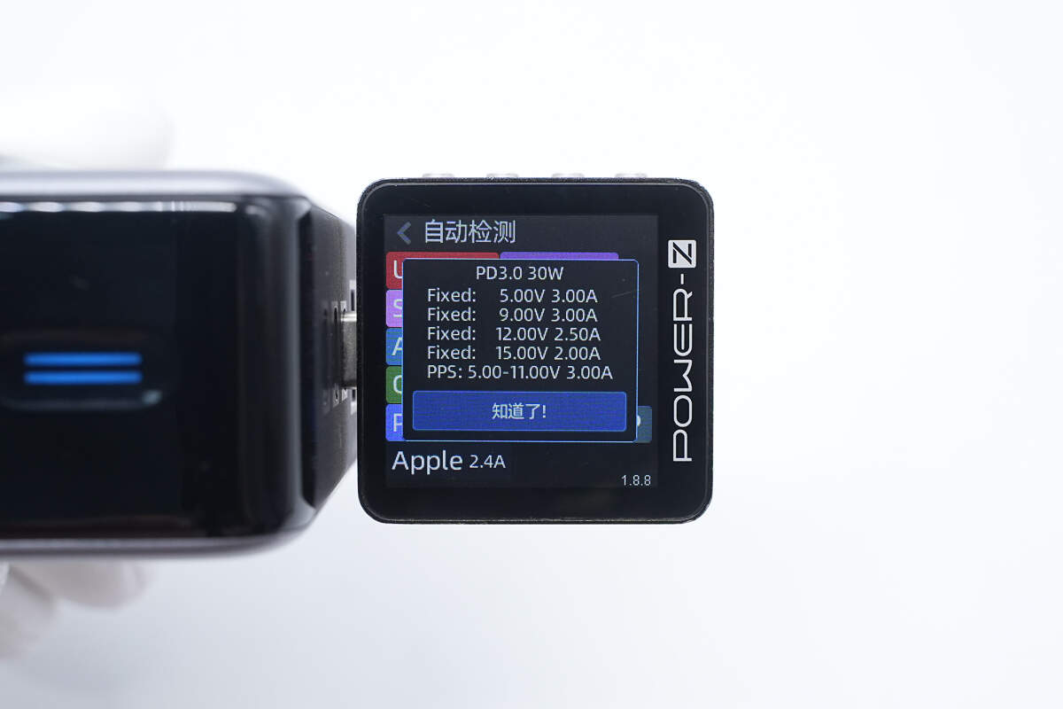
It has four fixed PDOs of 5V3A, 9V3A, 12V2.5A, and 15V2A. It has one set of PPS, which is 5-11V3A.
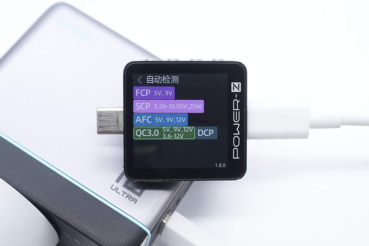
The USB-A can support FCP, SCP, AFC, QC3.0, and DCP charging protocols.
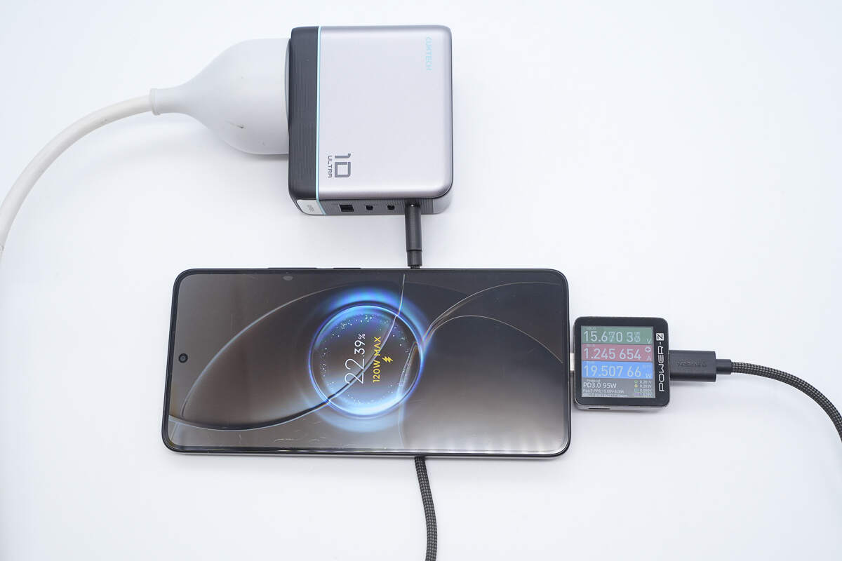
When charging the Redmi K80 Pro via USB-C1, the Xiaomi 120W proprietary fast-charging protocol is successfully activated.
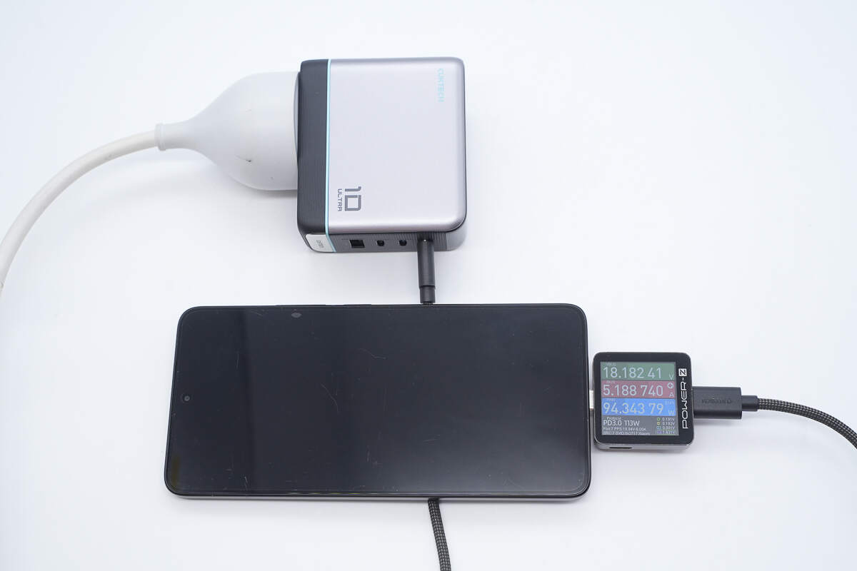
When the charging power is stable, the power is about 94.34W.
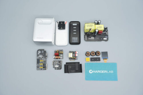
Teardown
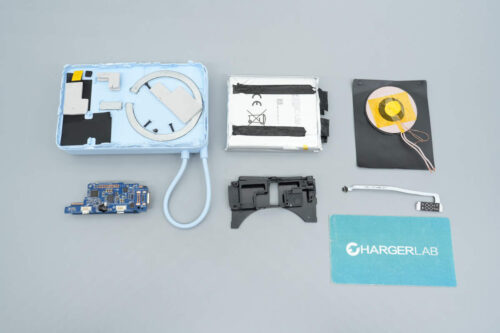
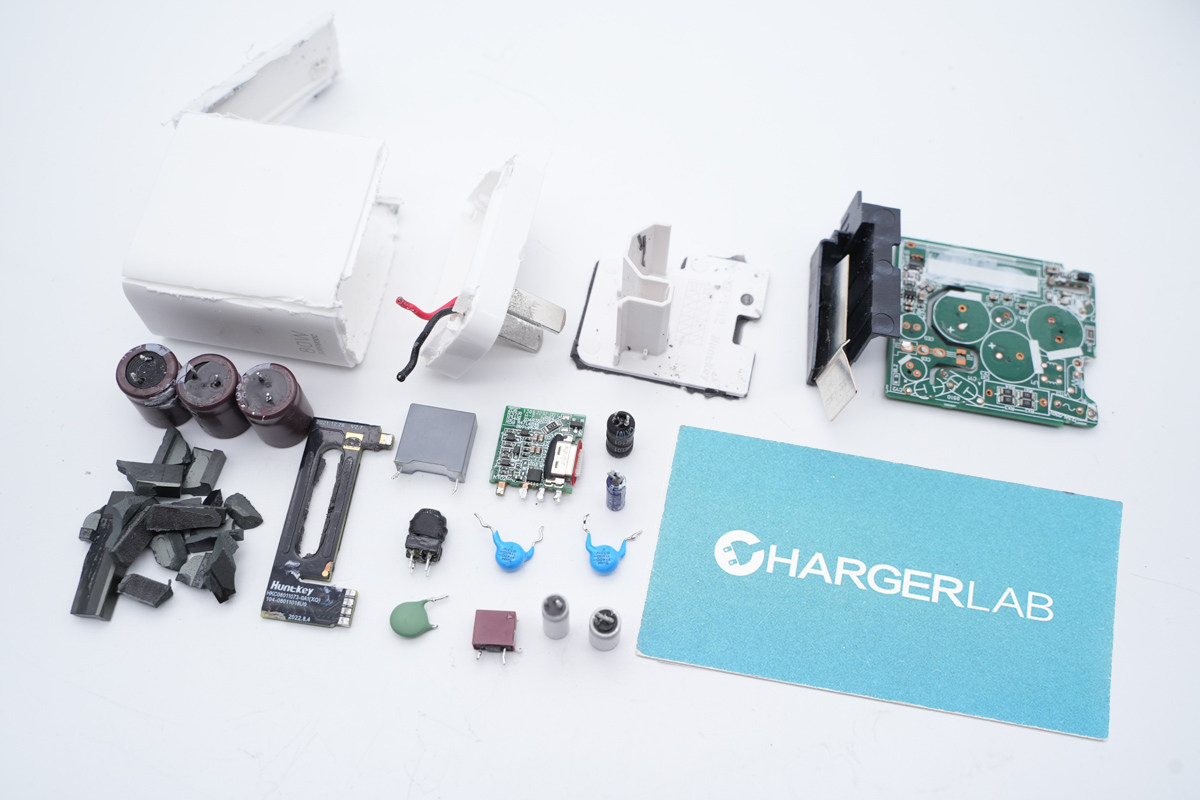
Next, let's take it apart to see its internal components and structure.
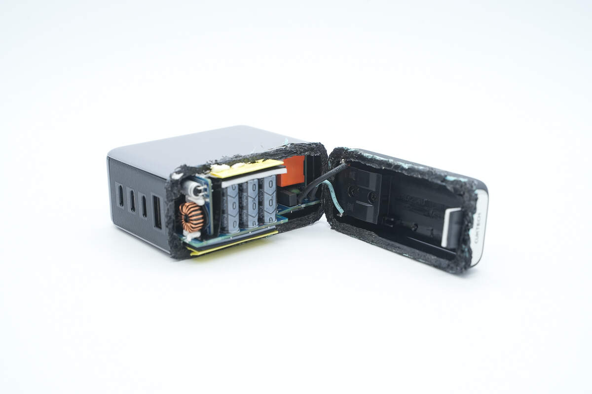
The bottom casing is cut open, and the prongs are connected to the PCBA module via wires.
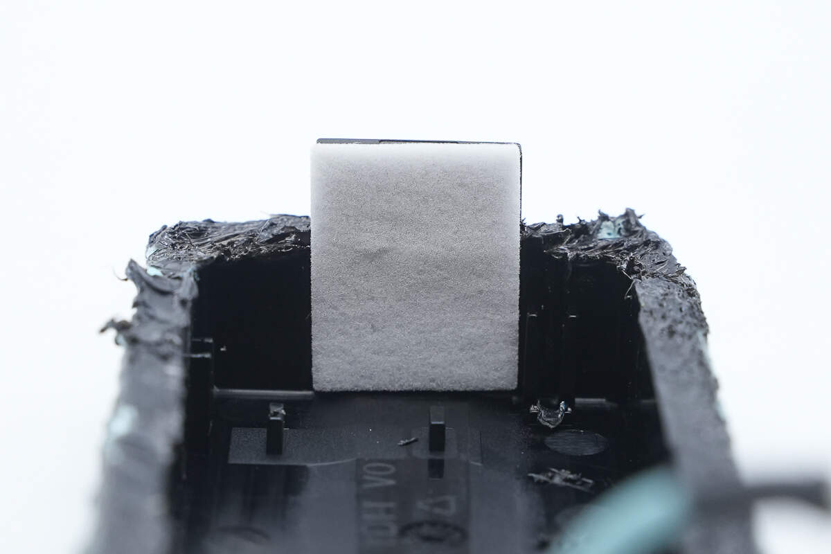
A piece of foam is attached to the inner side of the input-end casing.
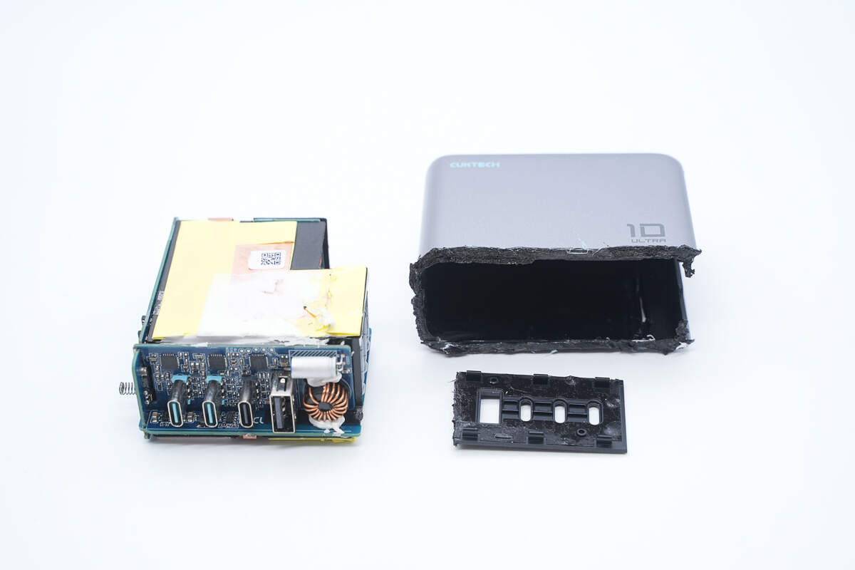
Take out the PCBA module.
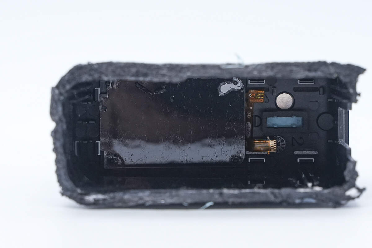
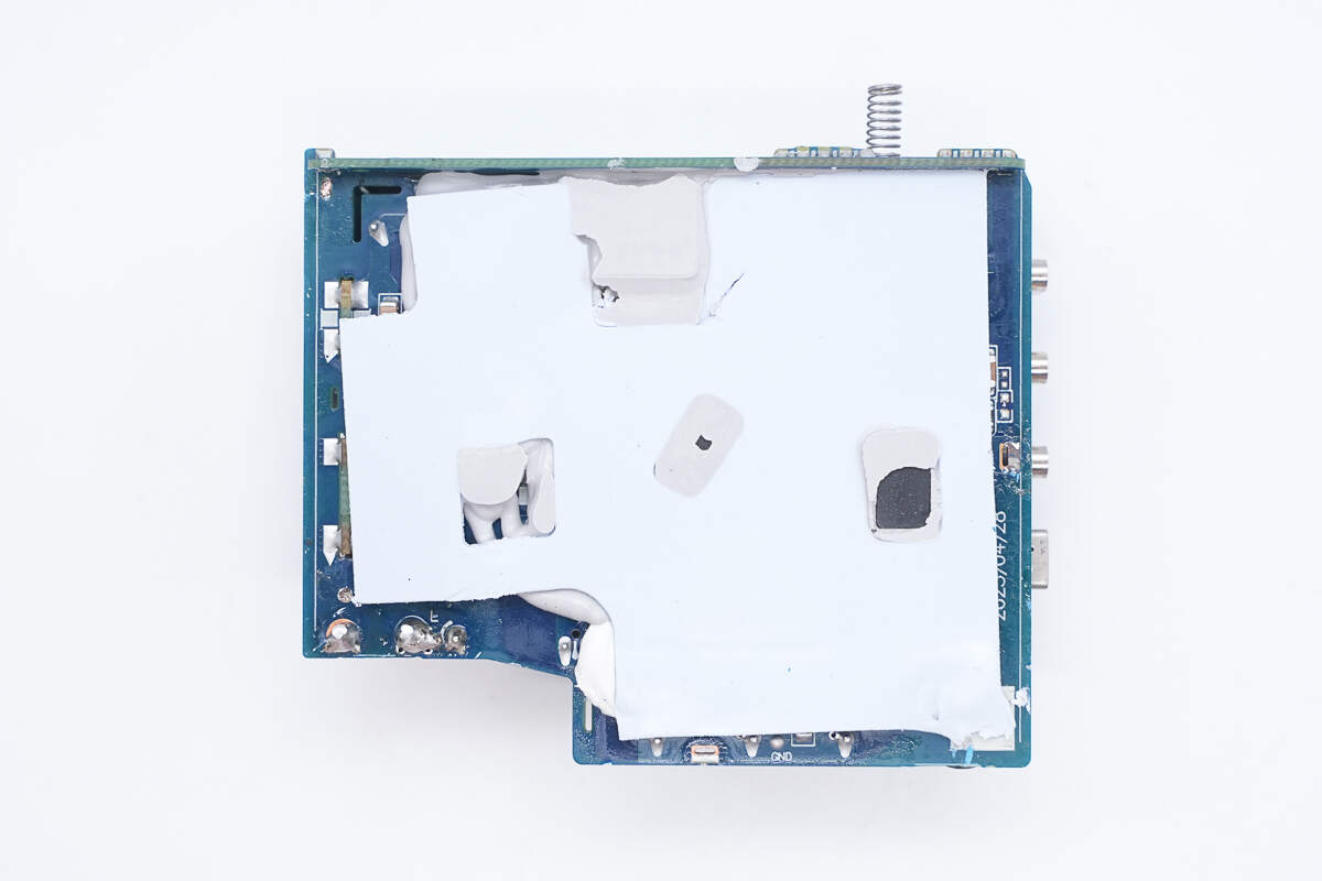
The screen is mounted on the inner side of the casing and connected to the PCBA module via a ribbon cable.
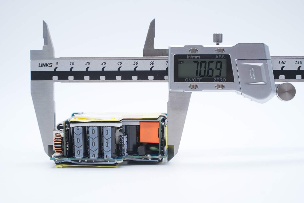
The length of the PCBA module is about 70.69 mm (2.78 inches).
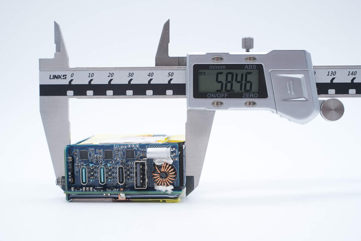
The width is about 58.46 mm (2.3 inches).
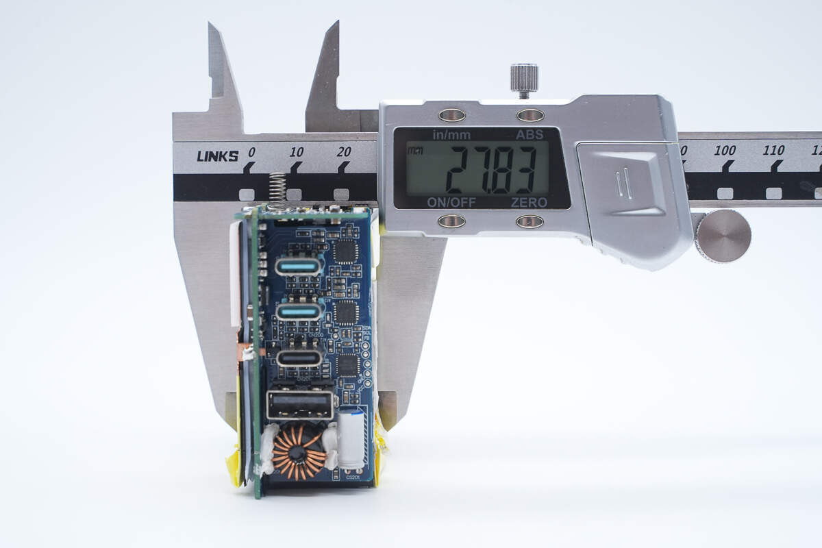
The thickness is about 27.83 mm (1.096 inches).
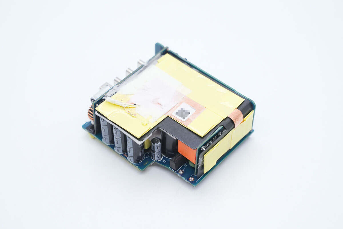
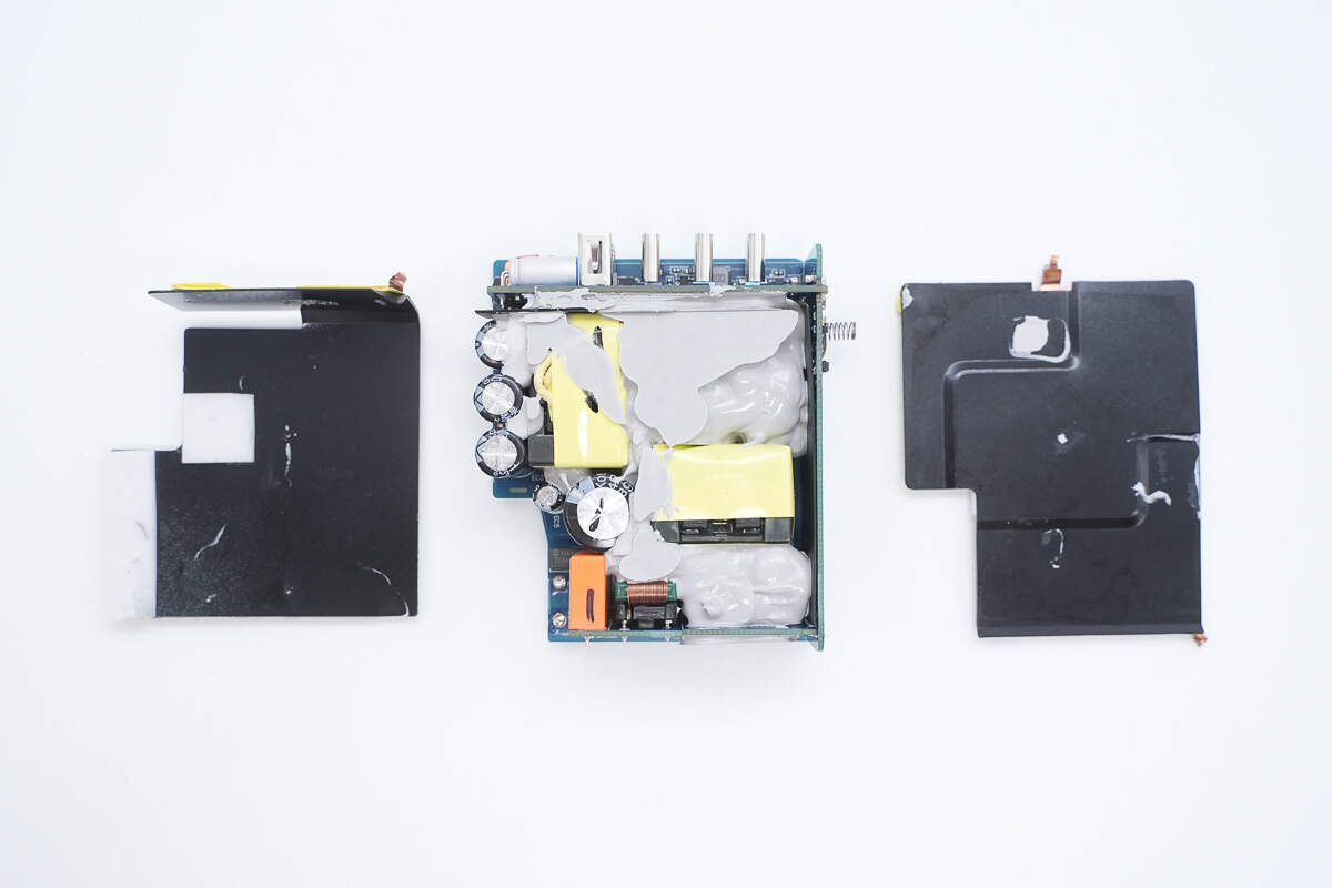
The top and one side of the PCBA module are covered with an integrated copper heatsink, wrapped with insulating tape, and attached with foam for protection.
The bottom is also covered with a copper heatsink, along with insulating tape and foam padding.
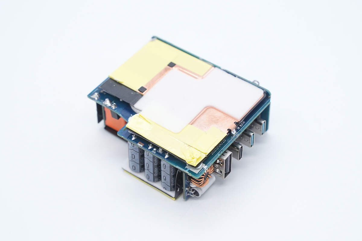
After removing the heatsinks, Mylar sheets are found on the inner side for insulation and isolation.
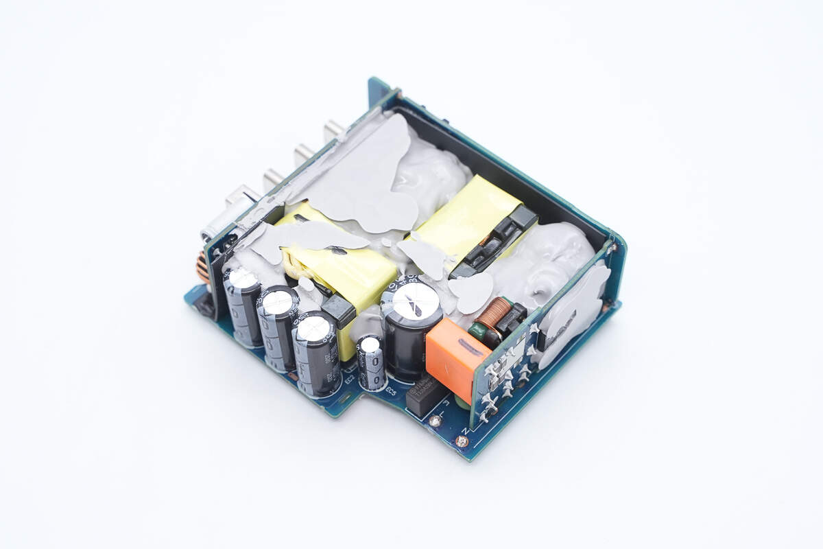
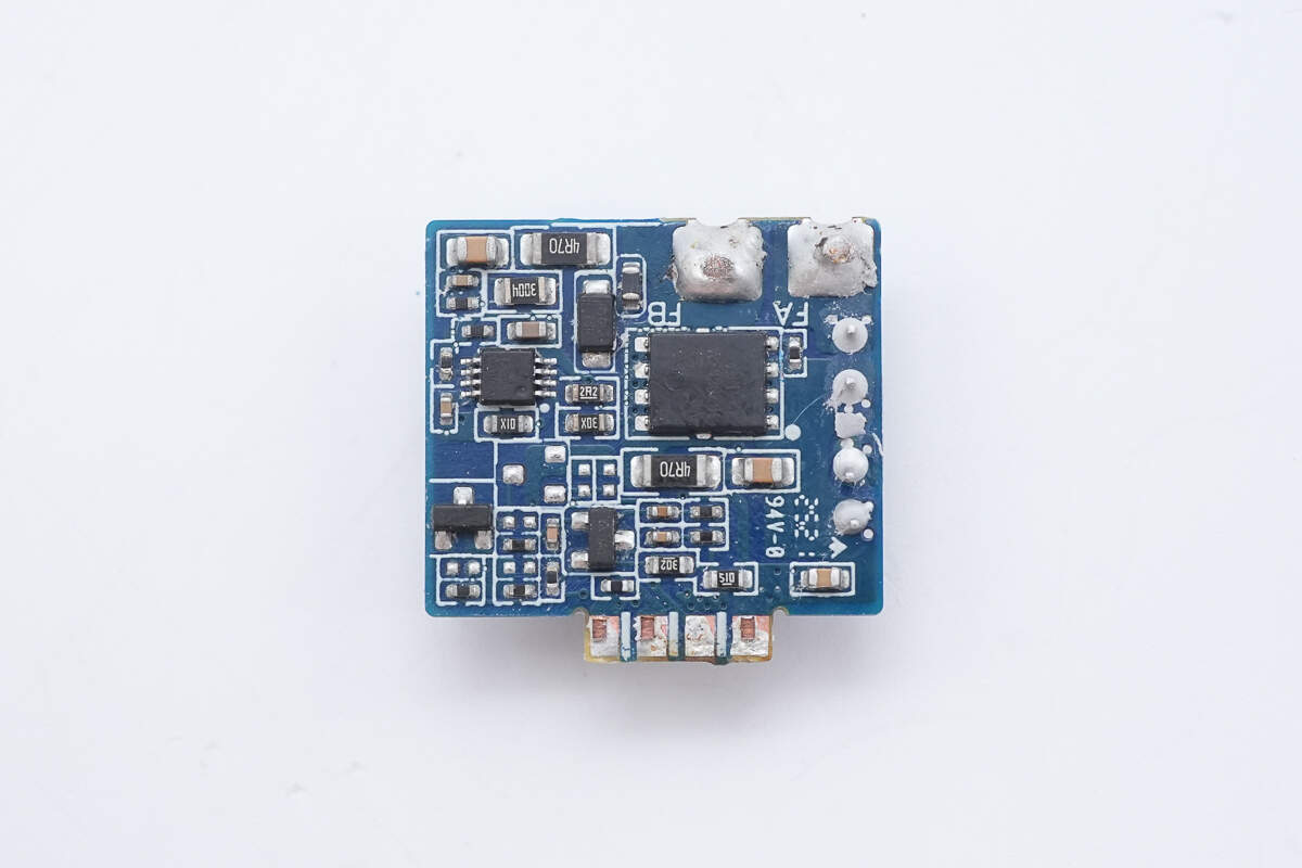
The module has three sides with small PCBs, and the main PCB area is filled with gray potting compound to aid heat dissipation.
The bottom is covered with a thermal pad and potting compound to transfer heat from the core heating chips.
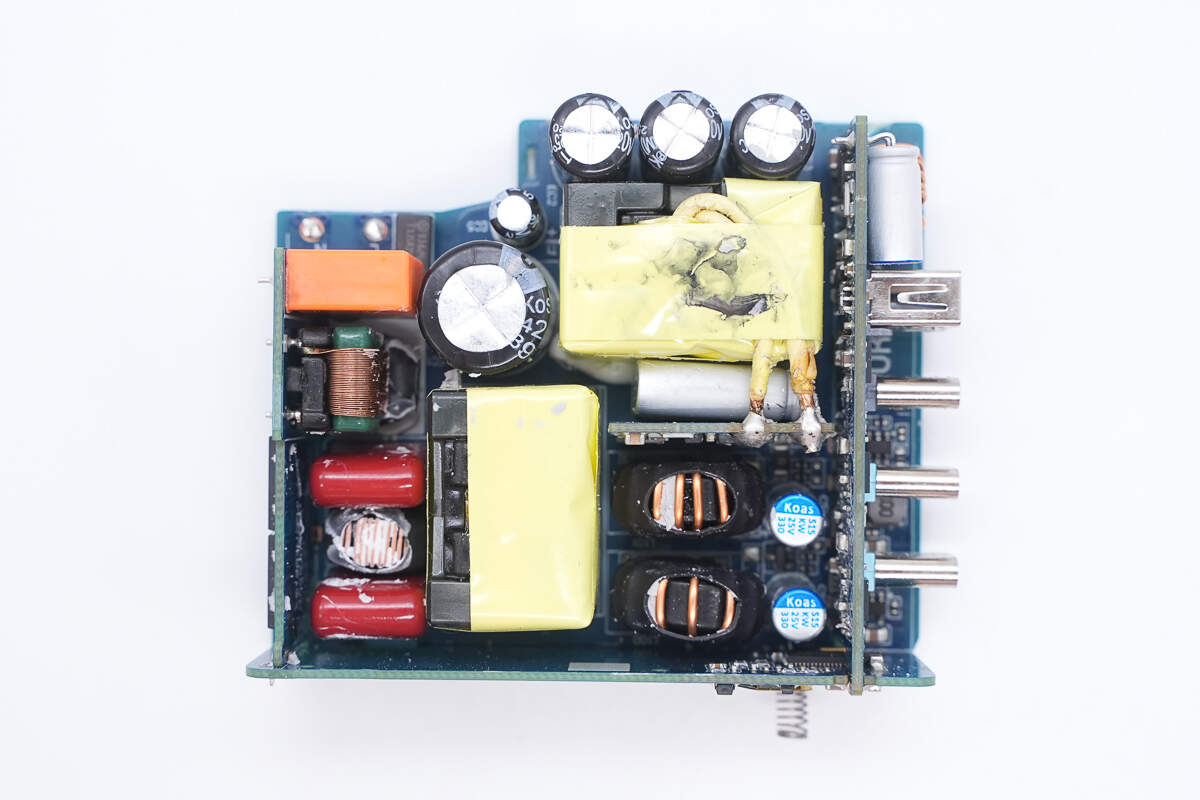
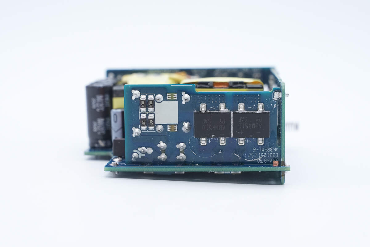
After removing the potting compound, the front side reveals components such as time-delay fuses, film capacitors, filter inductors, PFC boost inductors, electrolytic capacitors, transformers, as well as buck inductors and solid capacitors corresponding to the secondary step-down output circuits for the USB-C1 and C2 ports. Synchronous rectification PCBs are located next to the transformers and are soldered to the multi-layer insulated secondary windings.
On the back side, the left area houses the PFC boost circuitry, including PFC controllers, PFC MOSFETs, and PFC rectifiers. In the lower section, there is a master control chip. In the upper-right corner, the secondary step-down output circuits for the USB-C1 and C2 ports include synchronous buck controllers and synchronous buck MOSFETs.
There are two bridge rectifiers on the back side of the small PCB on this side.
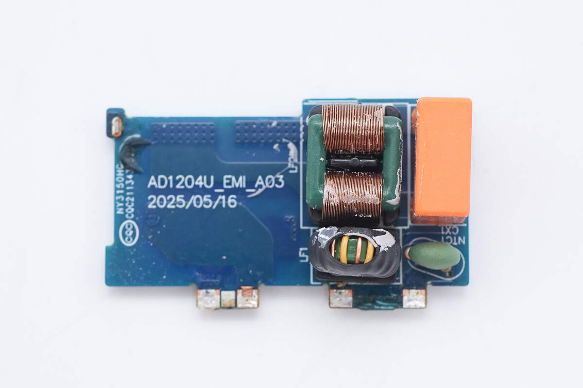
After removing the small PCB, the front side reveals an NTC thermistor, a safety X2 capacitor, and two common mode chokes.
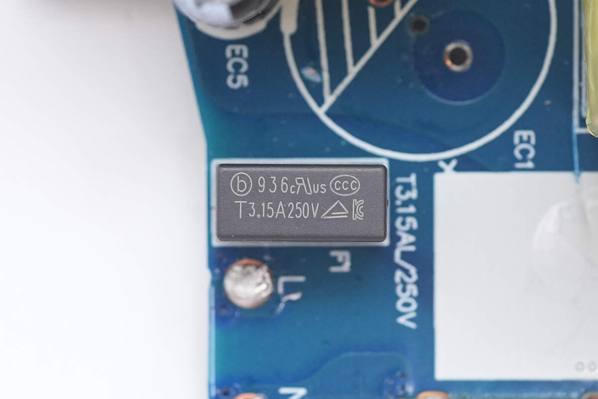
The time-delay fuse is from Betterfuse, with part number 936. 3.15A 250V.
The NTC thermistor is used to suppress inrush current during power-on.
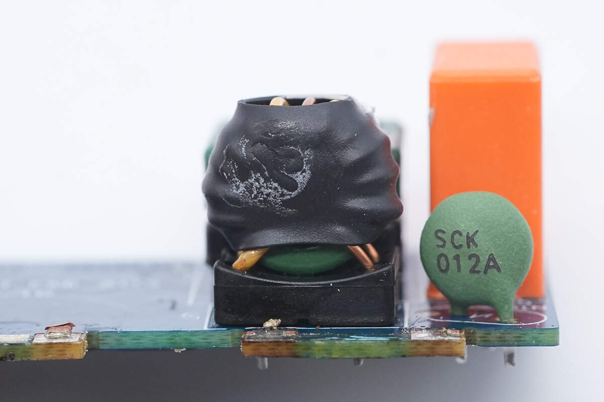
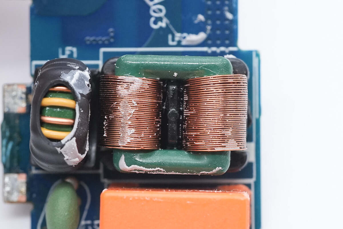
The common mode choke is insulated by heat-shrinkable tubing.
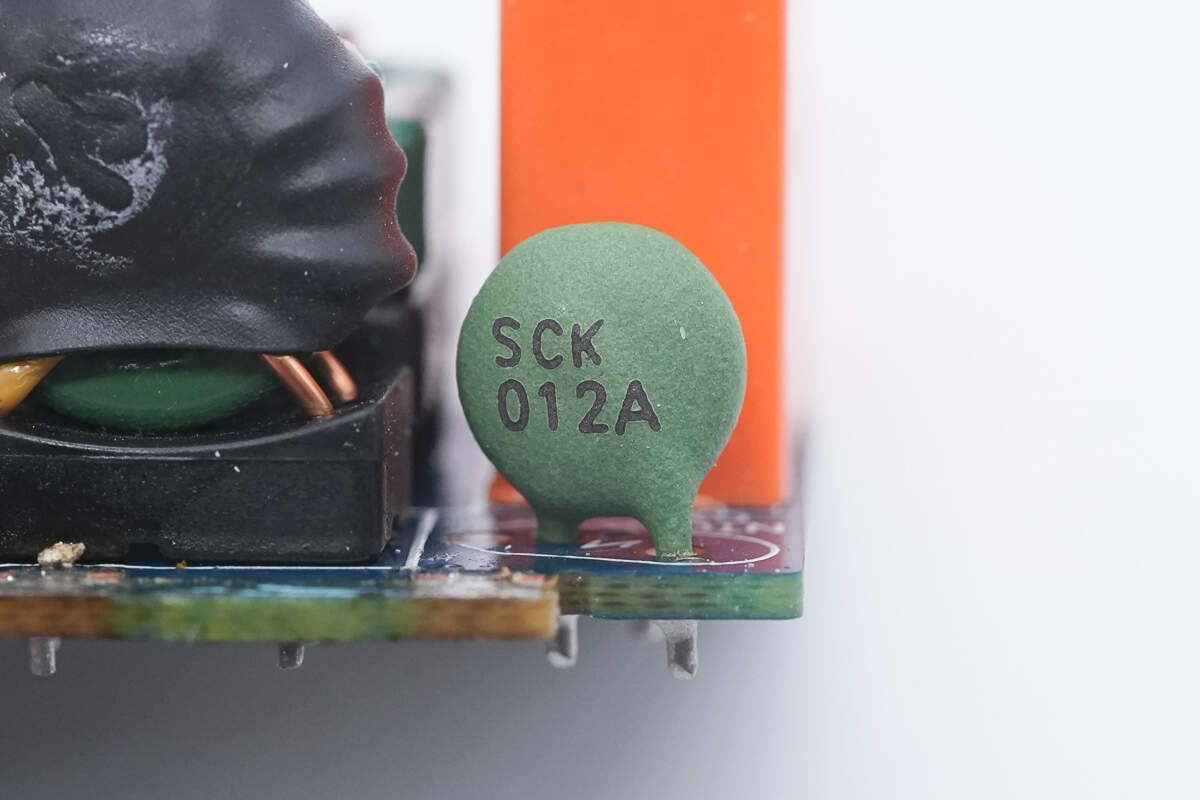
The safety X2 capacitor is from Surong. 0.33μF.
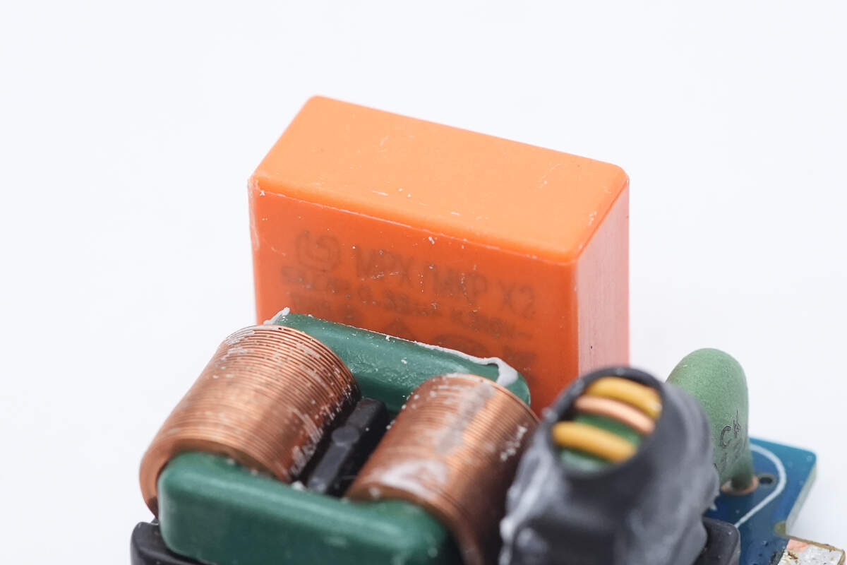
The other common mode choke is wound with flat copper strips, and its two-stage design provides improved EMI suppression.
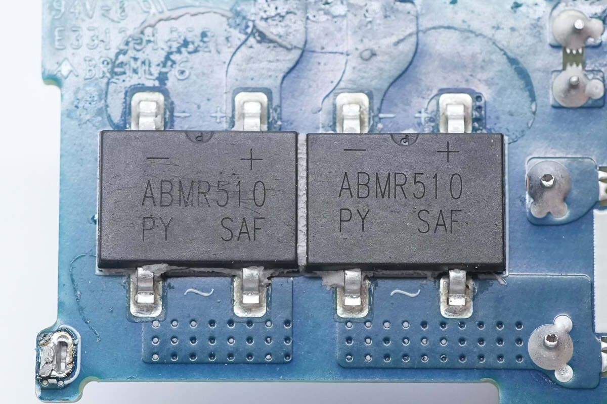
The two bridge rectifiers are from Pingwei, model ABMR510, with ABM package. 5A 1000V.
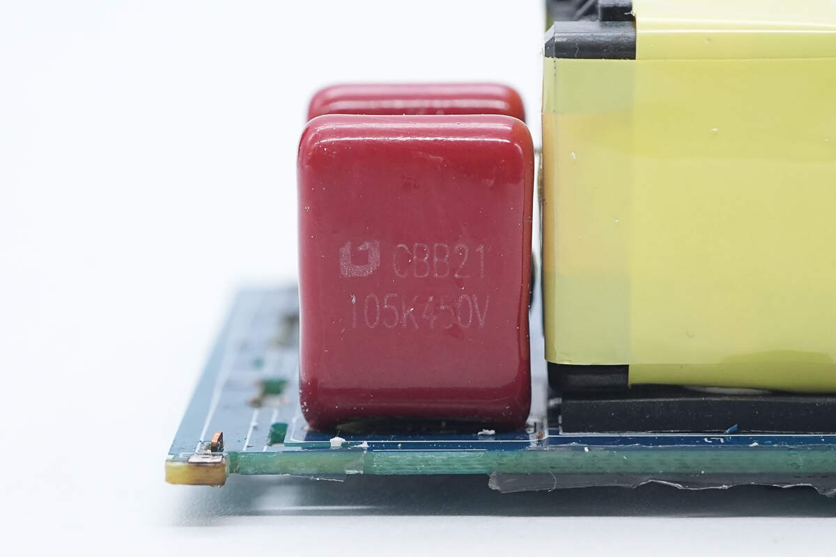
The two CBB21 film capacitors are also from Surong. 1μF 450V.
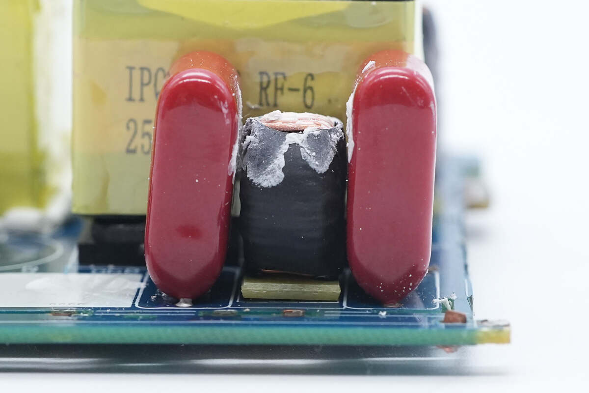
The filter inductor is insulated with heat-shrink tubing and bakelite.
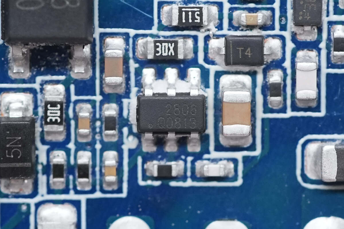
The PFC boost controller is the KP2806 from Kiwi Instruments, a high-performance quasi-resonant (QR) boost-type constant-voltage PFC controller that can adaptively operate in critical conduction mode (CRM) and discontinuous conduction mode (DCM).
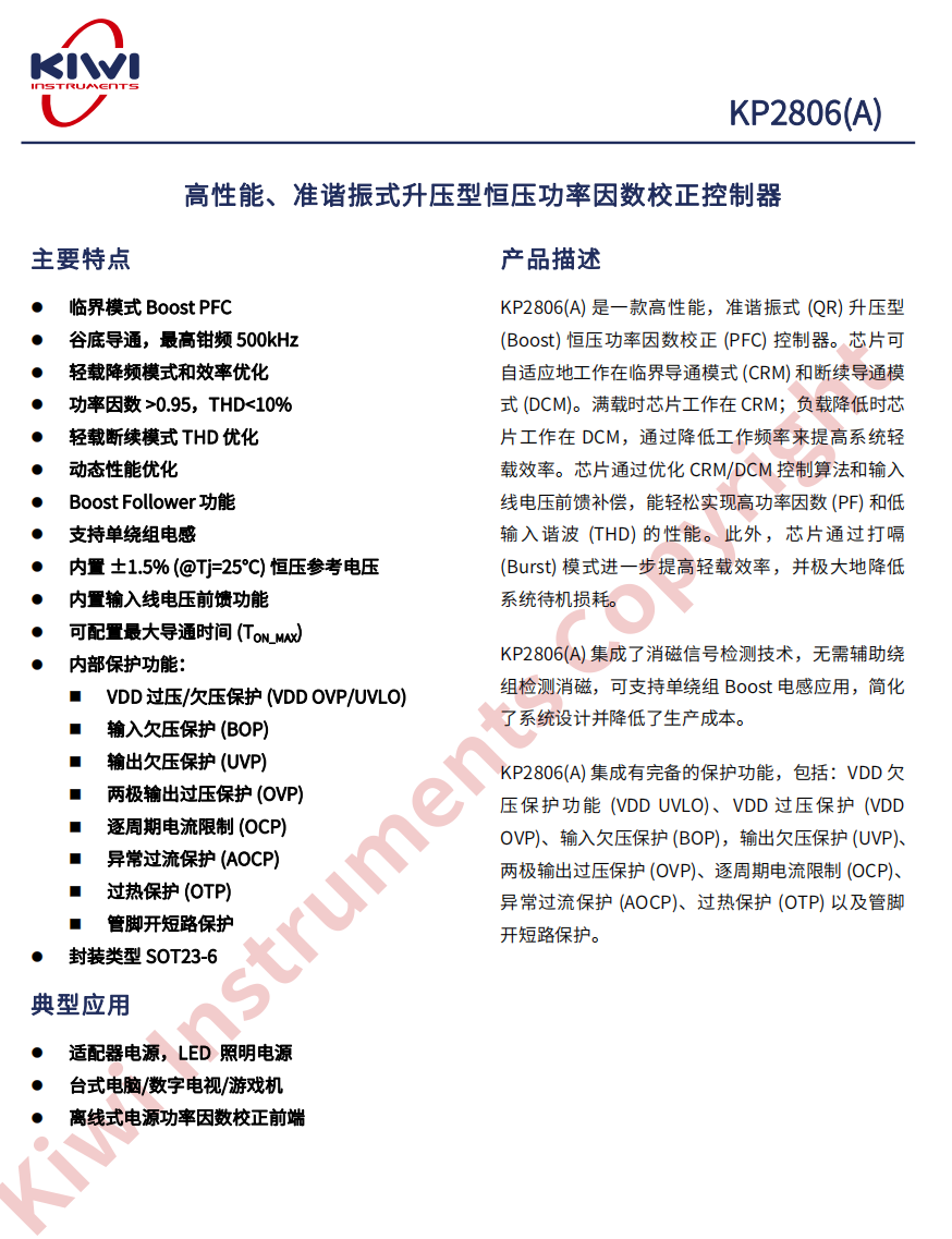
The KP2806 uses a SOT23-6 package and features multifunctional pin multiplexing, achieving a compact and efficient design. This allows for reduced PCB footprint, enabling smaller overall size and lower design cost.
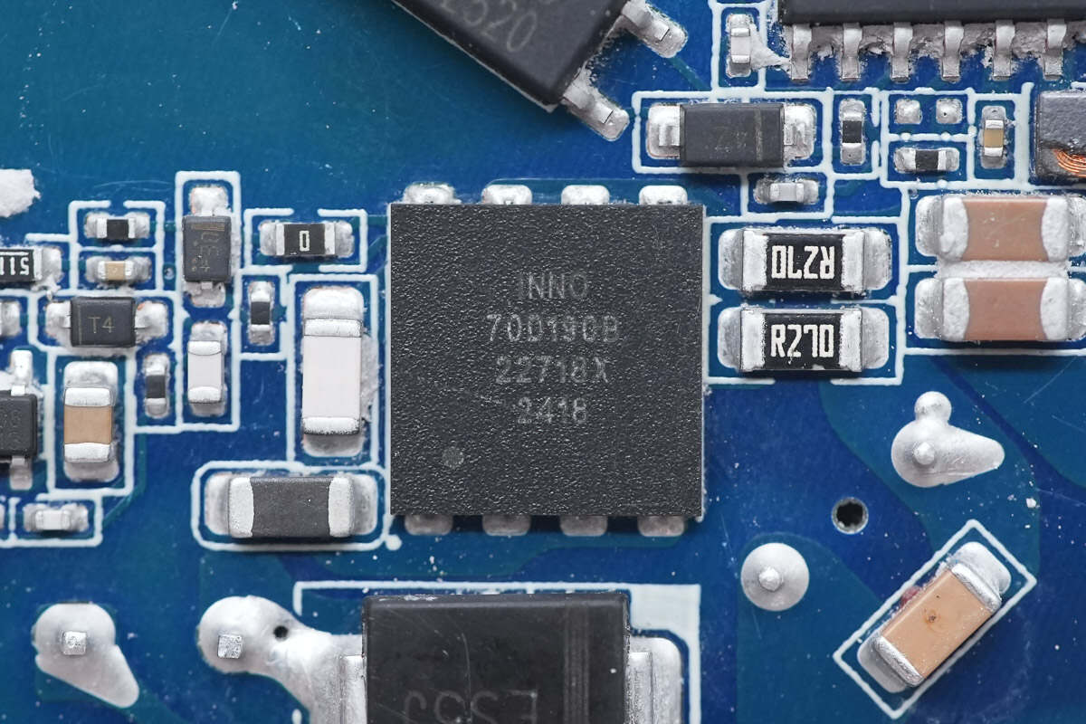
The PFC MOSFET is the Innoscience INN700D190B, an enhancement-mode GaN device rated for 700 V. It is an upgrade from the previous 650 V version, with a transient voltage tolerance of up to 800 V. The device has an on-resistance of 190 mΩ and supports higher power applications.
The INN700D190B supports ultra-high switching frequencies and features zero reverse recovery charge, along with extremely low gate charge and output charge. It complies with JEDEC standards for industrial applications, includes built-in ESD protection, and meets RoHS, lead-free, and EU REACH requirements. It is well suited for high-efficiency, high-density applications such as AC-DC and DC-DC conversion. The device comes in a DFN8×8 package.
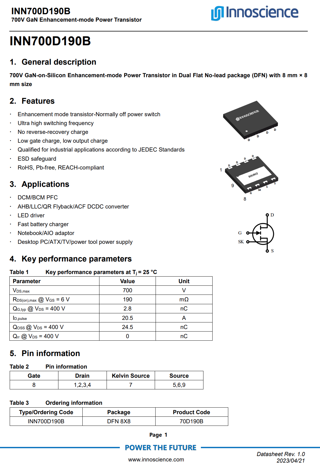
Here is the information about Innoscience INN700D190B.
Close-up of the PFC boost inductor.
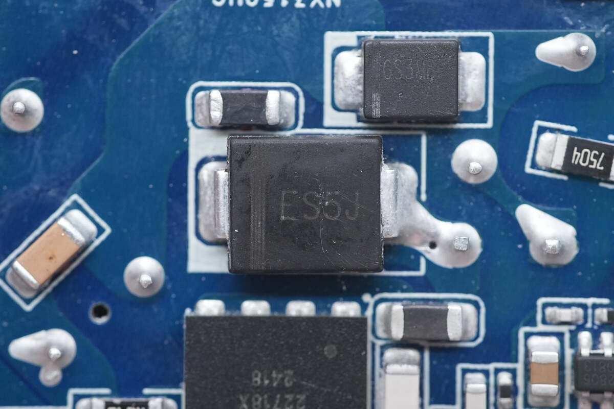
The PFC rectifier is the ES5J, an ultrafast recovery diode with a rating of 5 A and 600 V, housed in a DO-214AB SMD package.
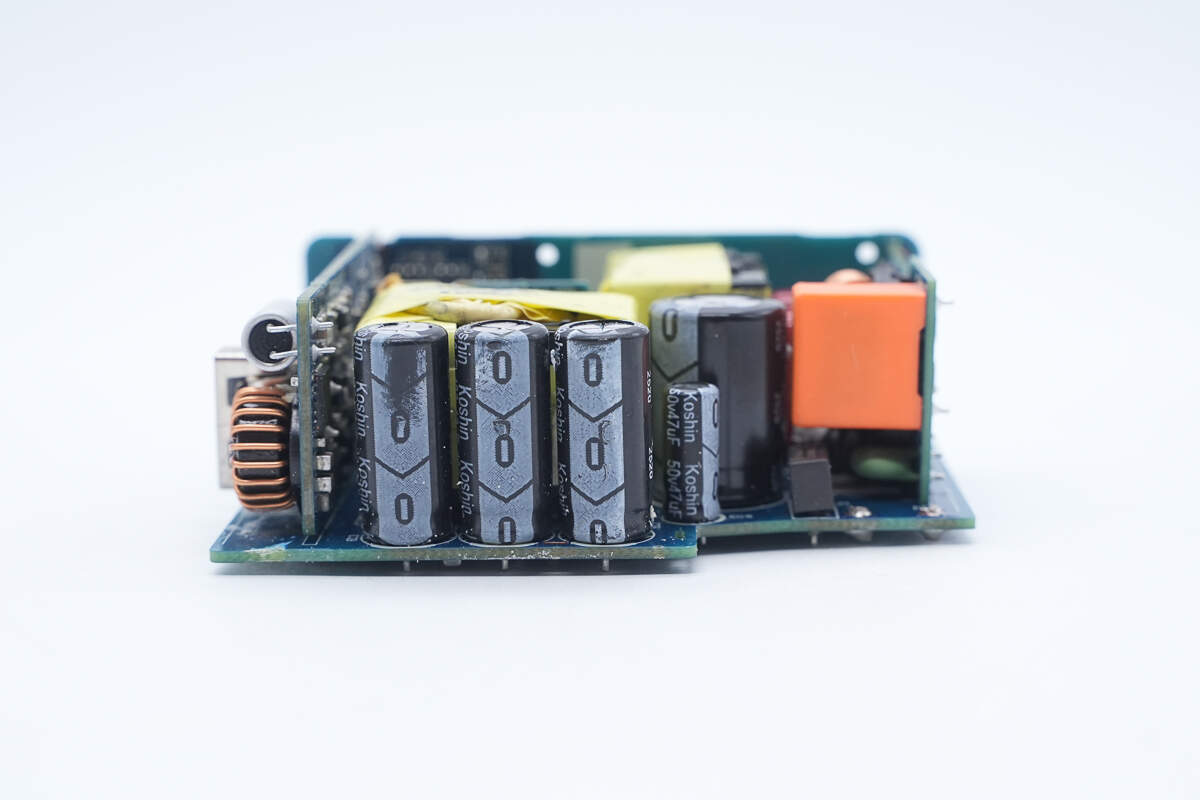
The front end of the module includes components such as electrolytic capacitors, a capacitor that supplies power to the master control chip, and the transformer.
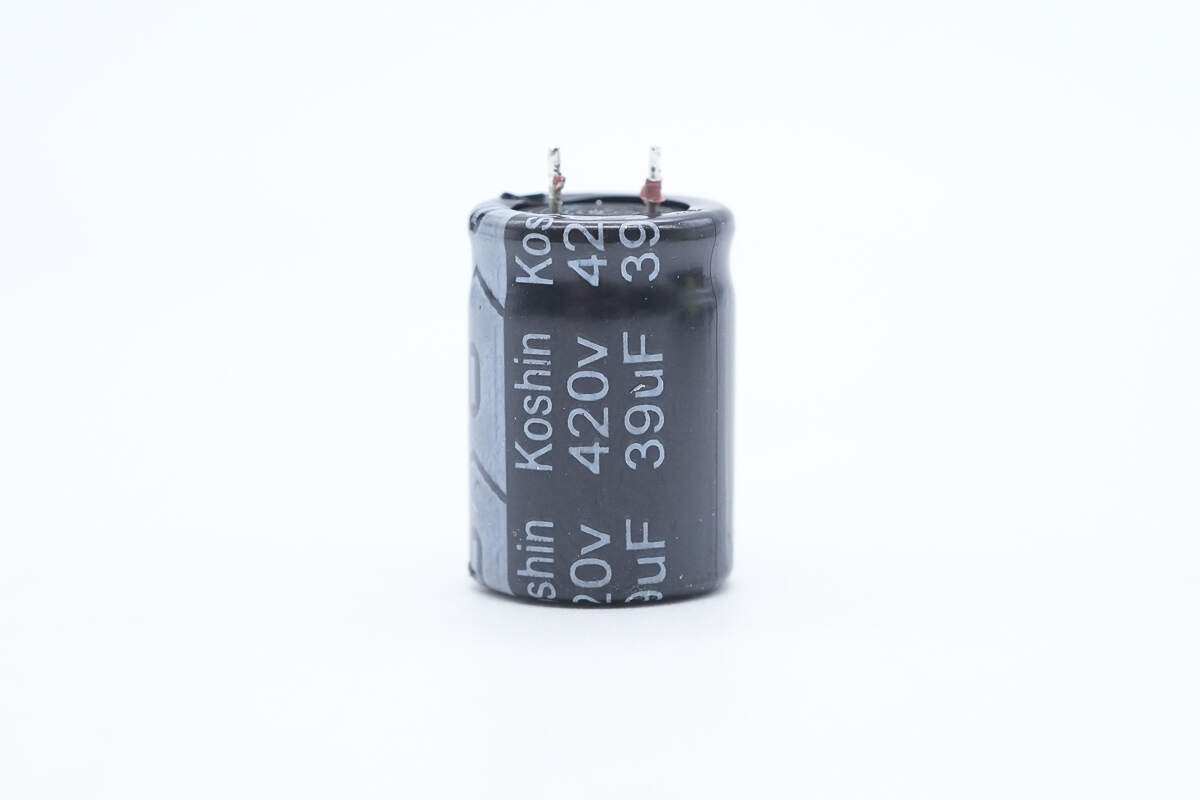
The electrolytic capacitor is from Koshin. 420V 39μF.
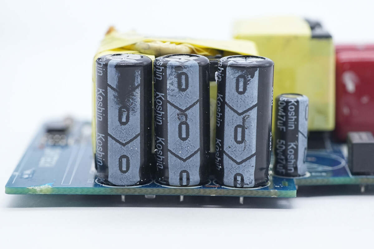
The other three electrolytic capacitors are also from Koshin.
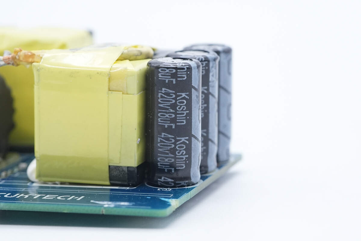
All have specifications of 420 V and 18 μF.
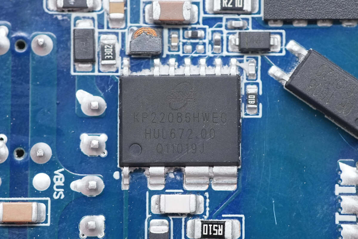
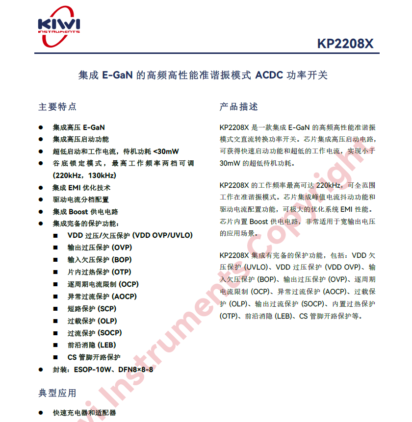
The master control chip is from Kiwi Instruments, model KP22086. It is a high-frequency, high-performance quasi-resonant AC-DC power switch integrated with E-GaN technology. The chip features an integrated high-voltage startup circuit, enabling fast startup and ultra-low operating current, achieving standby power consumption below 30 mW.
The KP2208X operates at frequencies up to 220 kHz and supports full-range quasi-resonant mode operation. It includes peak current jitter and drive current configuration functions, significantly optimizing system EMI performance. The chip also incorporates a built-in Boost power supply circuit, making it well suited for wide output voltage applications. Packaging options include ESOP-7 and ESOP-10W, meeting application requirements from 20 W to 120 W.
The KP2208X integrates comprehensive protection features, including VDD undervoltage lockout (UVLO), VDD overvoltage protection (VDD OVP), input undervoltage protection (BOP), output overvoltage protection (OVP), cycle-by-cycle overcurrent protection (OCP), abnormal overcurrent protection (AOCP), overload protection (OLP), secondary output overcurrent protection (SOCP), built-in over-temperature protection (OTP), leading-edge blanking (LEB), and CS pin open-circuit protection.
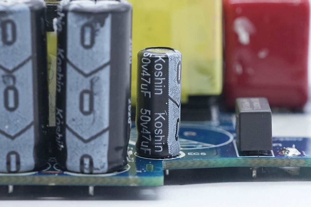
The capacitor that supplies power to the master control chip is also from Koshin. 50 V 47 μF.

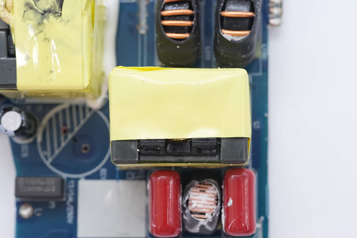
Close-up of the transformer.
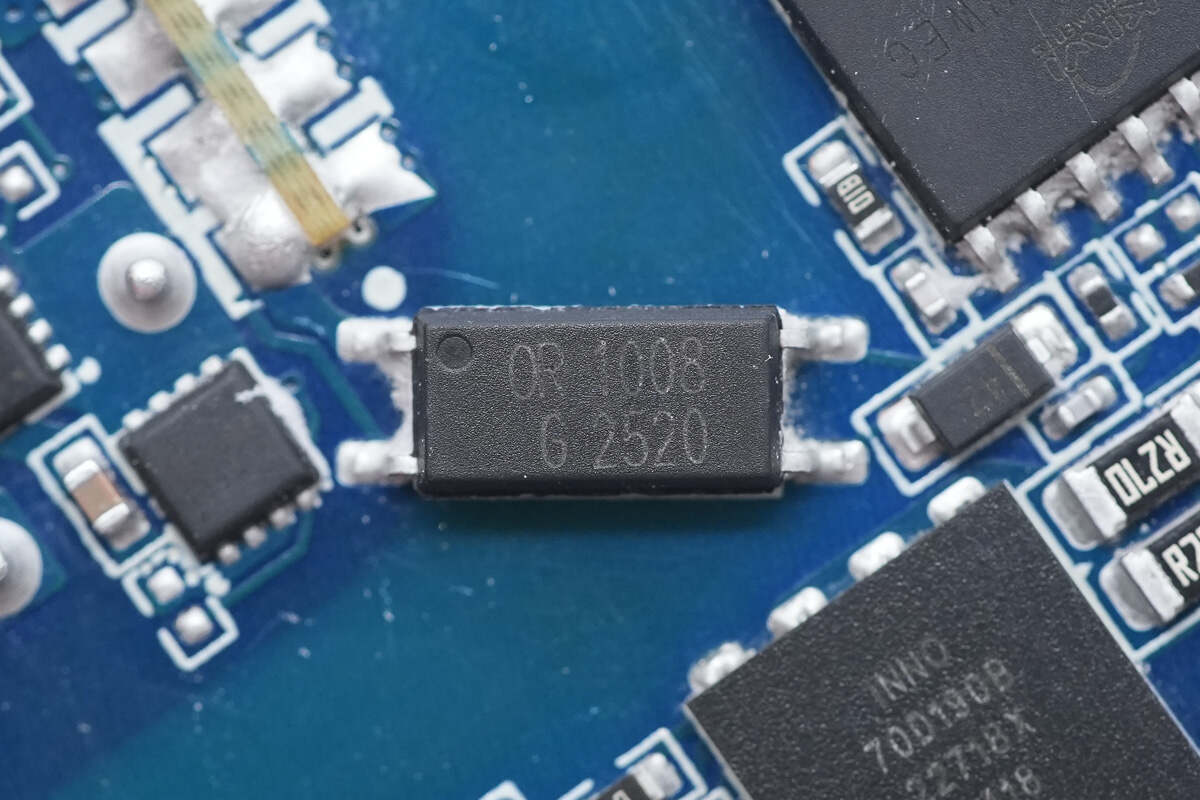
The OR 1008 optocoupler is used for output voltage feedback.
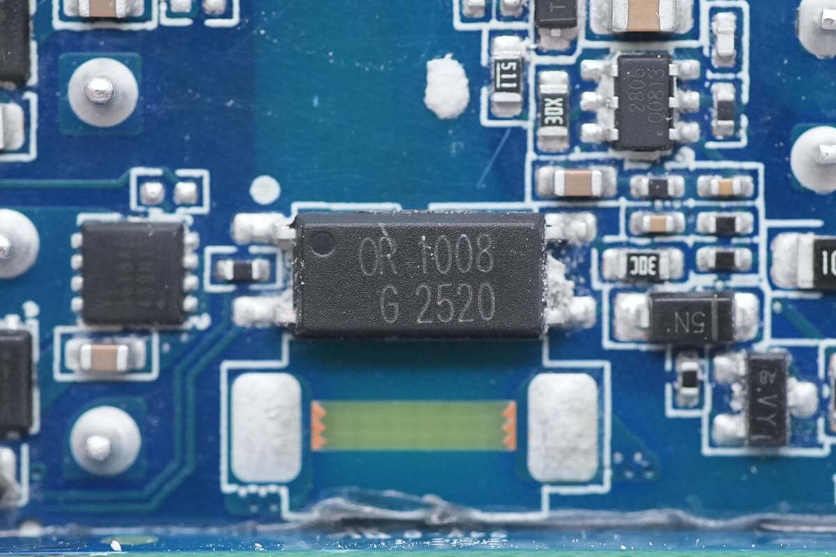
Close-up of the other OR 1008 optocoupler.
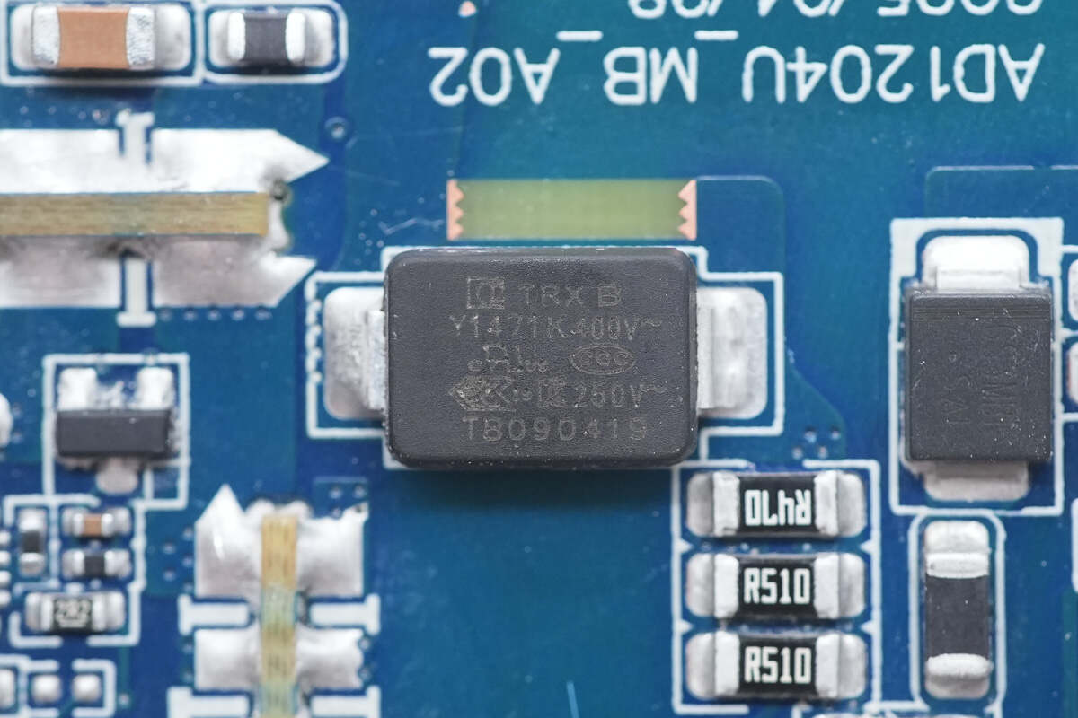
The SMD Y capacitor is from TRX. Its small size and light weight are suitable for high-density power products such as GaN fast chargers. The part number is TMY1471K.
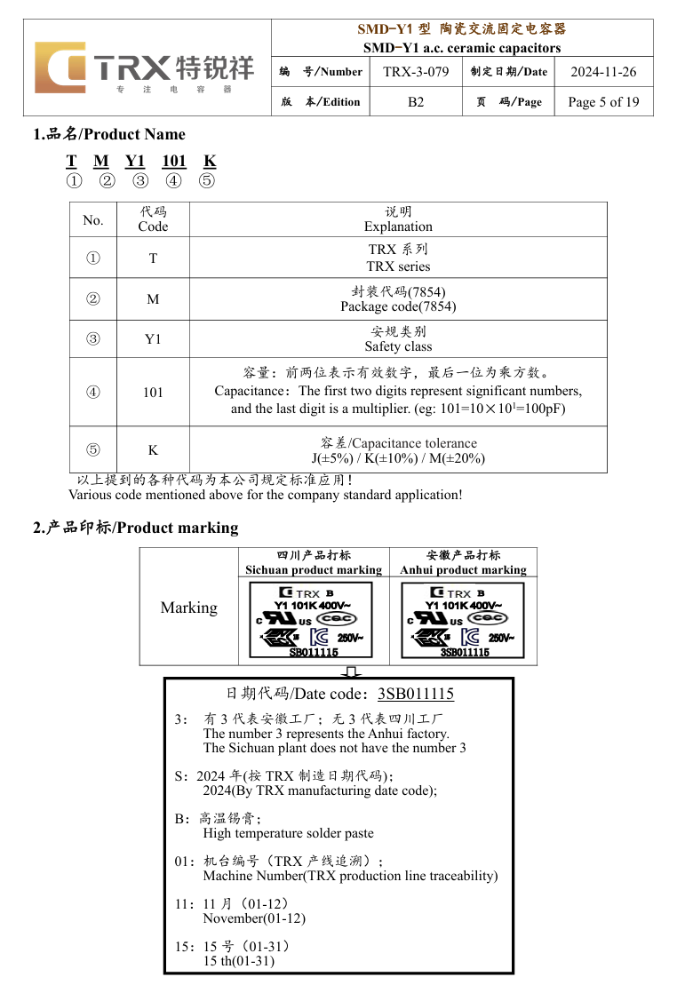
Here is the information about the SMD Y capacitor.
The small PCB connected to the transformer features two solid capacitors for output filtering on its front side.
The back side has a synchronous rectifier controller and a synchronous rectifier.
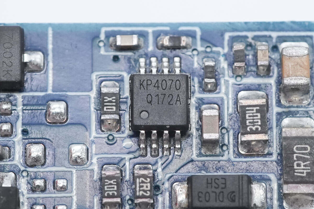
The synchronous rectifier controller is from Kiwi Instruments, model KP4070. It is a high-performance secondary-side synchronous rectifier controller designed to replace Schottky diodes in flyback converters—when used with an external MOSFET—to improve system efficiency.
The KP4070 supports ZVS on the primary side by coordinating with the primary-side MOSFET. It is recommended for use with Kiwi Instruments’ primary-side controller series KP2206X and KP2208X. After the secondary conduction period ends, the SR briefly turns on at the appropriate point in the resonance cycle to provide reverse excitation to the transformer. This enhances the resonance on the primary side, bringing the voltage across the primary MOSFET close to 0 V during turn-on, thereby enabling ZVS operation.
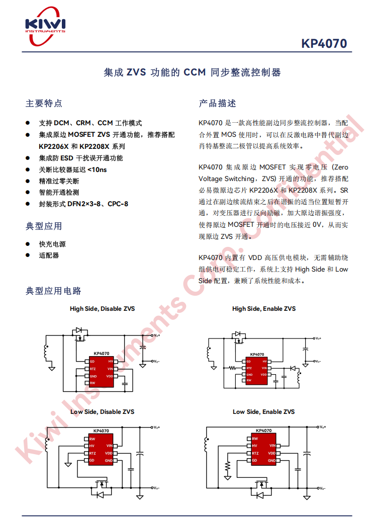
The KP4070 integrates a high-voltage VDD power supply module, allowing it to operate reliably without the need for auxiliary winding power. It supports both high-side and low-side configurations, balancing system performance and cost.
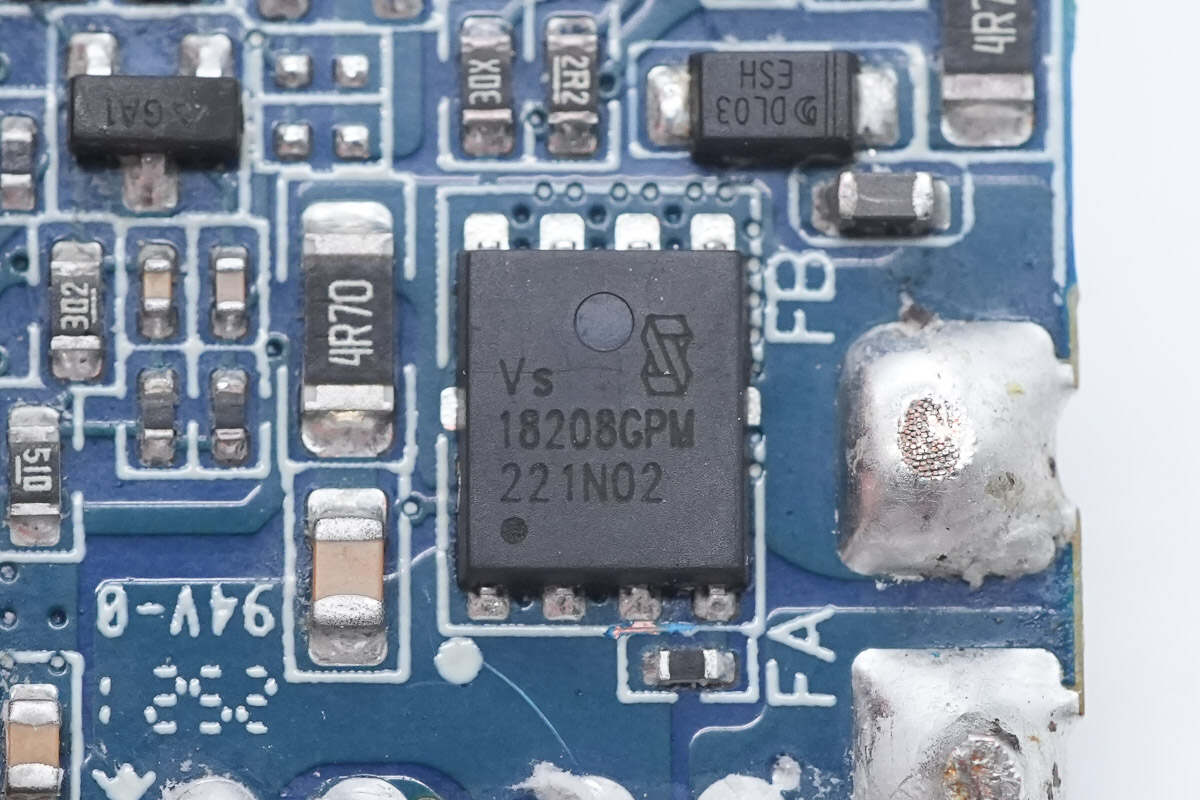
The synchronous rectifier is from Vergiga, model VS18208GPM. It is an N MOS rated for 100 V with an on-resistance of 3.8 mΩ, and comes in a PDFN5×6 package.
Here is the information about Vergiga VS18208GPM.
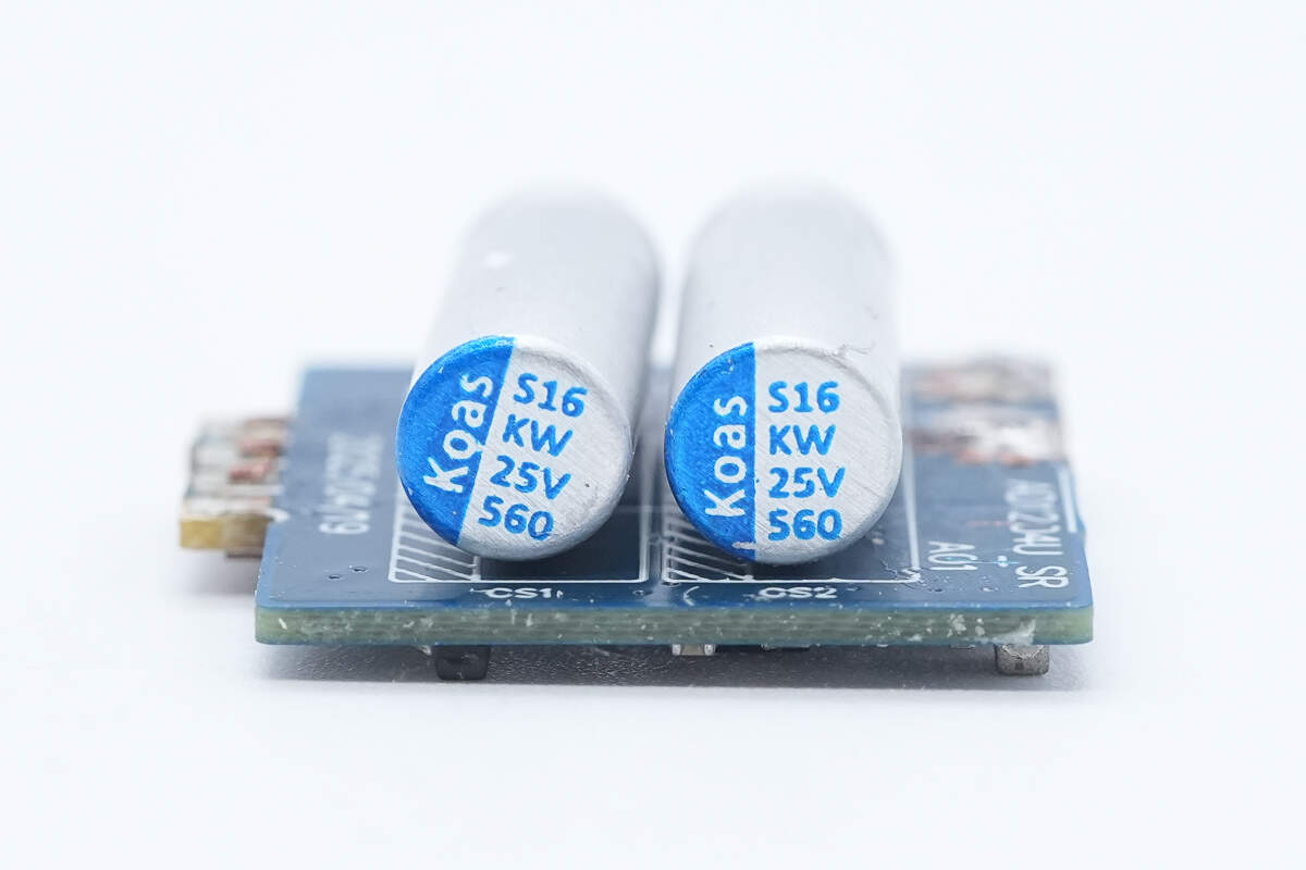
The two solid capacitors for output filtering are from Koshin, each rated at 25 V and 560 μF.
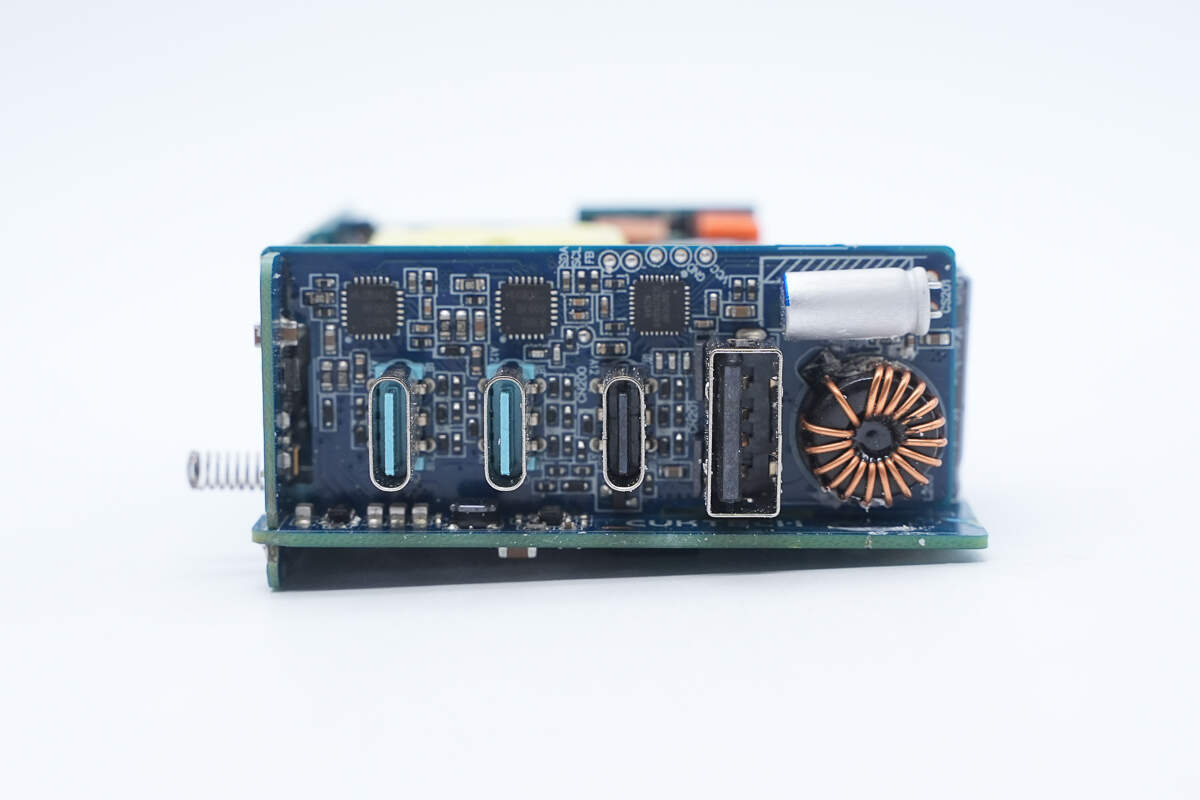
The USB sockets are soldered onto another small PCB.
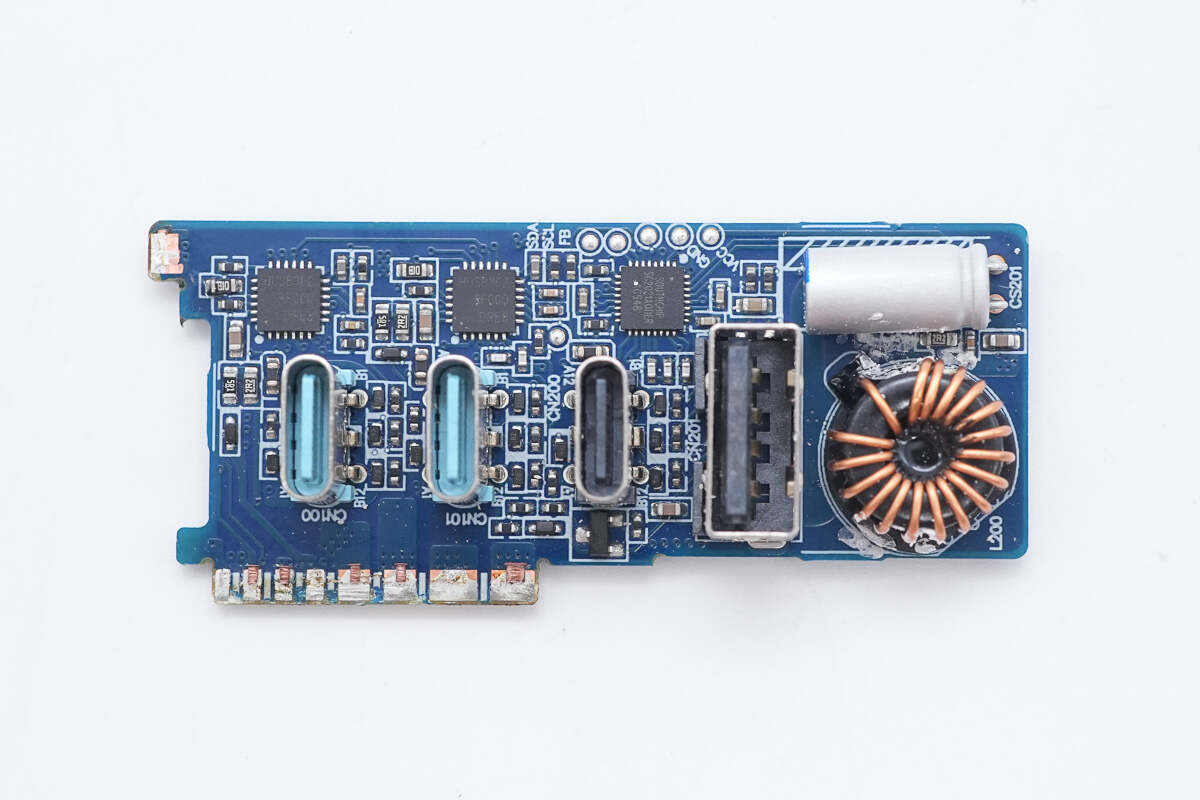
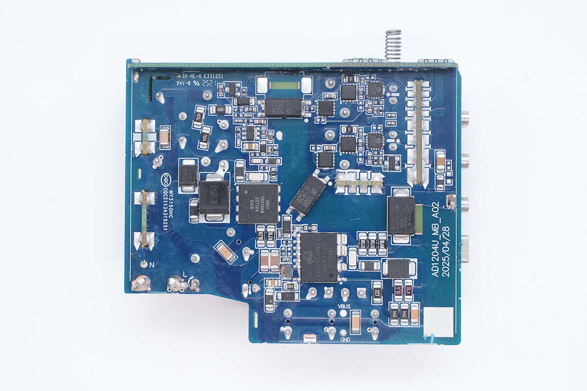
After removing the small PCB, the front side reveals protocol chips for the four USB ports, as well as the magnetic buck inductor and solid capacitor for the third secondary step-down circuit.
The back side has synchronous buck converters and the output VBUS MOSFETs for the four ports.
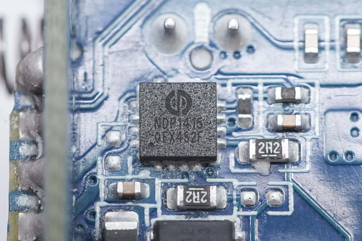
The synchronous buck controller used for the secondary step-down output of the USB-C1 port is from Deep-pool, model NDP1415. It is a 40 V-rated synchronous buck converter supporting input voltages up to 38 V. The device features constant voltage and constant current control, built-in line loss compensation, adjustable output voltage and switching frequency, burst mode support, integrated loop compensation, and soft-start functionality. It comes in a QFN-16 package.
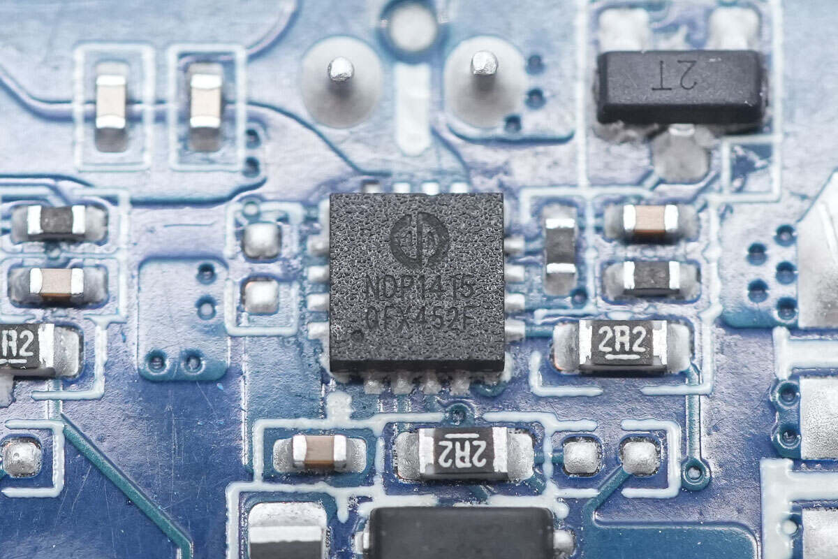
The secondary step-down output solution for the USB-C2 port also uses the Deep-pool NDP1415.
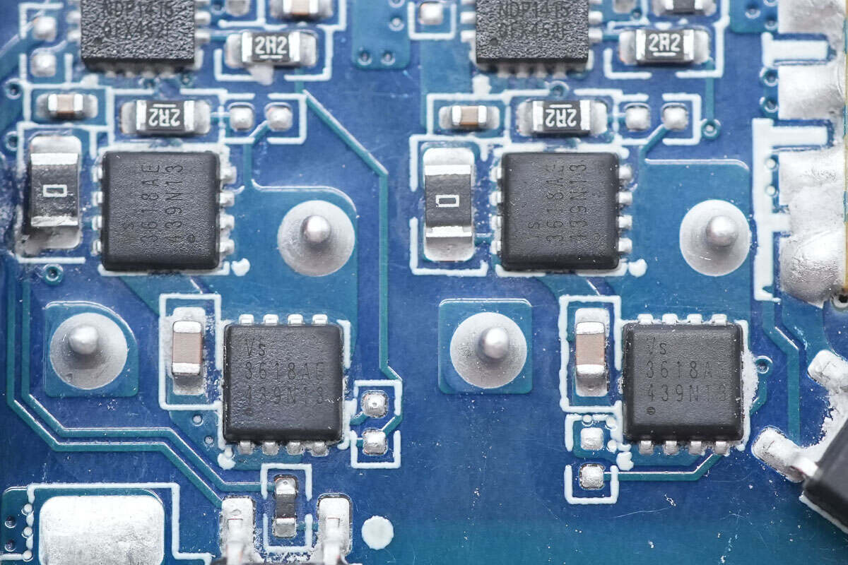
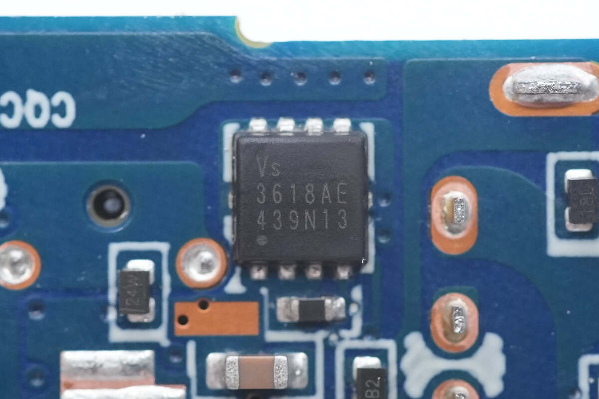
Each synchronous buck controller is paired with two synchronous buck MOSFETs, all of which are Vergiga VS3618AE. This is a 30 V-rated N-channel MOSFET with an on-resistance of 6.4 mΩ, housed in a PDFN3333 package.
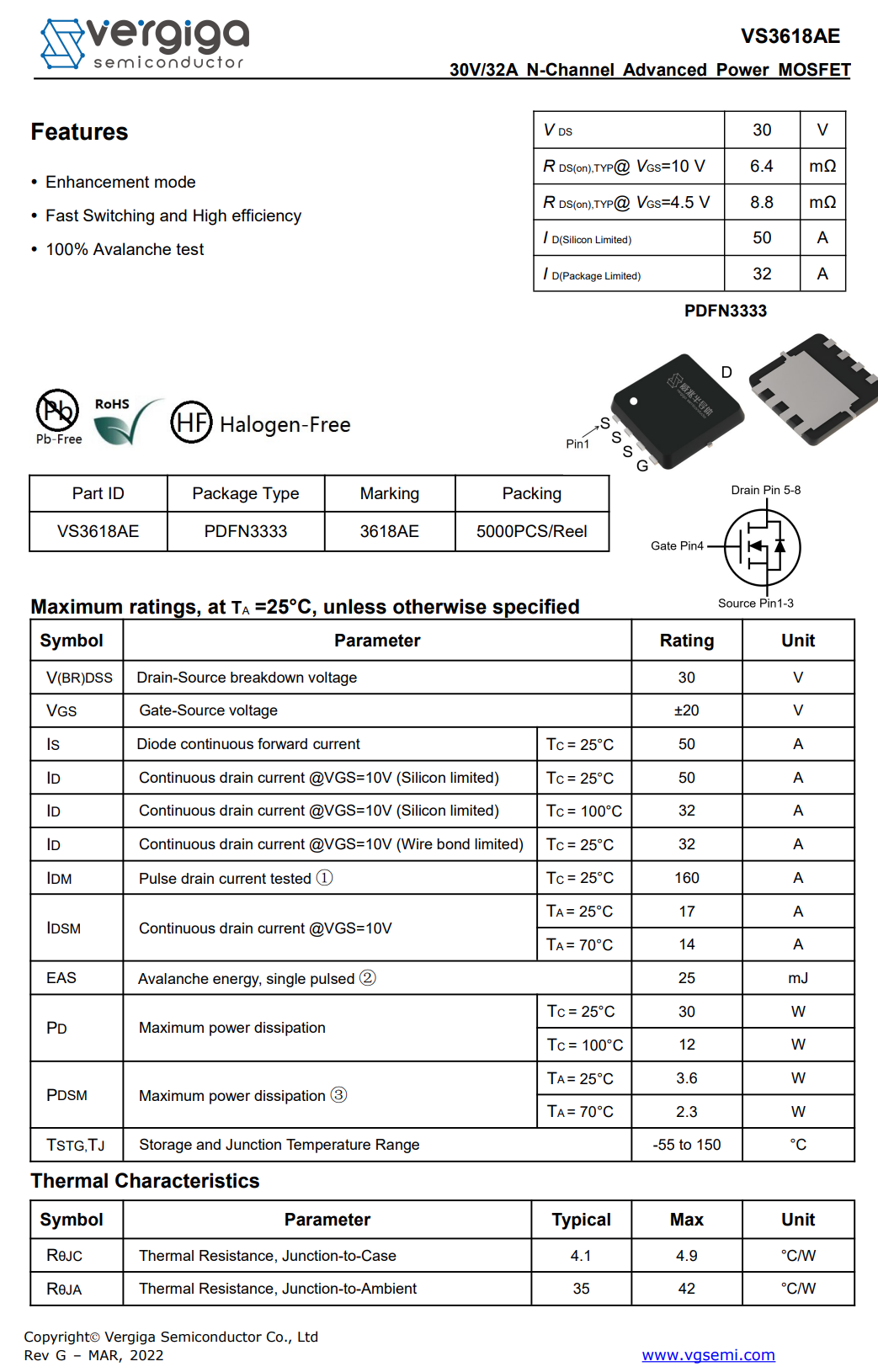
Here is the information about Vergiga VS3618AE.
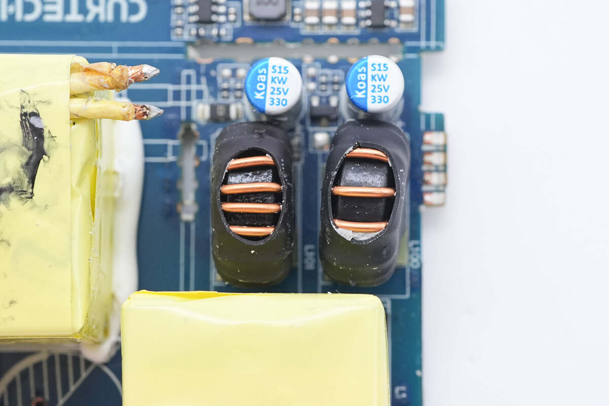
The two magnetic buck inductors are insulated with heat-shrinkable tubing.
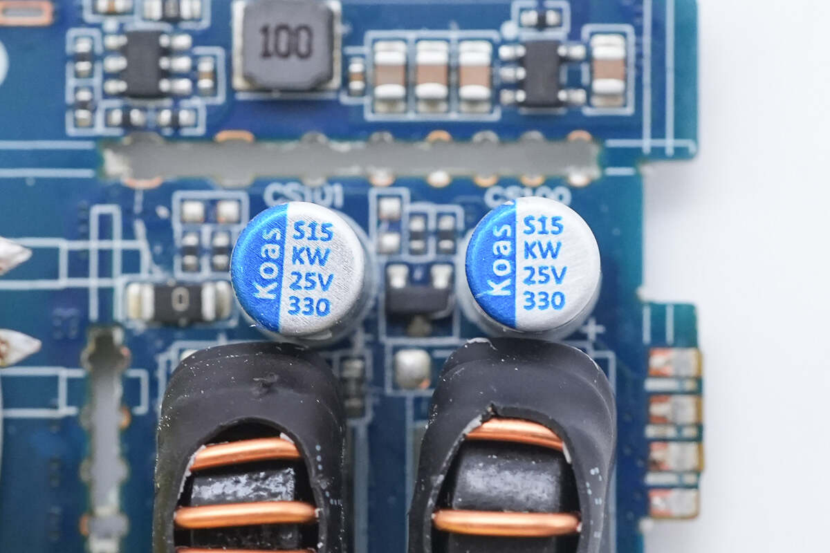
The solid capacitors used in the buck output stage are also from Koshin, each rated at 25 V and 330 μF.
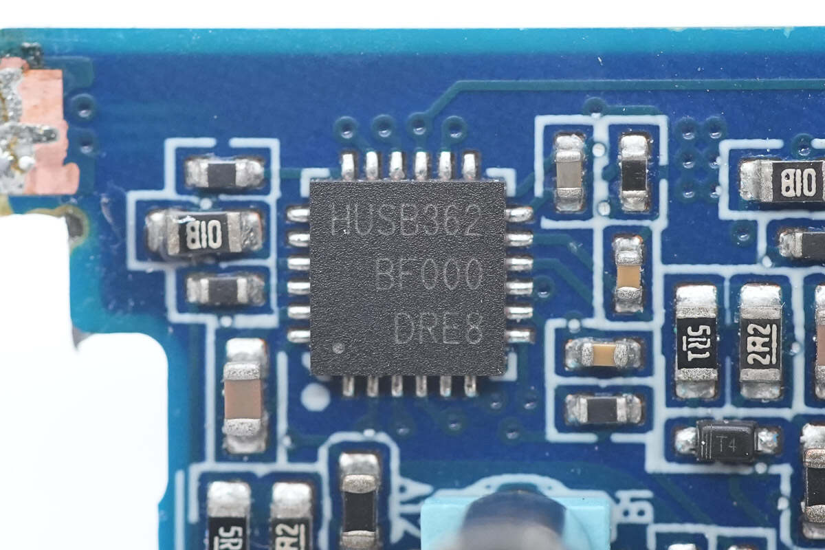
The protocol chip for the USB-C1 port is the HUSB362 from Hynetek. It is a high-performance PD protocol chip that supports USB PD 3.1 EPR and integrates a 32-bit RISC-V MCU. It features 32 KB of MTP memory and supports multiple programmable power data objects (PDOs), including PPS PDO and EPR PDO, all fully compliant with the USB PD 3.1 V1.7 specification. The HUSB362 has passed USB-IF PD 3.1 compliance testing, with an EPR TID of 9692.
The HUSB362 also implements a programmable DPDM PHY, with the D+ and D– pins configurable to support legacy charging protocols such as QC2.0, QC3.0, AFC, FCP, and Divider 3, ensuring broad compatibility with legacy devices.
Additionally, it integrates an N-MOS driver to control the conduction between VIN and VBUS, protecting the device connected to the Type-C port. The high voltage tolerance and protection on the CC1, CC2, D+, and D– pins enhance overall system reliability. The HUSB362 is also designed with comprehensive protection features for LPS (Limited Power Source) compliance.
The HUSB362 integrates high-quality constant voltage (CV) and constant current (CC) control loops, as well as a feedback (FB) voltage regulation mode, making it suitable for both AC-DC and DC-DC applications. Its dual-loop control architecture enables simplified peripheral component design, improving space efficiency and reducing design complexity while also lowering the overall BOM cost.
The USB-C2 port also uses the Hynetek HUSB362 as its protocol chip.
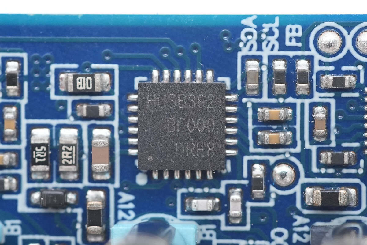
The output VBUS MOSFETs for both the USB-C1 and USB-C2 ports are AOS CQY7534N. These are 30 V NMOSs with an on-resistance of 4.8 mΩ, housed in a DFN3×3EP package.
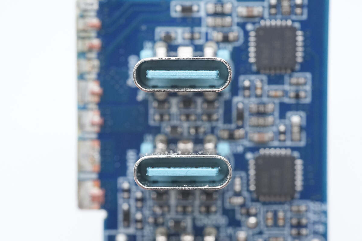
The USB-C1 and USB-C2 sockets use the same blue plastic sheet.
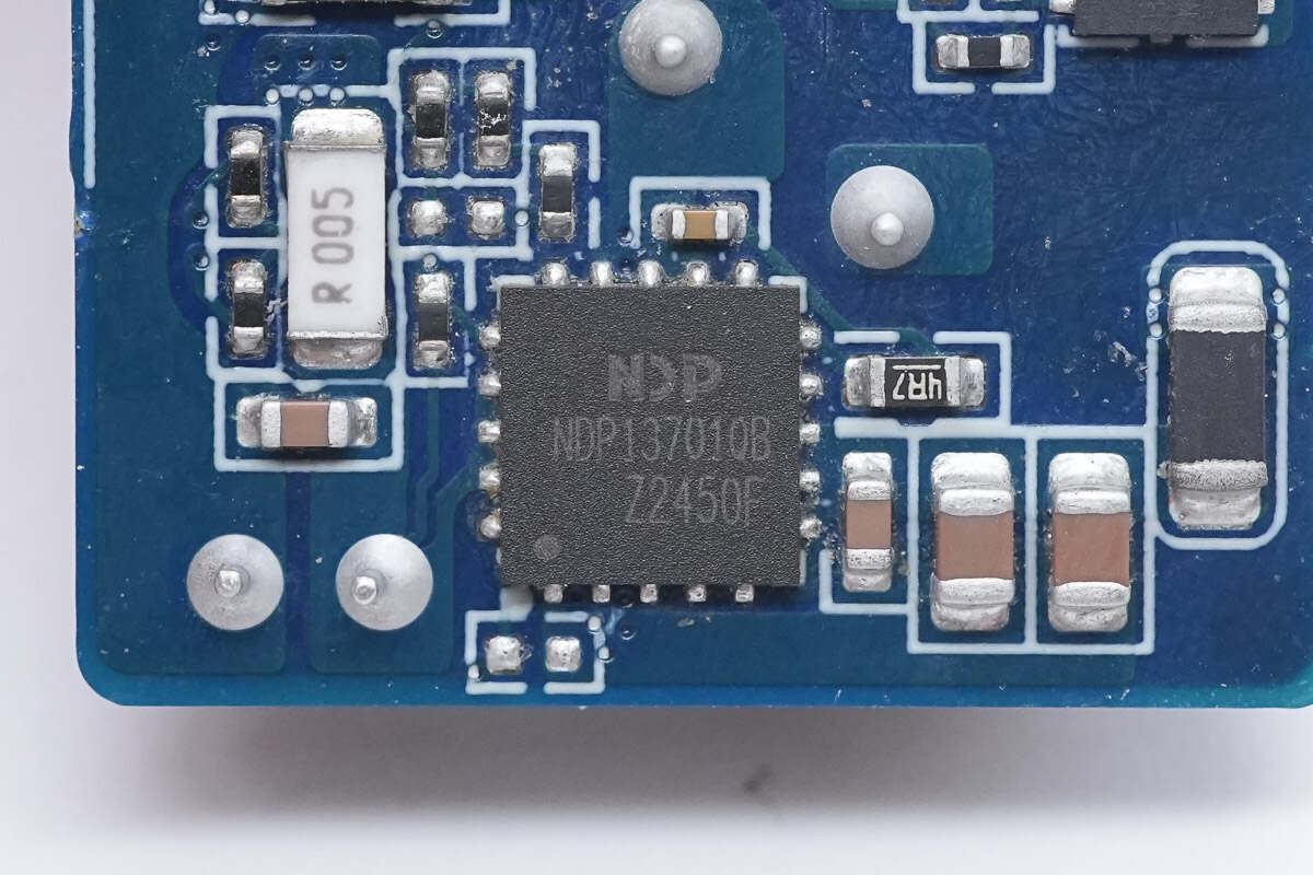
The synchronous buck converter used for the secondary step-down output of the other two ports is from Deep-pool, model NDP13701QB. It supports an input voltage range of 7–30 V and provides up to 7 A output current. The chip has integrated MOSFETs and comes in a QFN5×5 package.
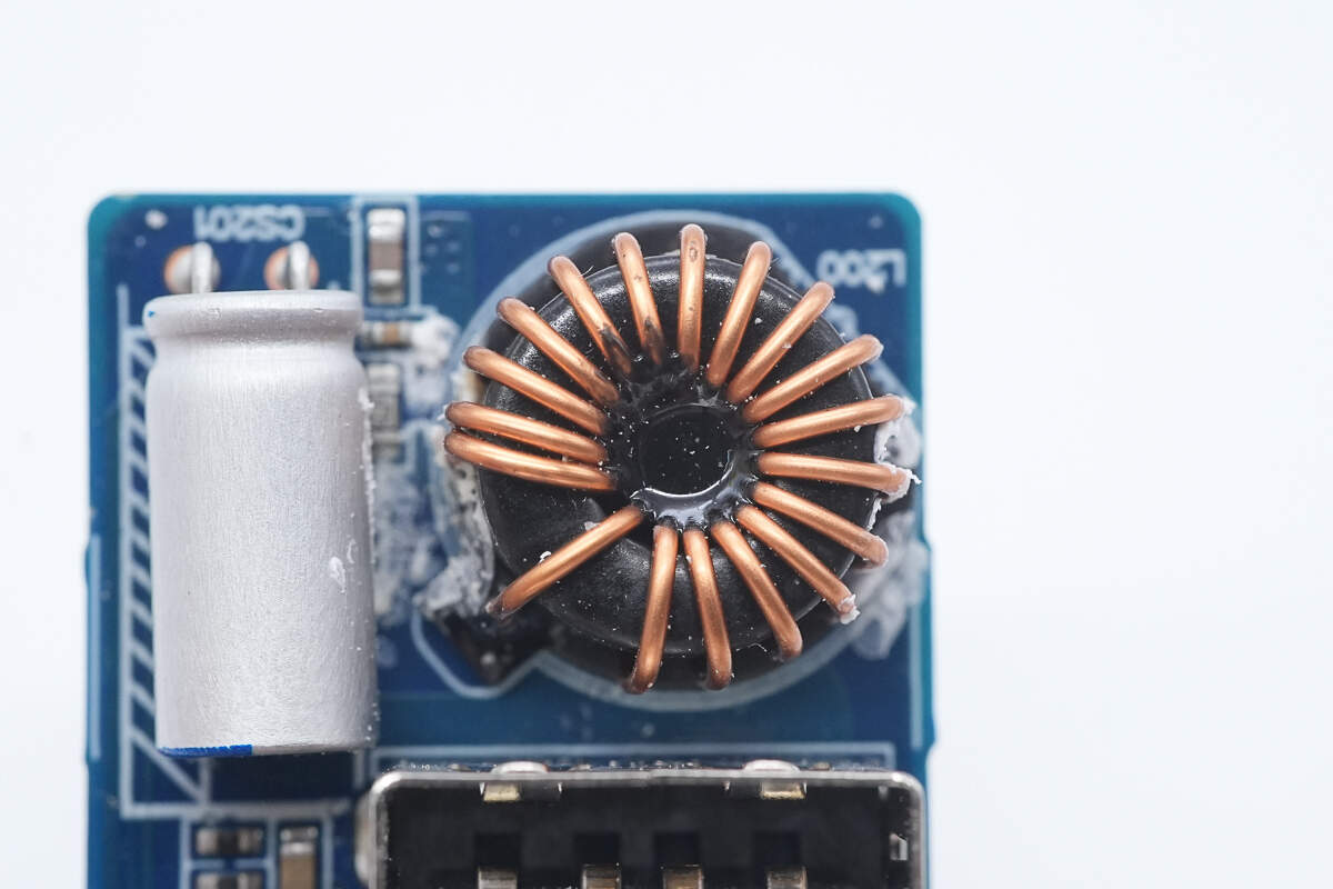
Close-up of the accompanying magnetic buck inductor.
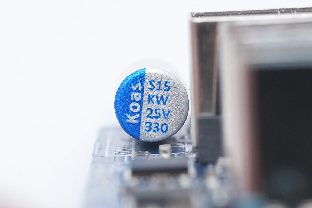
The secondary solid capacitor is from Koshin. 25V 330μF.
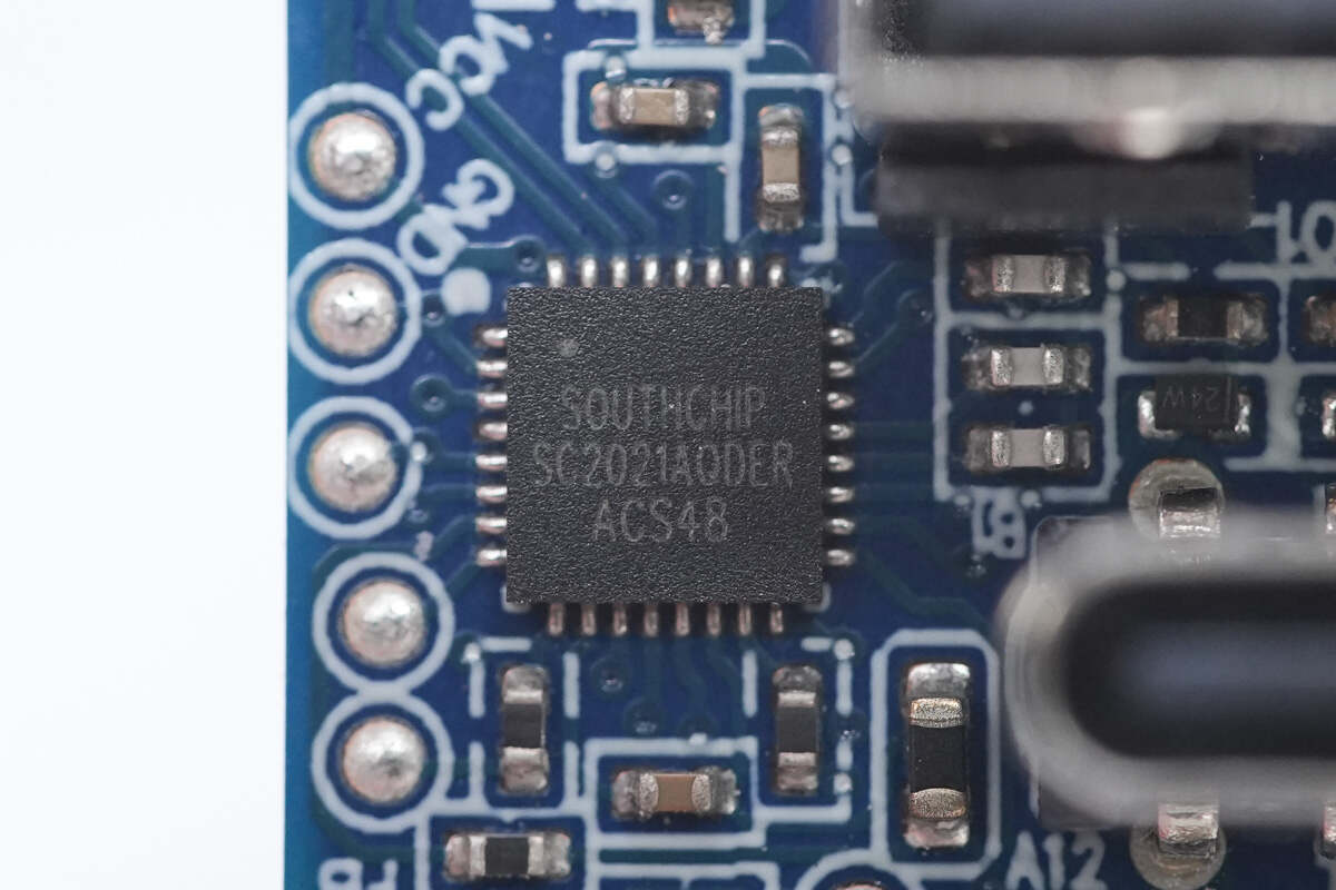
The protocol chip for the USB-C3 and USB-A ports is the SouthChip SC2021A, a highly integrated Type-C/PD and DPDM fast-charging controller. It complies with the latest Type-C and PD 3.0 standards and has passed USB PD 3.1 compliance testing. The chip supports proprietary high-voltage fast charging protocols and features one USB-C interface along with two DPDM interfaces, enabling dual-port fast charging with one USB-A and one USB-C port. It is packaged in a QFN32.
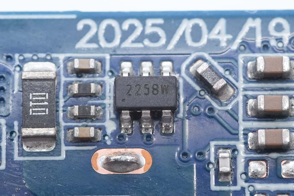
Close-up of a chip marked with 2258W.
The output VBUS MOSFET for the USB-C3 port is the Vergiga VS3618AE.
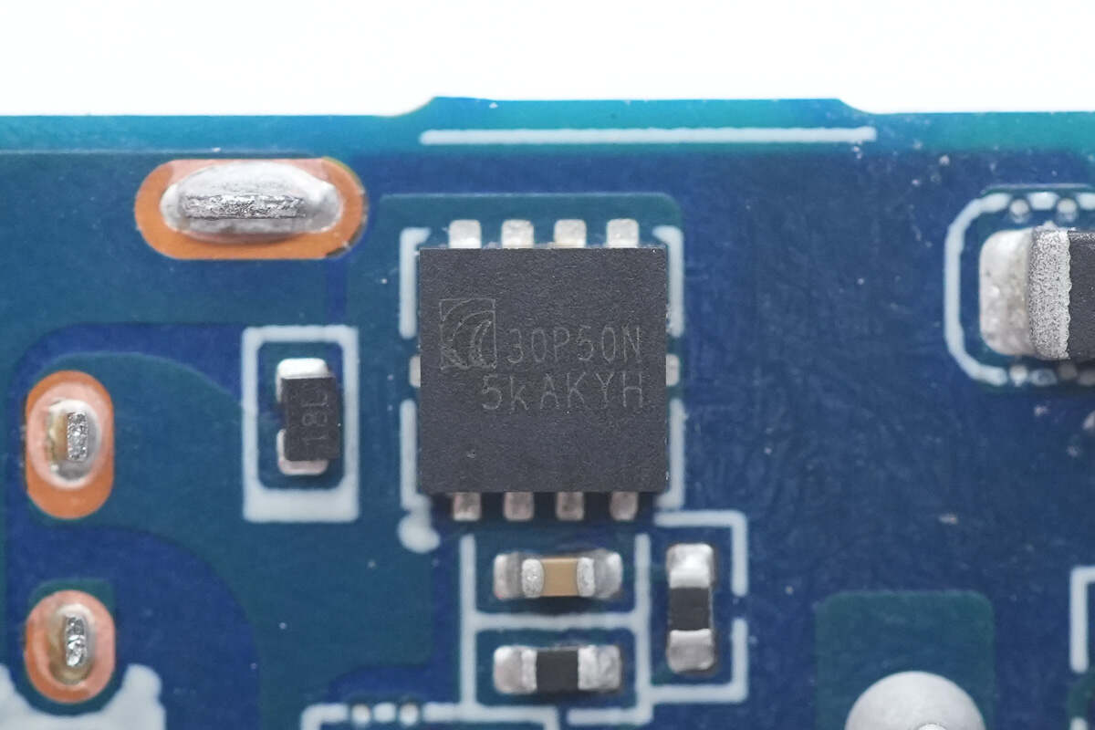
The output VBUS MOSFET for the USB-A port is marked with 30P50N.
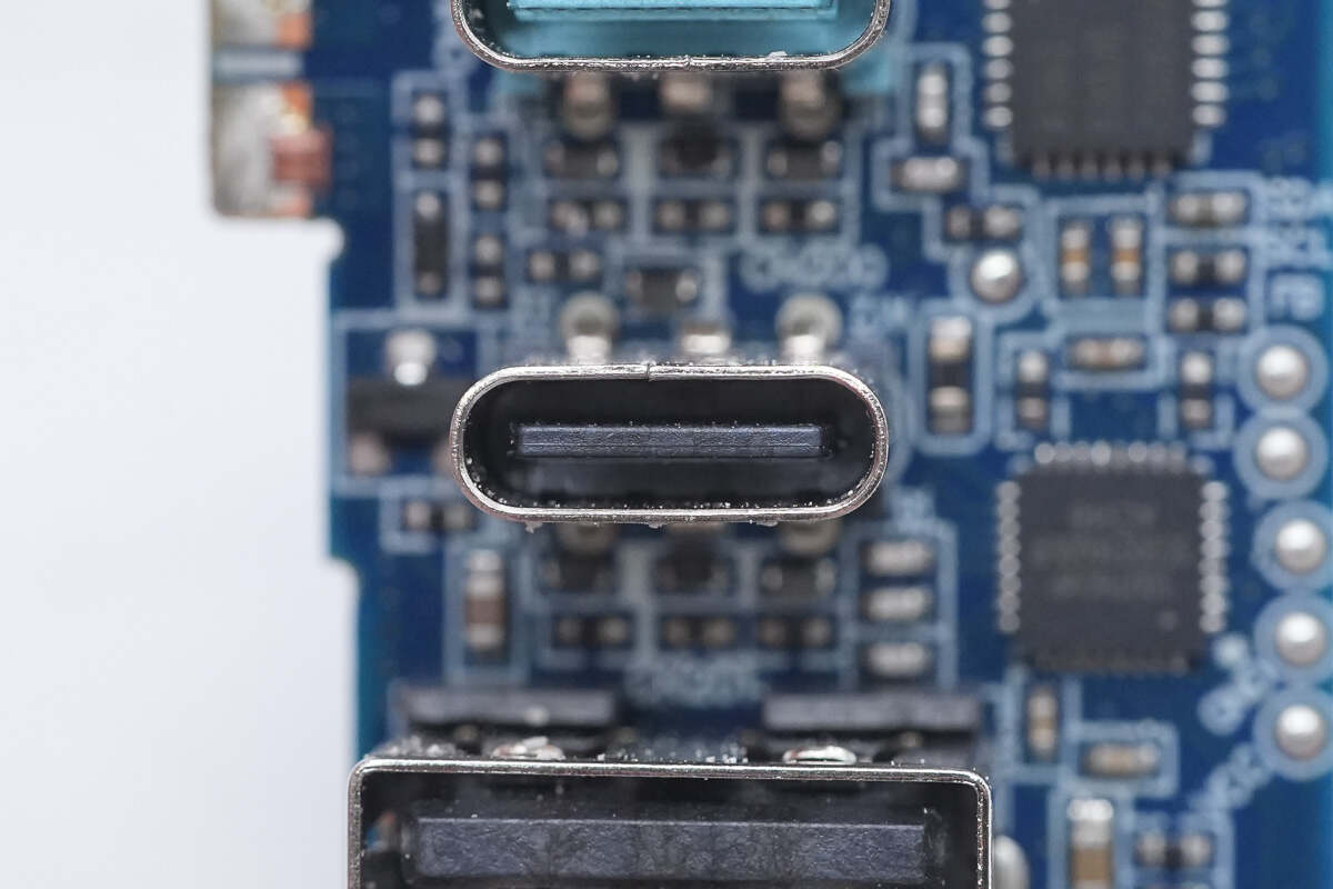
Close-up of the USB-C3 socket.
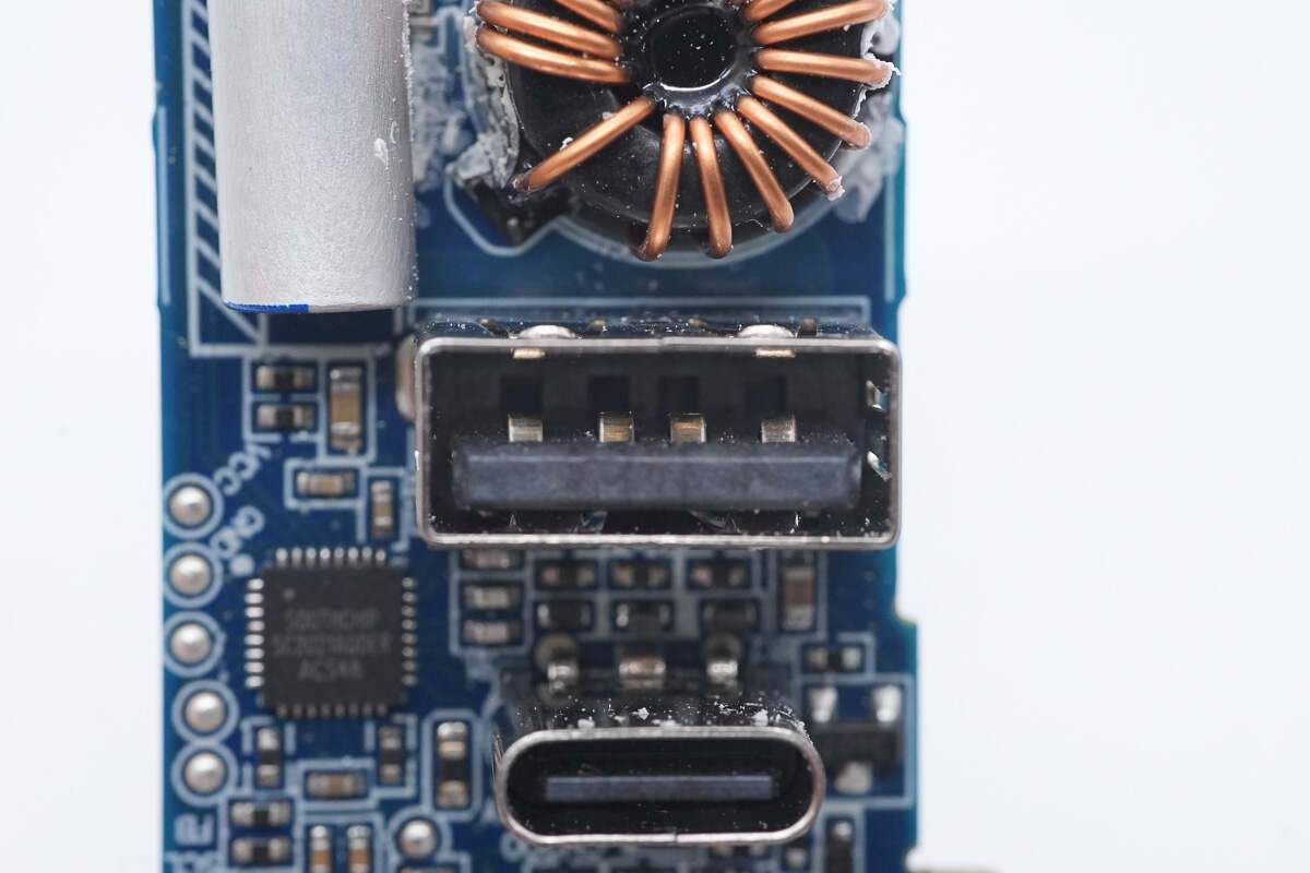
Close-up of the USB-A socket.
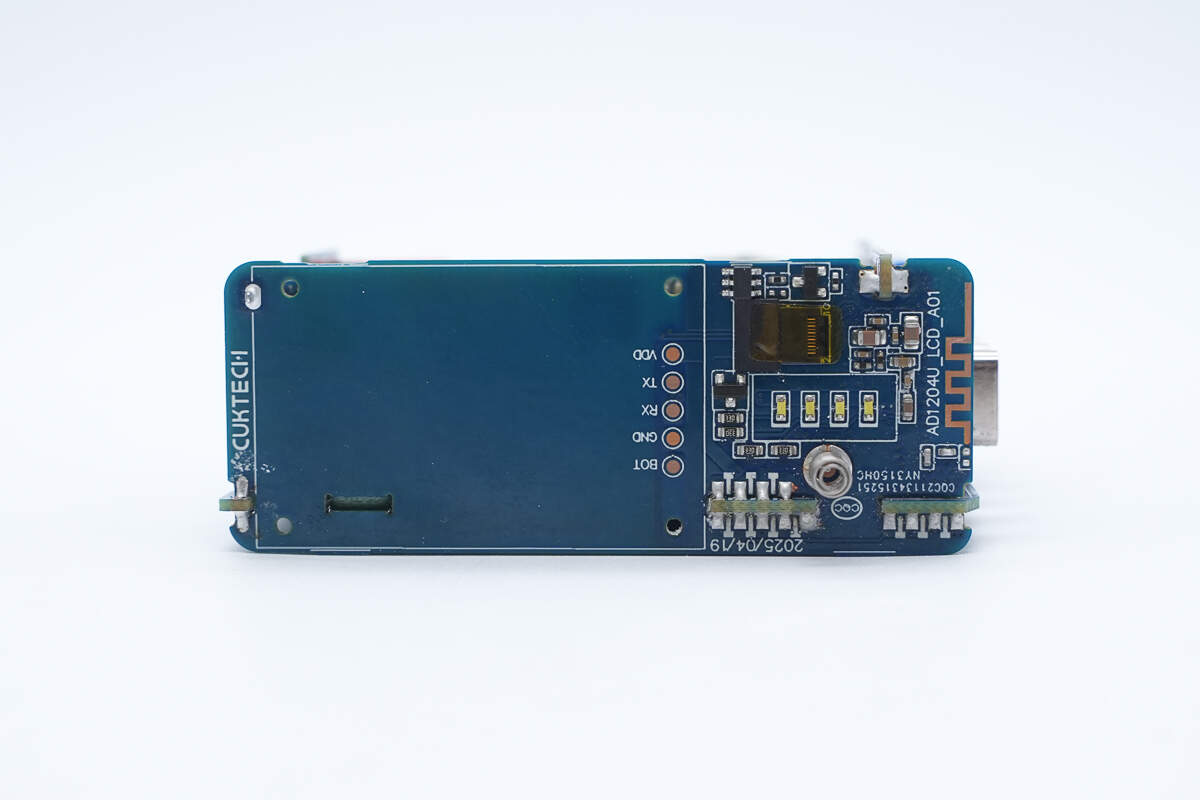
The front side of the third small PCB features LED indicators, and the ribbon cable connector is wrapped with high-temperature insulating tape.
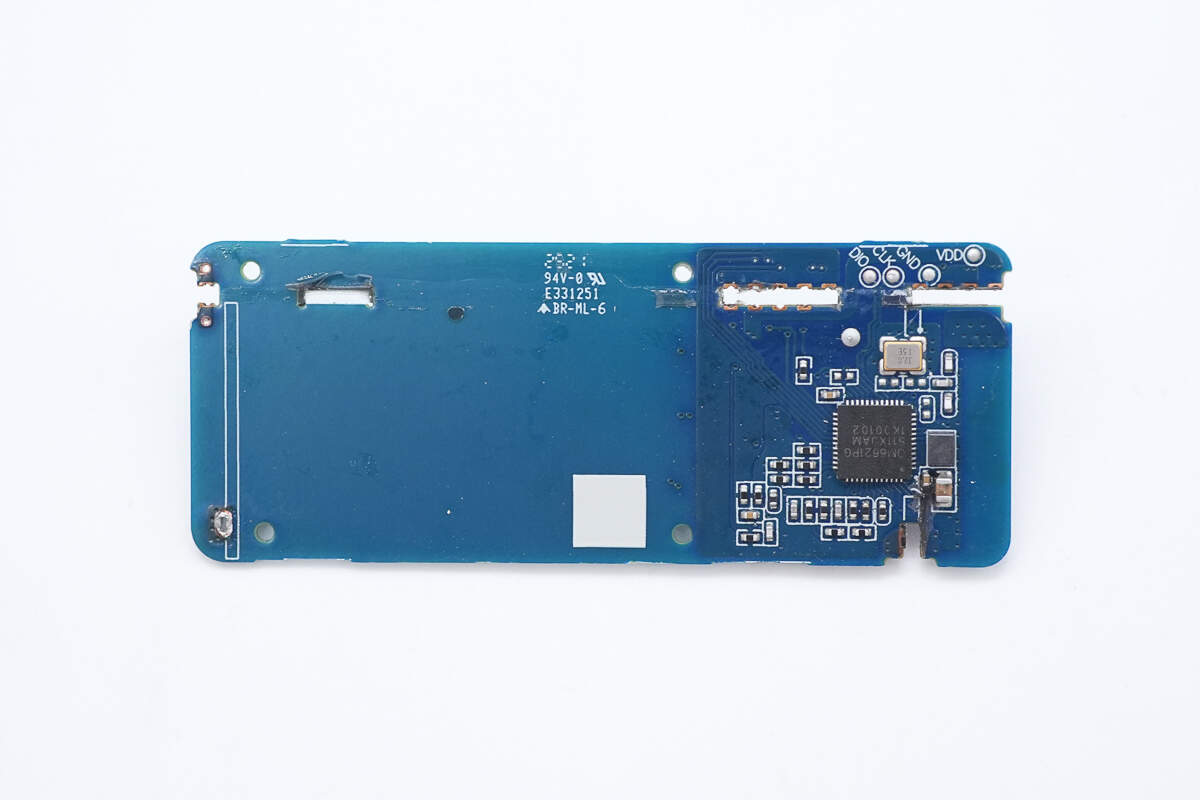
The back side houses the MCU and an external clock crystal oscillator.
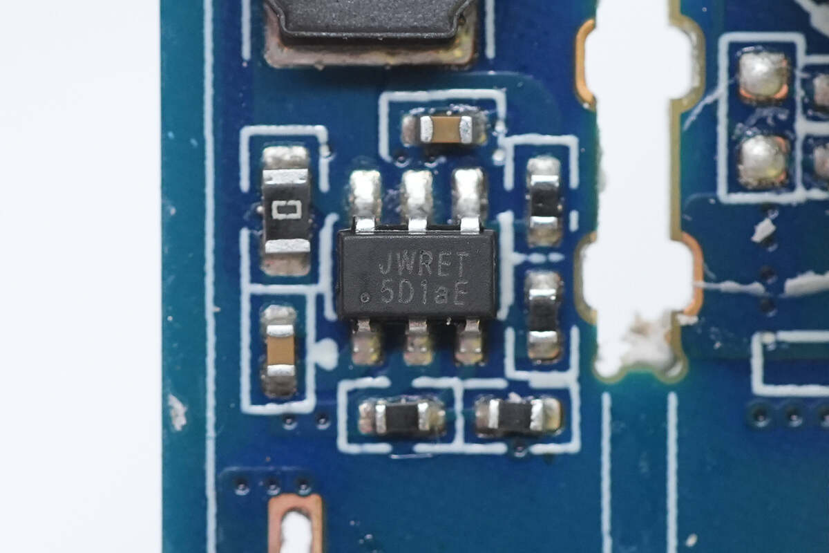
The synchronous buck converter used to power the MCU is from Joulwatt, marked as JWRE, with the model number JW5018XSOTB. It supports an input voltage range of 4.5V to 42V and can deliver a continuous output current of 600mA through two internally integrated NMOSs. The built-in synchronous power switches eliminate the need for an external Schottky diode, enabling high efficiency.
Here is the information about JOULWATT JW5018XSOTB.
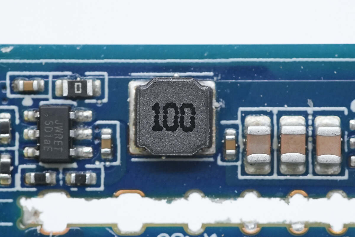
Close-up of the accompanying buck inductor.
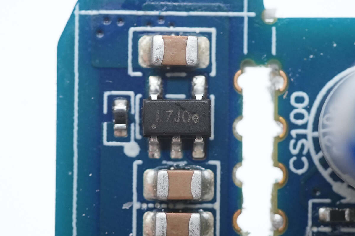
The regulator chip is from 3PEAK, marked with L7J, model TPL720F33. It supports an input voltage of up to 6V and provides a 3.3V output voltage with a maximum output current of 400mA. The chip features current limiting and overcurrent protection and comes in a SOT23-5 package.
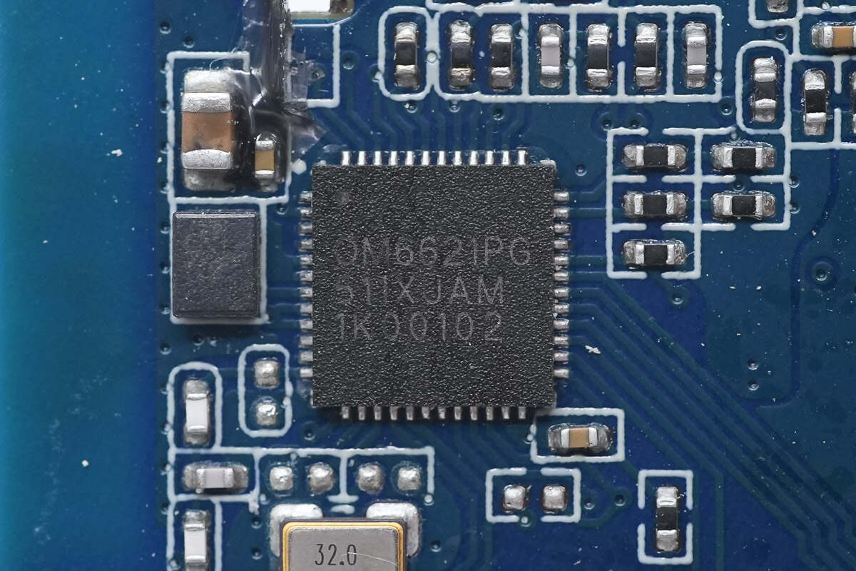
The Bluetooth SoC is from OnMicro, model OM6621Px. It is a power-optimized SoC solution designed for Bluetooth Low Energy (BLE) and proprietary 2.4GHz applications. The chip integrates a high-performance, low-power RF transceiver, Bluetooth baseband, and a wide range of peripheral interfaces. It also includes a built-in power management unit (PMU) for efficient power regulation. The device is packaged in a QFN48 package.
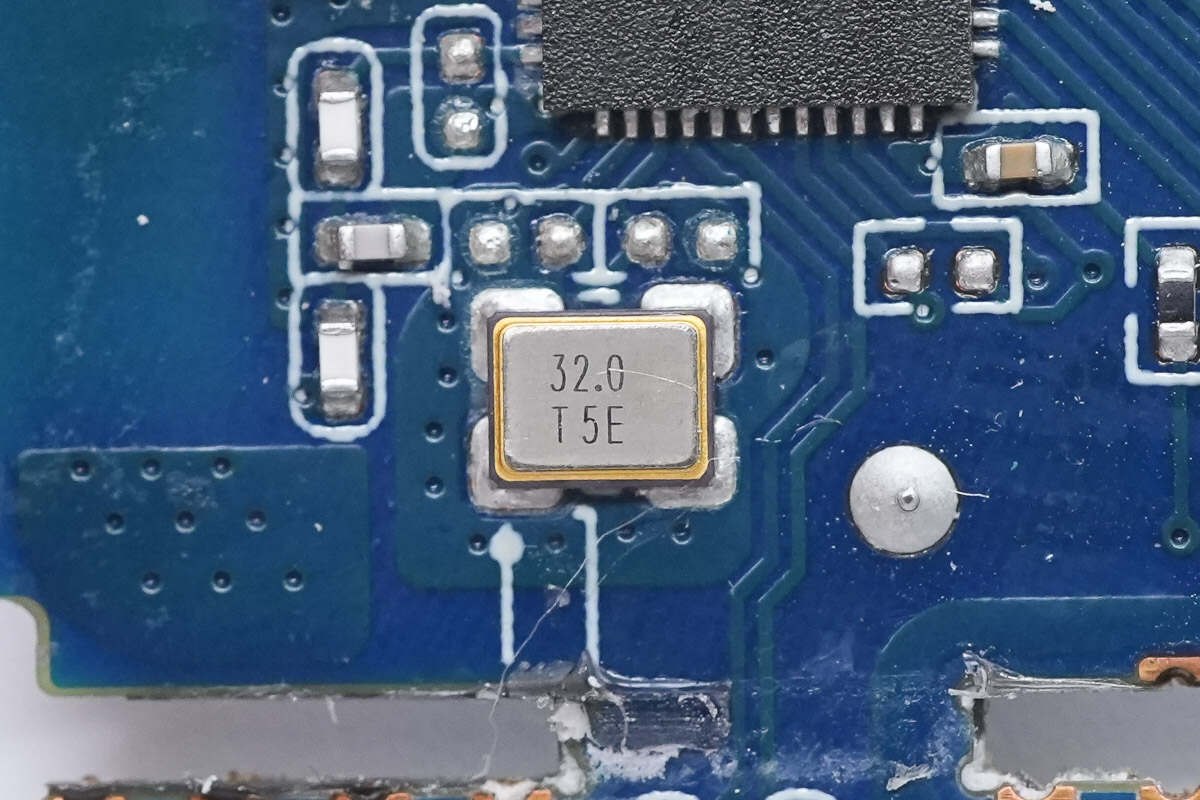
Close-up of the external 32.0 MHz crystal oscillator for the MCU.
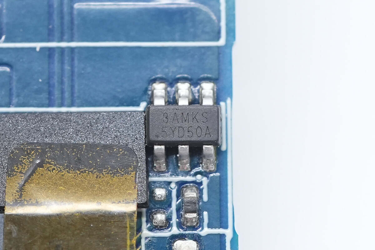
The touch chip is marked with 3AMKS and comes in a SOT23-6 package.
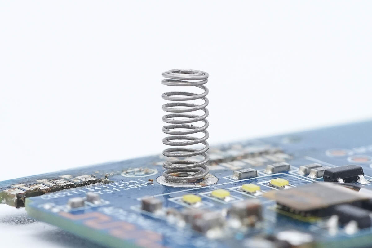
Close-up of the touch spring.
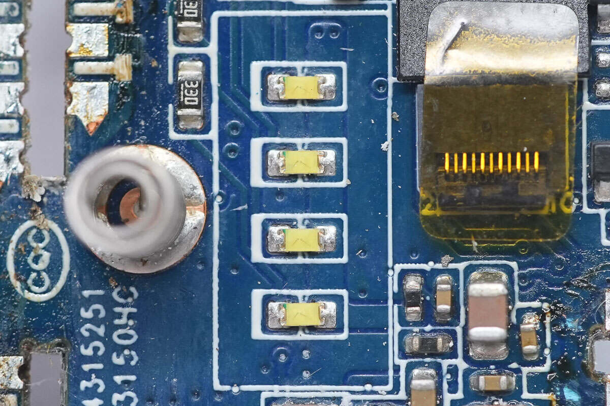
Close-up of the LED indicators.
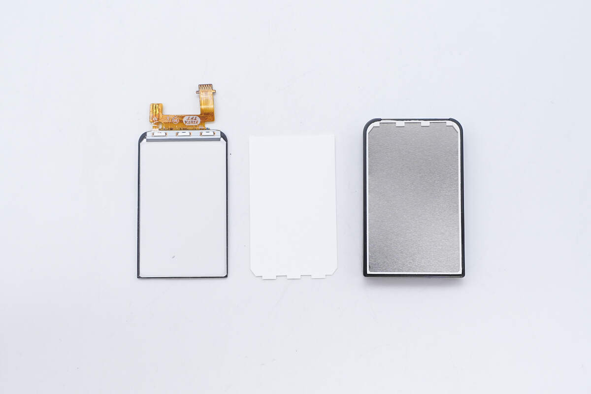
Overview of the disassembled screen.

Well, those are all components of the CUKTECH 10 GaN Charger Ultra.
Summary of ChargerLAB
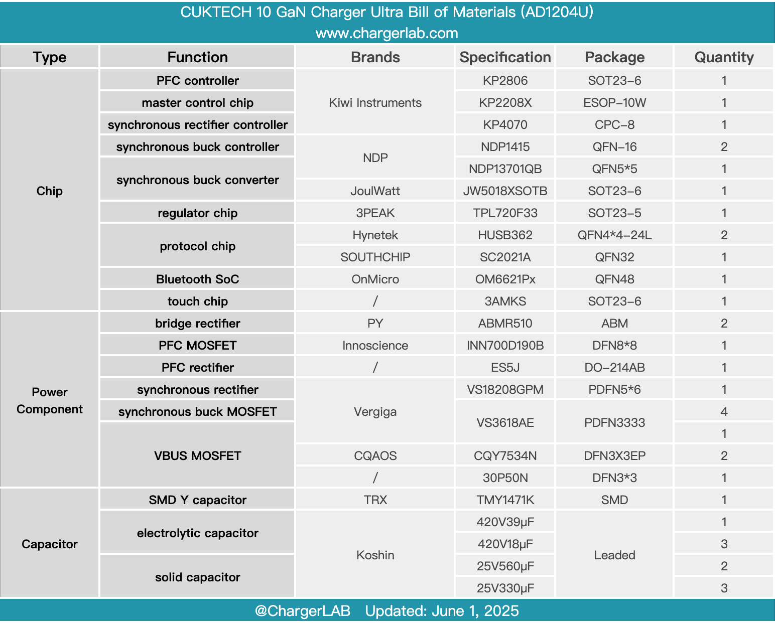
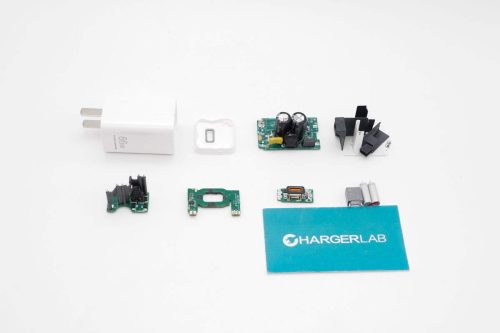
Here is the component list of the CUKTECH 10 GaN Charger Ultra for your convenience.
It features a stylish design with foldable prongs and is equipped with a feature-rich display. It can connect to the Xiaomi Home app to enable a variety of customizable functions. It includes three USB-C ports and one USB-A port, supporting protocols such as PD/PPS up to 100W, UFCS 44W, and Xiaomi's proprietary 120W fast charging. It also supports adaptive dynamic power distribution.
After taking it apart, we found that it is designed based on a PFC + QR flyback topology, featuring three independent secondary DC-DC buck outputs. It adopts a complete power solution from Kiwi Instruments, including the KP2806, KP2208X, and KP4070. The design is complemented by an Innoscience INN700D190B PFC MOSFET and a Vergiga VS18208GPM synchronous rectifier.
The USB ports utilize Deep-pool’s synchronous buck solution for secondary step-down conversion. Interface output is managed by the Hynetek HUSB362 and SouthChip SC2021A protocol chips. Bluetooth connectivity and display functions are handled by the OnMicro OM6621Px Bluetooth SoC. All filtering capacitors are supplied by Koshin.
In addition to the main PCB, several smaller PCBs are soldered onto it. The outer layer is covered with a copper heatsink, and both the front and back sides are filled with potting compound. Together with a proprietary algorithm and NTC hardware, this design ensures charging safety.
Related Articles:
1. Teardown of Lenovo thinkplus FLUXO 140W 20000mAh Power Bank (SLPB-20140)
2. Teardown of DJI 2600W 1024Wh Power 1000 V2 Portable Power Station
3. Teardown of HUAWEI 100W SuperCharge Car Charger (P0019)