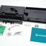
Introduction
This teardown features a BYD in-car pre-installed wireless charging module. It features a plastic panel with a single charging pad. The back is equipped with a metal casing and a built-in cooling fan, enhancing the performance of high-power wireless charging. The power input is located on the back and is labeled with an information tag. The maximum wireless charging power is 50W. Next, let’s take a closer look at its internal components and design.
Product Appearance

The metal backplate is secured with screws.

The front features a plastic housing.
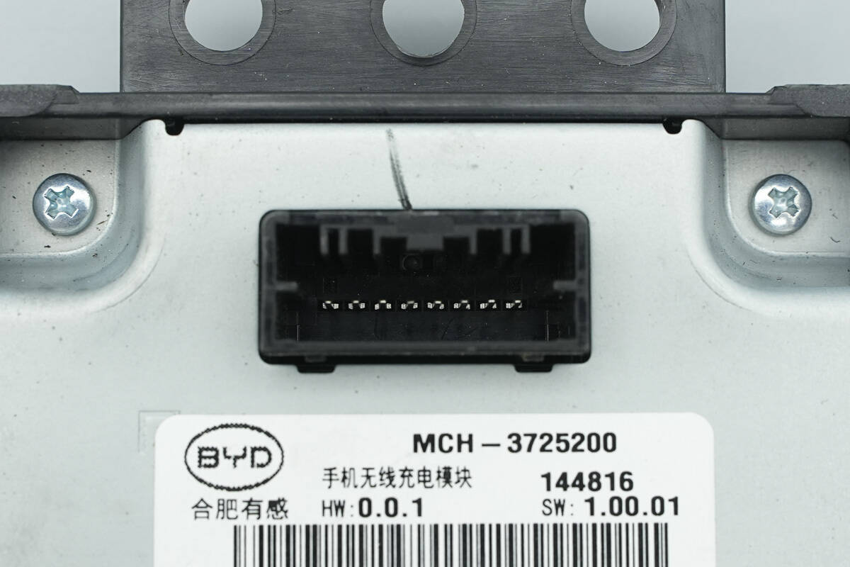
The power connection terminal is located at the top of the back cover.
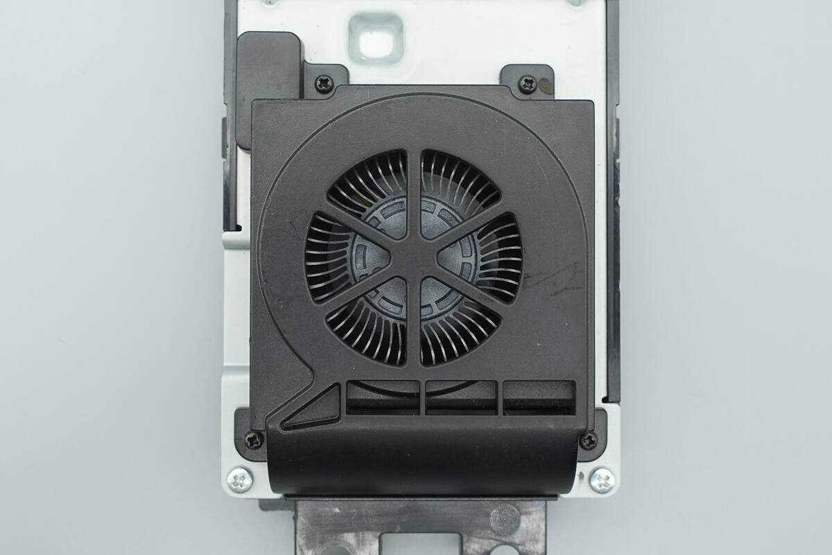
The cooling fan is located at the bottom.
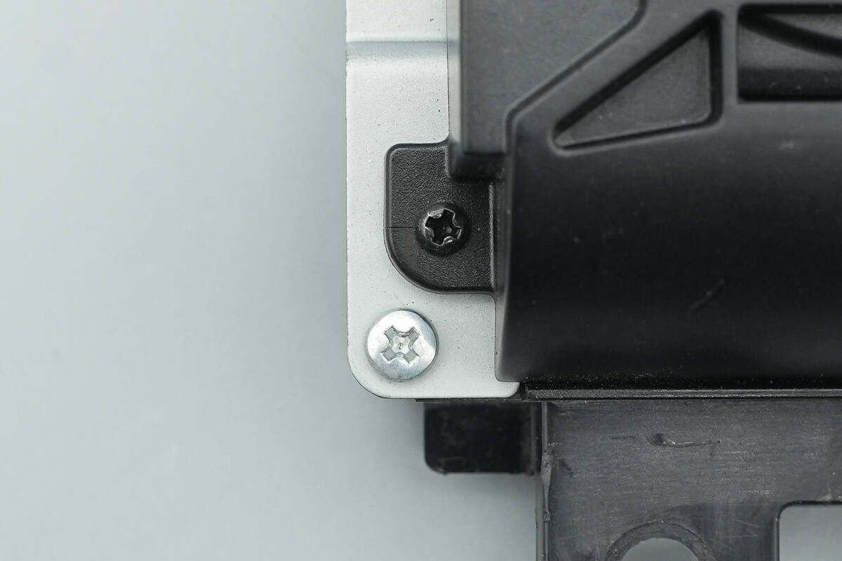
A close-up of the fastening screws.
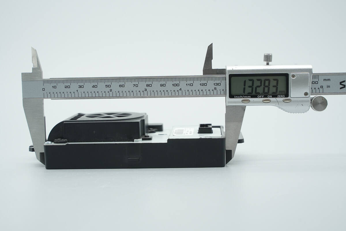
The length of the module is about 132.8 mm (5.23 inches).
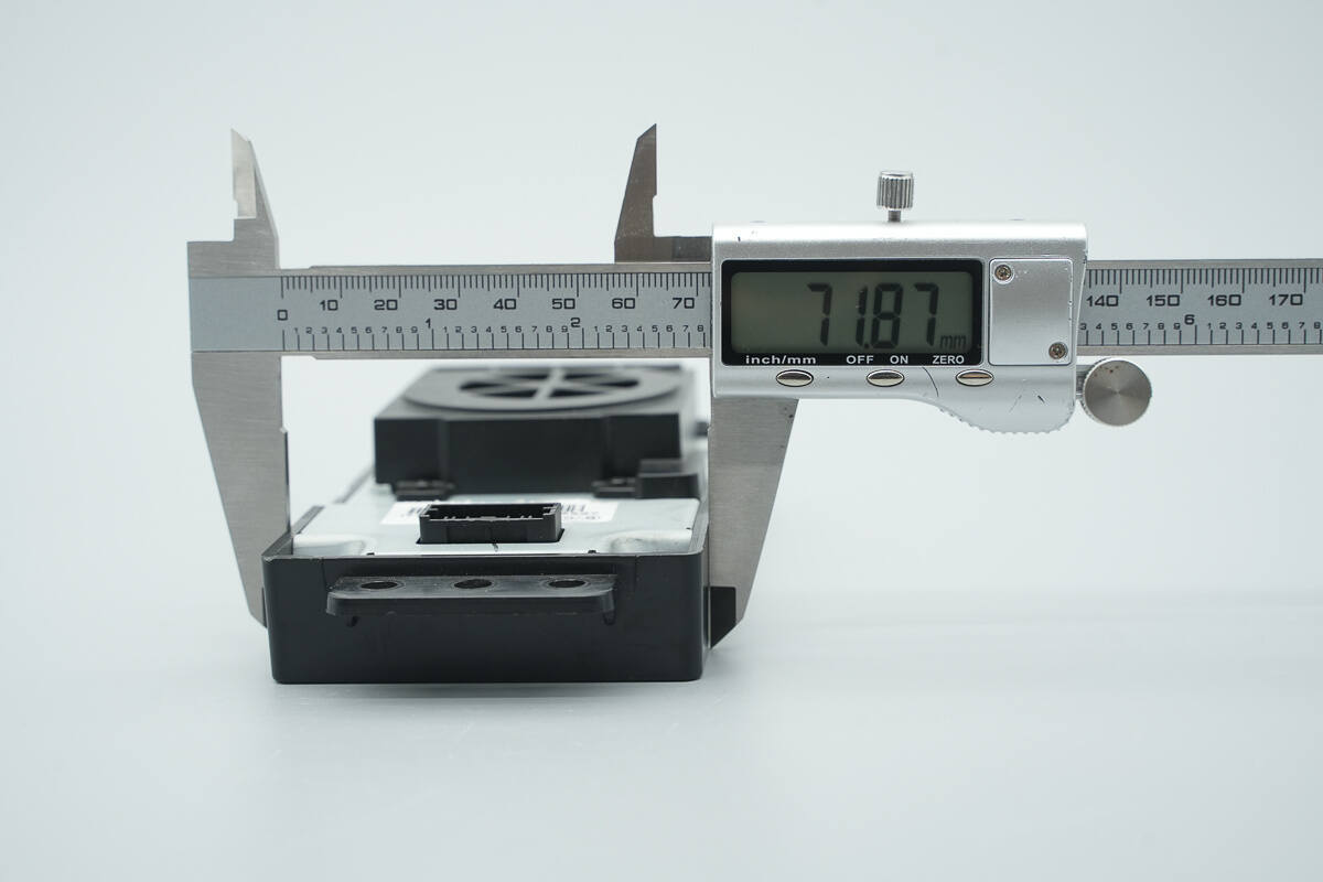
The width is about 71.9 mm (2.83 inches).
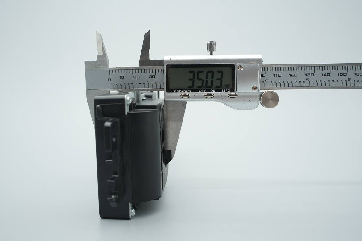
The thickness is about 35 mm (1.38 inches).
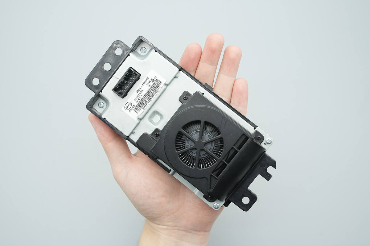
That's how big it is in the hand.
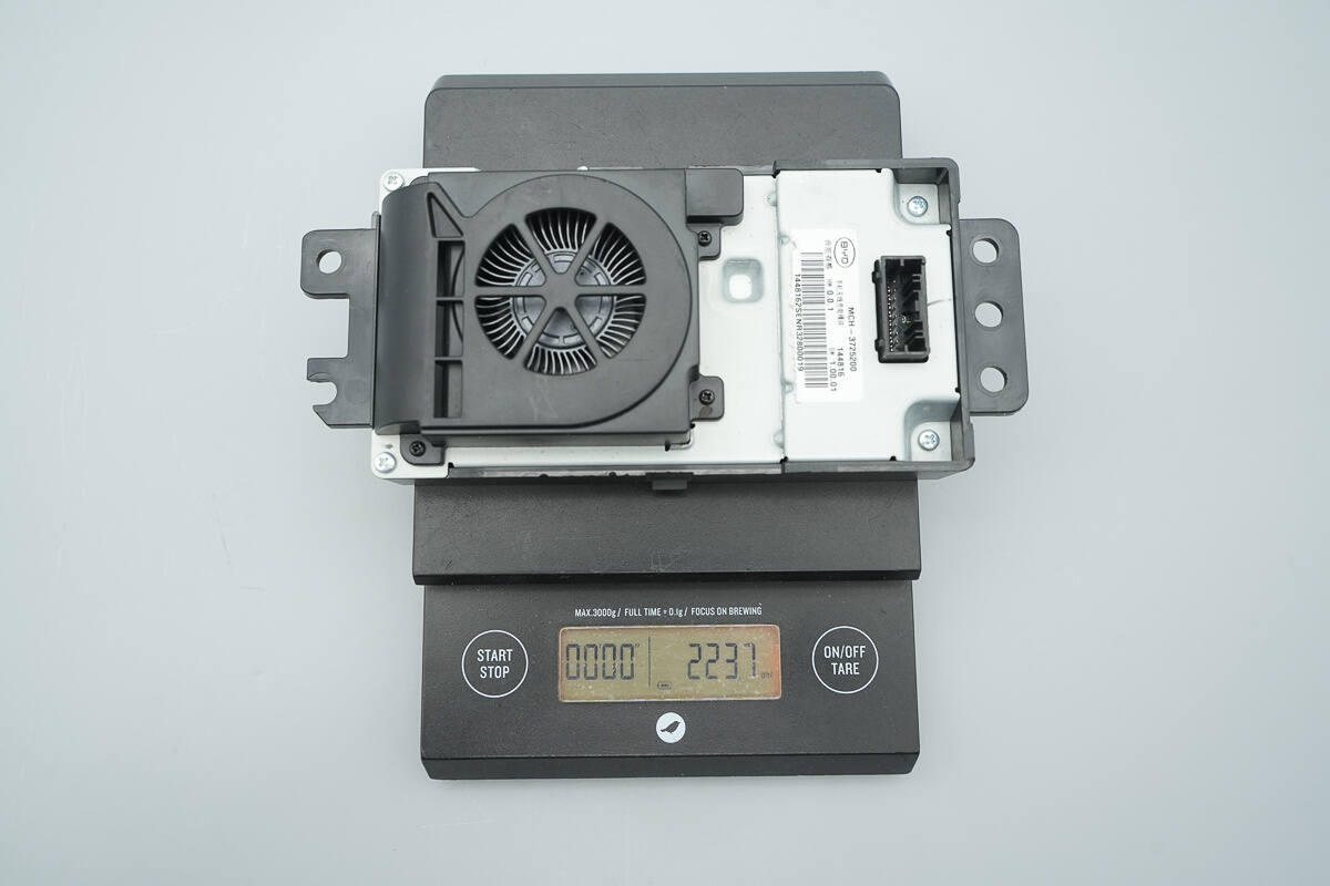
The weight is about 224 g (7.9 oz).
Teardown
Next, let's take it apart to see its internal components and structure.

Remove the screws and the back cover.

The fan is connected via a connector.
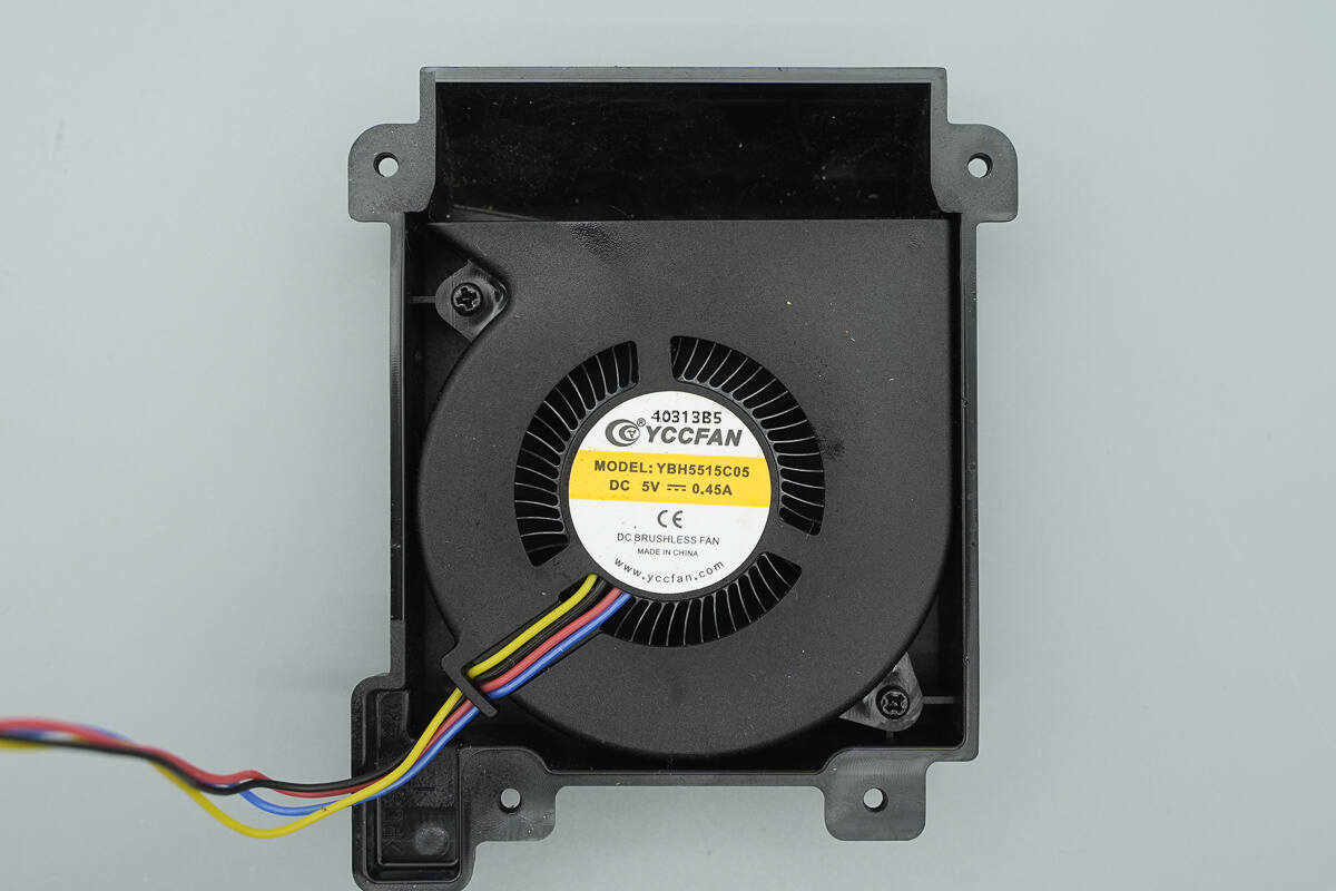
The fan is from YCCFAN, model YBH5515C05, with a specification of 5V 0.45A.
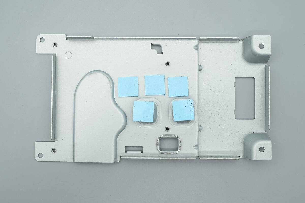
Inside the metal casing, there are thermal pads.
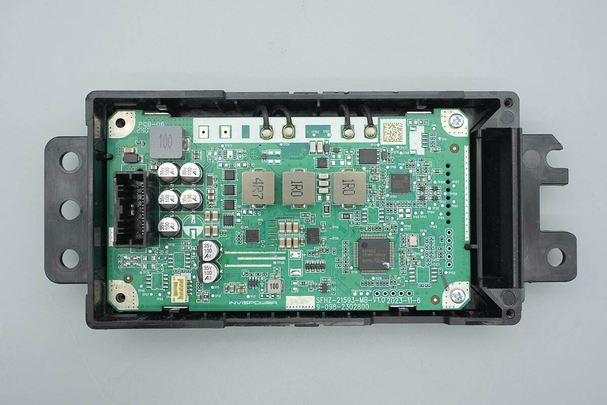
The PCBA module is secured inside the casing with screws.
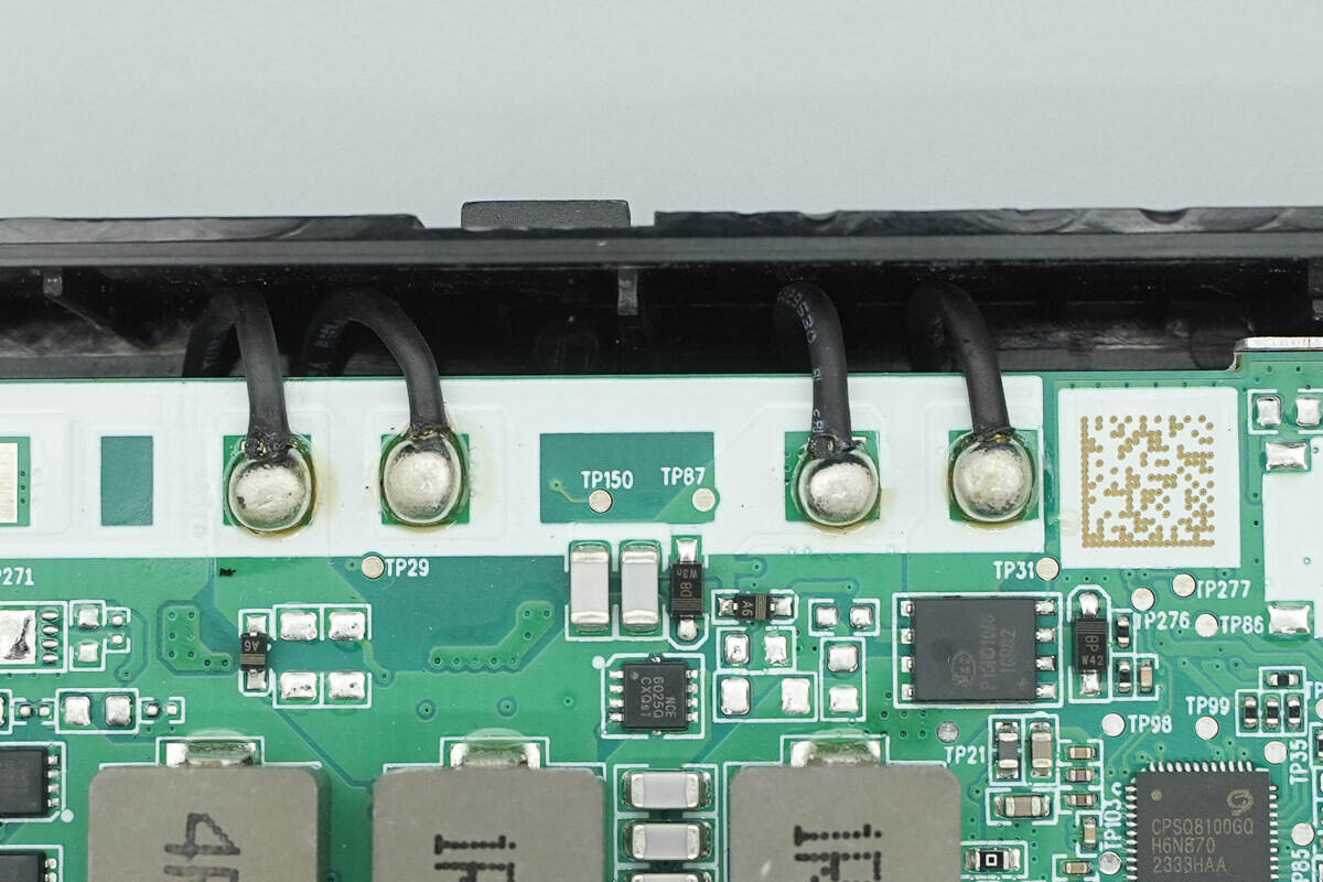
The charging coil is connected via soldering, with smooth and full solder joints.
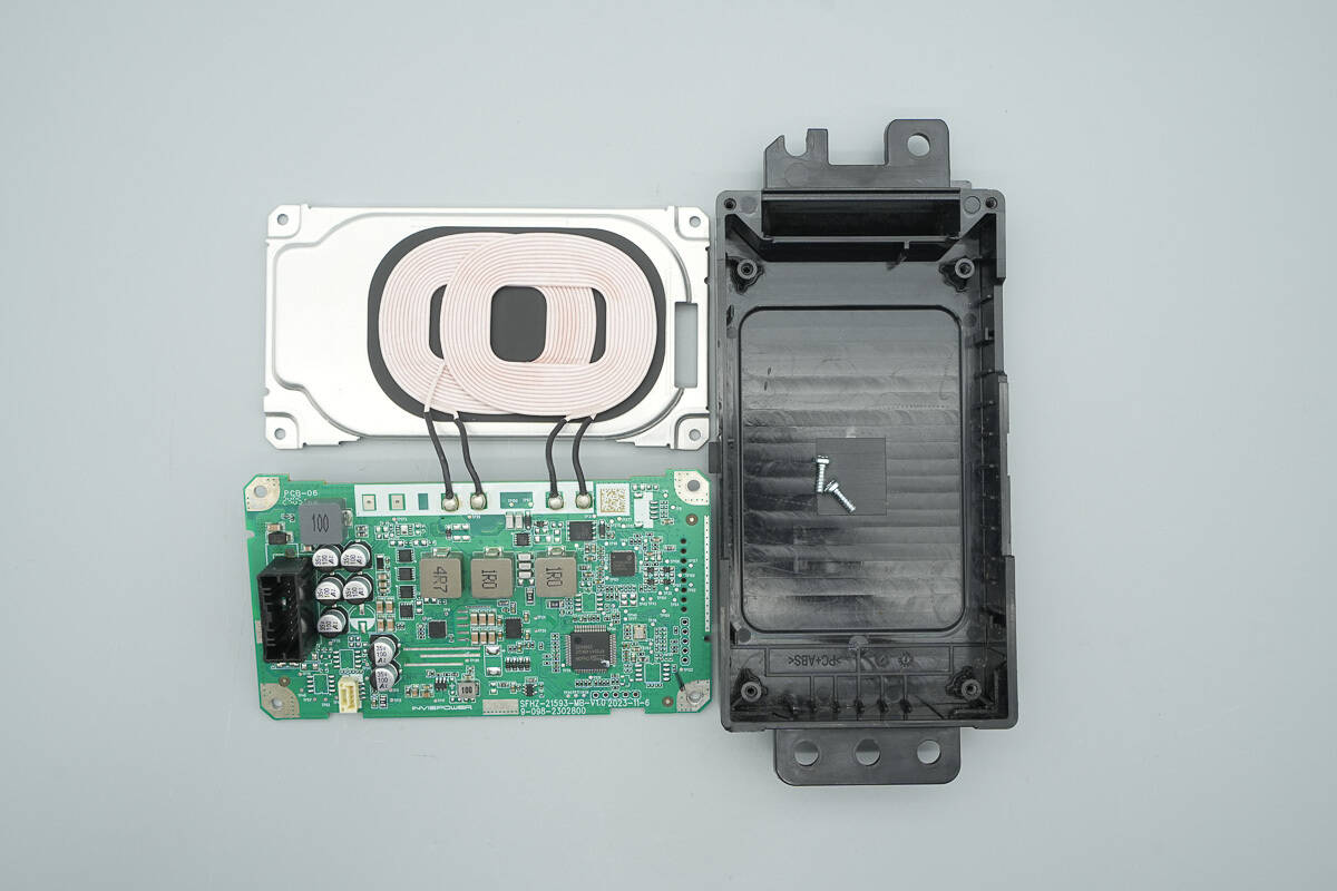
Remove the PCBA module and the wireless charging coil.
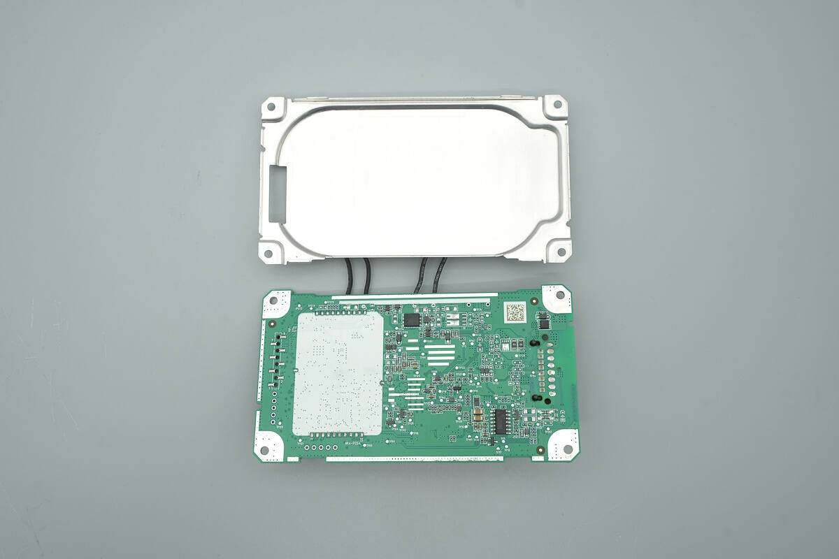
The charging coil is fixed on the metal shielding.
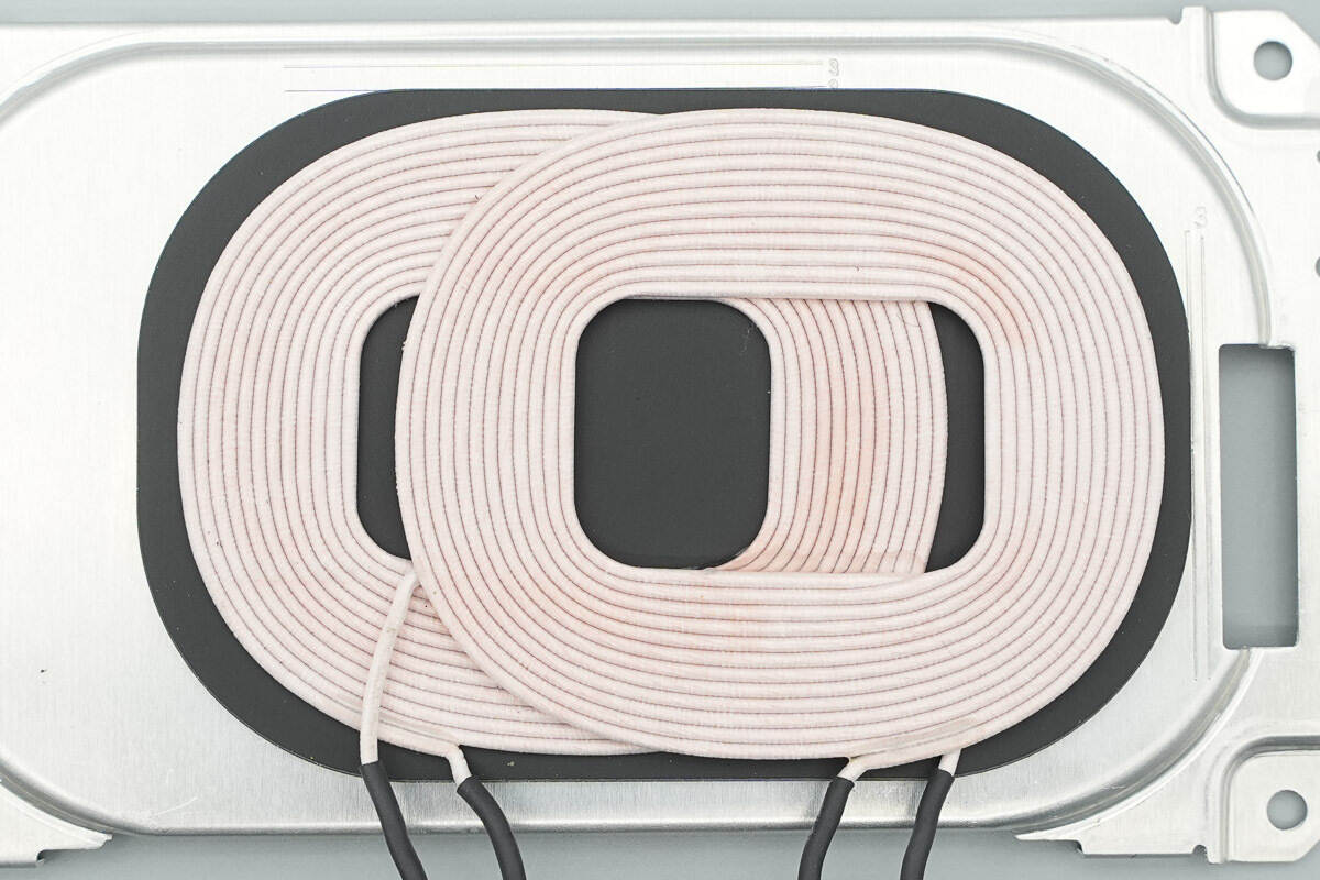
The coil is wound with enamel-coated wire, and the bottom is equipped with a magnetic insulation sheet. The leads are insulated with heat-shrink tubing.

The front of the PCBA module features a power input socket, filter inductors, filter capacitors, a synchronous buck-boost controller, synchronous buck-boost MOSFETs, alloy inductors, a wireless charging master control chip, a wireless charging power stage chip, and the main control MCU.

The back side of the PCBA is soldered with the coil switching MOSFETs and the CAN transceiver.
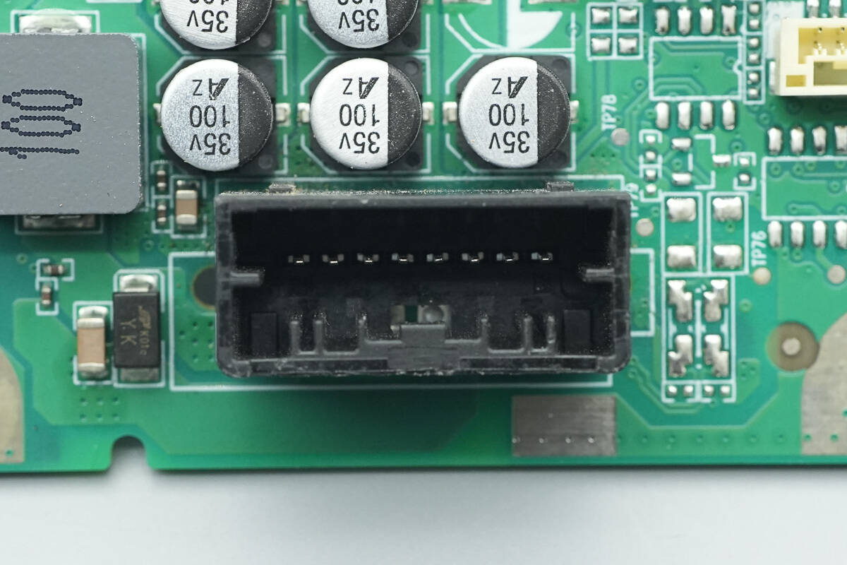
Close-up of the power input socket.

The input TVS diode is from SPSEMI, marked with YK, model SMAJ30CA, with a clamping voltage of 30V. It is used for input overvoltage protection and comes in a DO-214AC package.
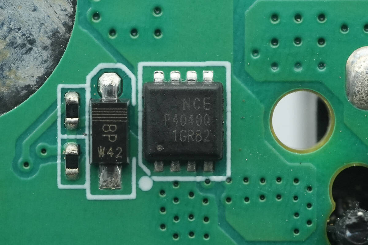
The MOSFET used for power control is from NCE, model NCEAP4040Q. It is AEC-Q101 certified, an NMOS with a voltage rating of 40V, a Rds(on) of 7.7mΩ, and comes in a PDFN 3.3×3.3-8L package.

The 10μH alloy inductor is used for input filtering.

There are a total of 7 filter capacitors, each with a specification of 35V 100μF.
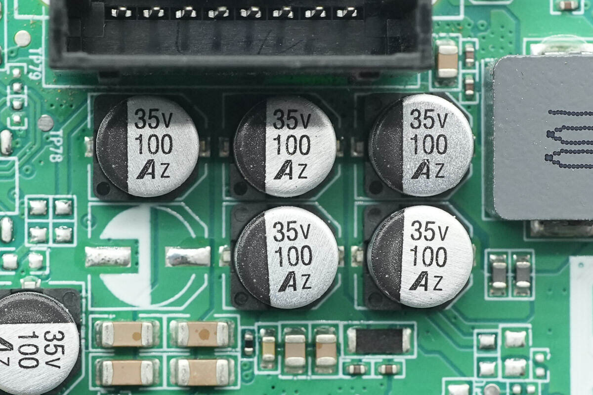
These five capacitors are used for input filtering, while the two capacitors on the left are used for output filtering.

The synchronous buck-boost controller is from SouthChip, model SC8701Q, which is an automotive-grade AEC-Q100 Level 1 version, supporting an operating temperature range of -40 to 125°C. The SC8701Q is a synchronous 4-switch buck-boost controller that effectively regulates the output voltage, whether the input voltage is higher, lower, or equal to the output voltage. It supports a wide input and output voltage range, from 2.7V to 36V for input and 2V to 36V for output.
The driver voltage is set to 10V to fully leverage the external MOSFETs for maximum efficiency. The switching frequency can be set between 200kHz and 600kHz and supports dynamic adjustment of output voltage and current limit. It also includes input and output overcurrent protection and over-temperature protection to ensure system safety. The chip operates within a temperature range of -40 to 125°C and comes in a QFN-32 package.
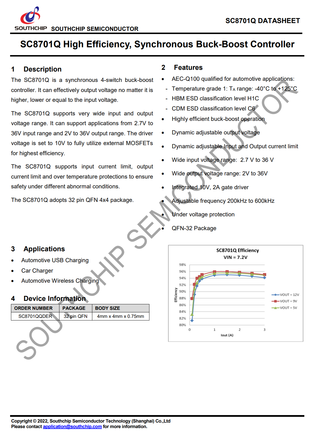
Here is the information about SouthChip SC8701Q.
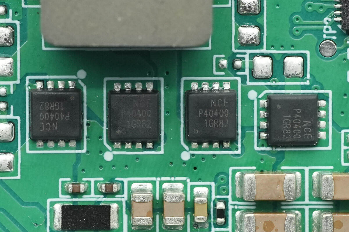
The synchronous buck-boost MOSFETs are from NCE, model NCEAP4040Q.

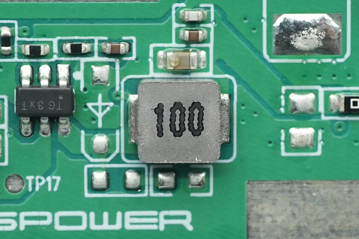
The 4.7μH alloy inductor is used for buck-boost conversion.
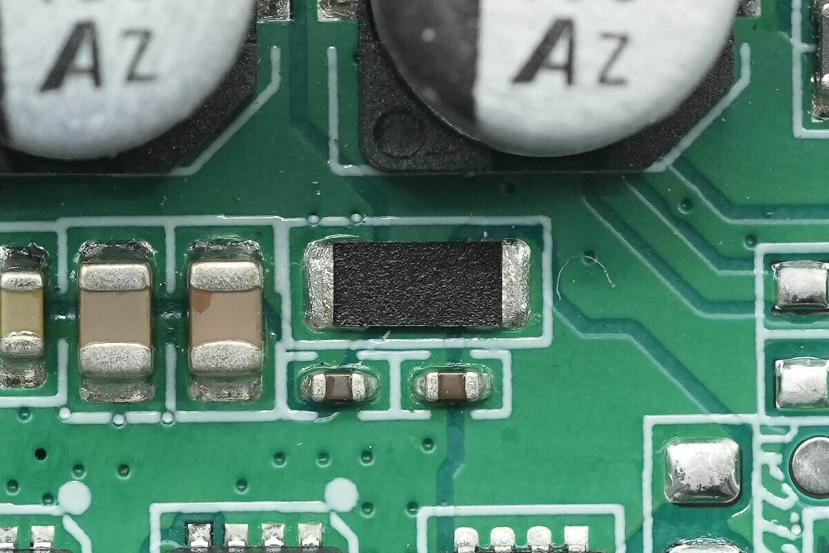
The current sensing resistor is used for input current detection.

The other current sensing resistor is used for output current detection.

The output filter capacitors have a specification of 35V 100μF.
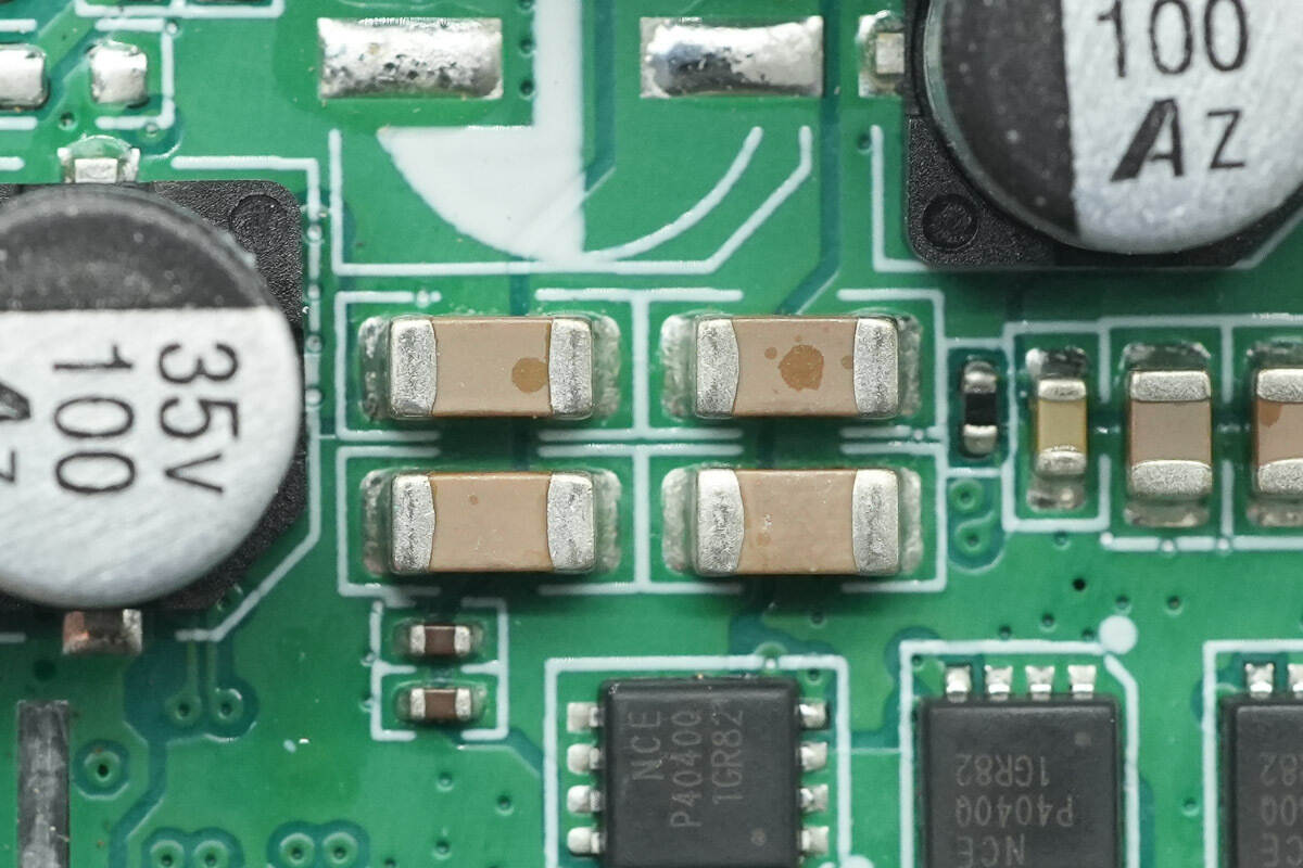
The four MLCC filter capacitors are connected in parallel.
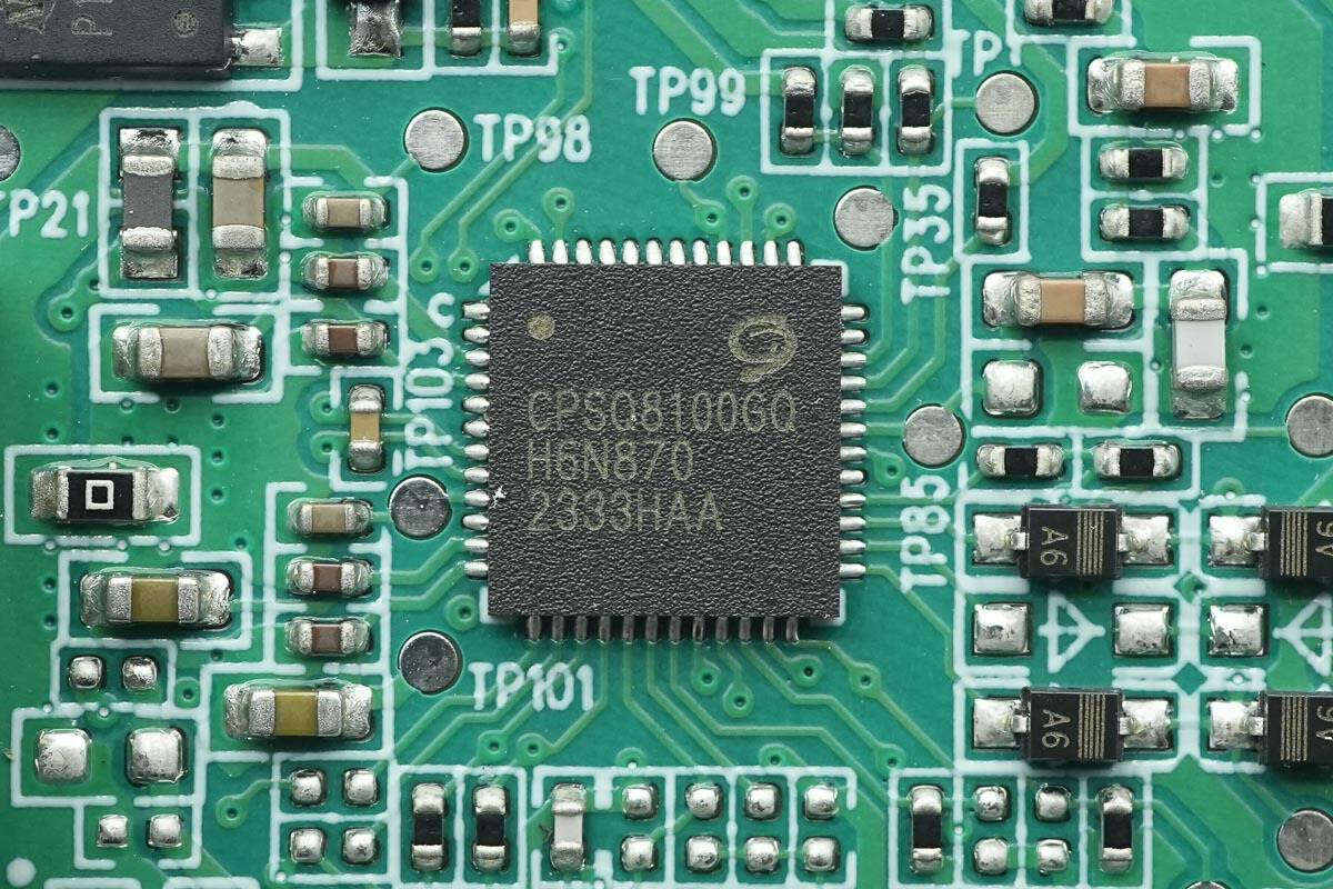
The wireless charging master control chip is from CPS, model CPSQ8100. It is a highly efficient and highly integrated wireless charging transmitter chip that supports 50W proprietary protocol wireless charging. The chip integrates a 32-bit MCU core, full-bridge driver circuits, Q-factor detection circuitry, and modulation-demodulation circuitry, minimizing the need for external components.
The internal memory supports read/write protection and features I2C and UART communication interfaces. It includes three half-bridge drivers, which can be configured for synchronous buck or synchronous boost operation. Additionally, the chip provides hardware overvoltage/undervoltage protection, overcurrent protection, and overtemperature protection. It meets AEC-Q100 Grade 2 certification and comes in a QFN48 package.
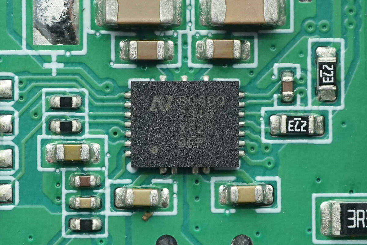
The wireless charging power stage chip is from NuVolta, model NU8060QH. It is a highly integrated, high-efficiency, and high-precision wireless charging transmitter chip that meets AEC-Q100 Grade 1 standards. The chip supports a wide input voltage range, with a recommended maximum operating voltage of 27V and a transient voltage tolerance of up to 36V. A single chip can support up to 80W wireless charging for the Rx load, enabling high-power wireless fast charging.
The NU8060QH integrates a 12mΩ low-resistance full-bridge and, compared to existing products on the market, offers exceptional thermal performance. It also integrates many essential features for wireless charging applications, such as full-bridge drive, 5V LDO, high-precision current sensing, Q-factor detection, and internal communication demodulation functions. The chip comes in a QFN21 package.
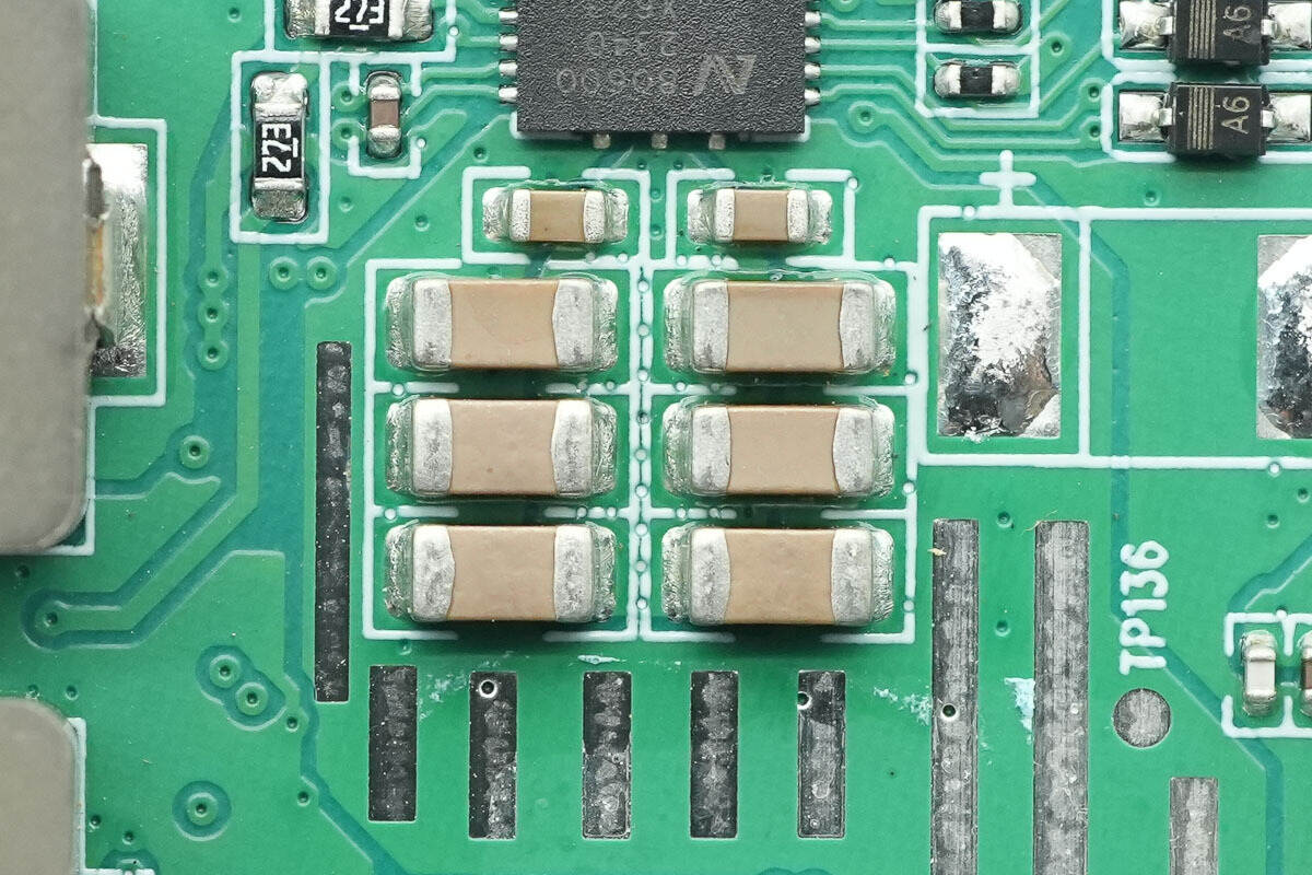
The chip's power supply input is filtered using MLCC capacitors.
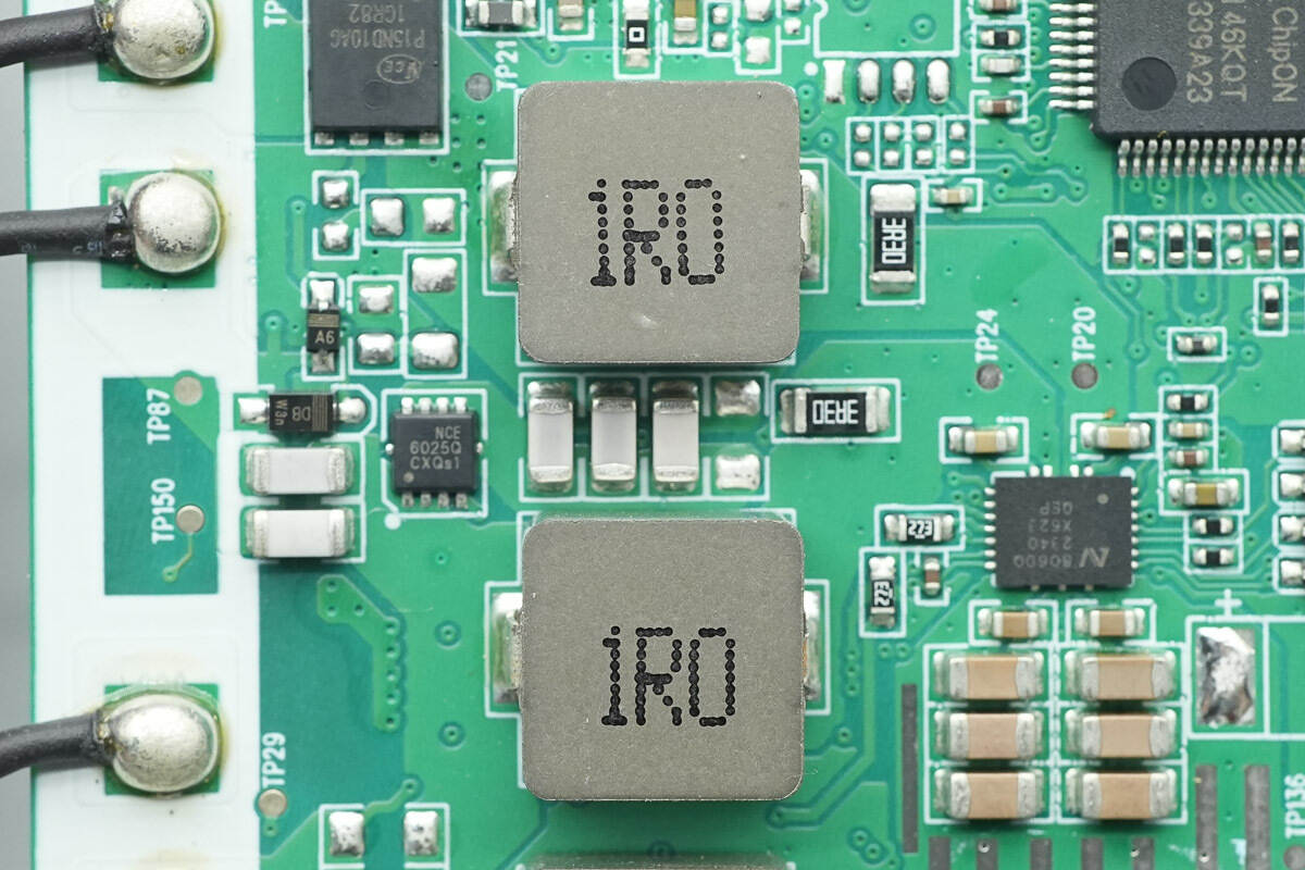
Two 1μH alloy inductors are used for output filtering.
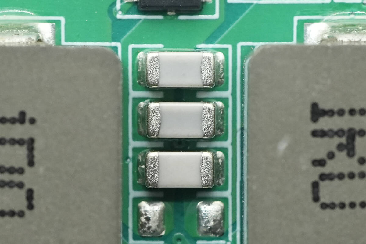
There are resonant capacitors placed between the inductors.
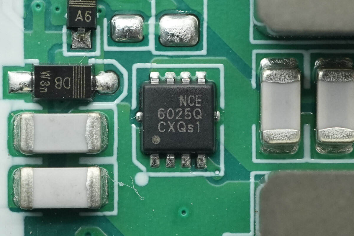
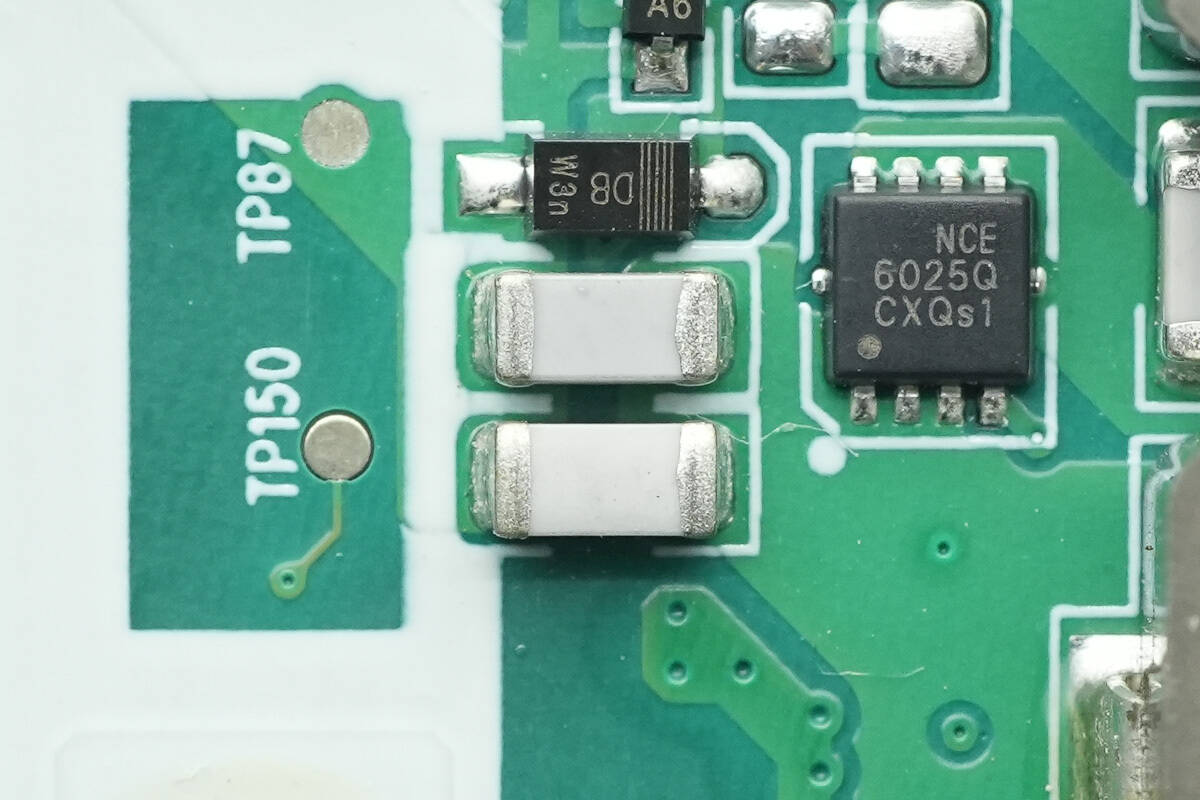
The MOSFET used for switching the resonant capacitor is from NCE, model NCEA6025Q. It is AEC-Q101 certified, an NMOS with a voltage rating of 60V, a Rds(on) of 12mΩ, and comes in a PDFN 3.3×3.3-8L package.
Close-up of the two NPO resonant capacitors.
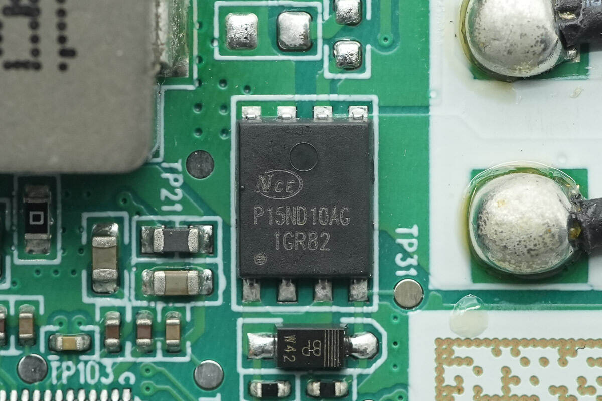
The MOSFET used for wireless charging coil switching is from NCE, model NCEAP15ND10AG. It is AEC-Q101 certified, a dual NMOS with a voltage rating of 100V, a Rds(on) of 12.5mΩ, and comes in a PDFN 5×6-8L package.
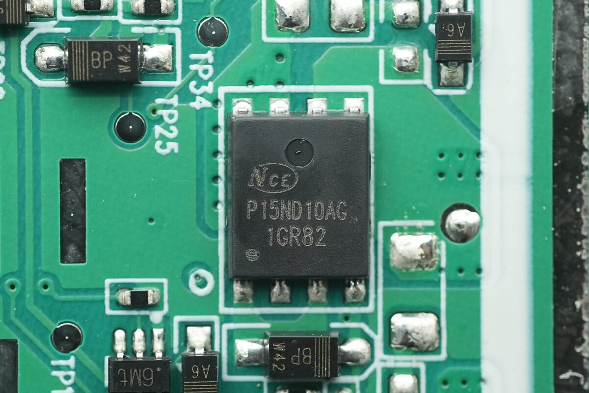
The other MOSFET for coil switching has the same model.

The synchronous buck chip is from DIODES, marked with TG, model AP64060. It is a synchronous buck converter with an input voltage range of 4.5V to 40V. The chip integrates the MOSFETs and supports an output current of up to 600mA, with a switching frequency of 2MHz. It comes in a TSOT26 package.
The 10μH inductor is used in conjunction with the buck converter.
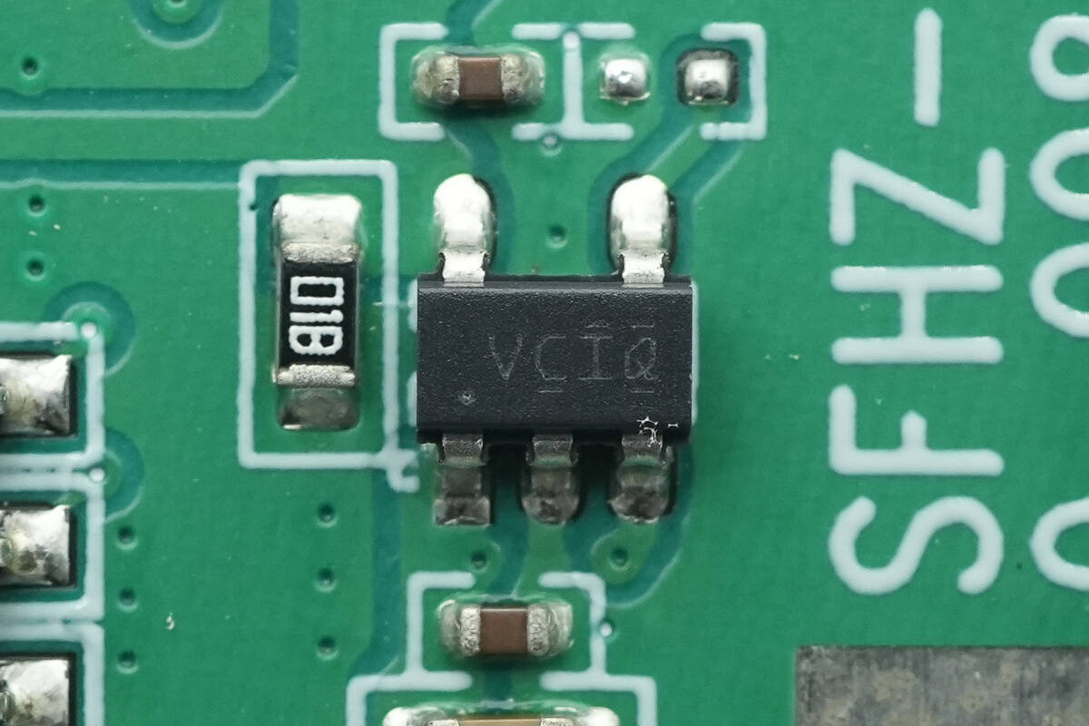
The regulator chip is from TI, marked with VCIQ, model TLV73333P. It supports an input voltage range of 1.4V to 5.5V, with an output current of 300mA and an output voltage of 3.3V. The chip features power supply rejection (PSRR) and comes in an SOT-23 package.
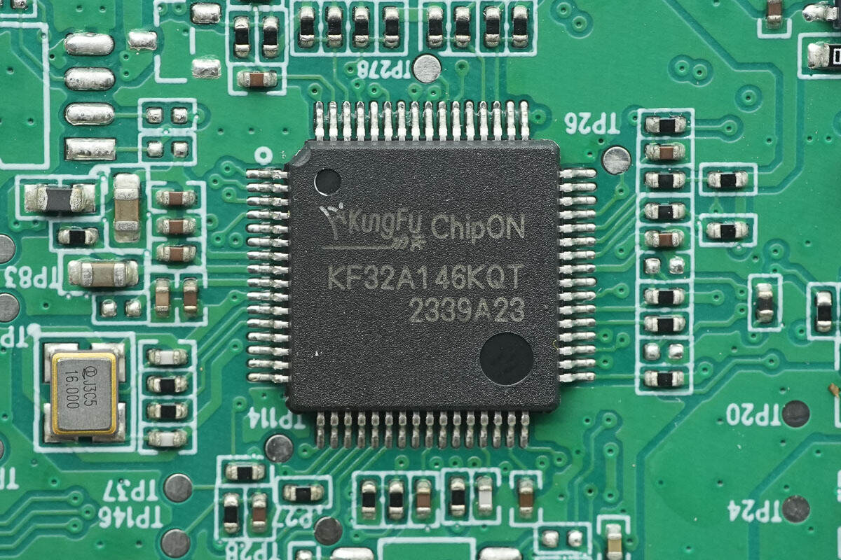
The MCU is from ChipON, model KF32A146KQT. It is an automotive-grade 32-bit MCU, featuring a high-performance KungFu32 core with a clock speed of up to 72MHz. The MCU is equipped with 256KB of FLASH memory, 48KB of RAM with ECC (Error Correction Code) protection, and 16KB of ROM. It supports various interfaces such as SPI, I2C, USART, and CAN, and operates within a voltage range of 2.7V to 5.5V. The chip comes in an LQFP64 package.
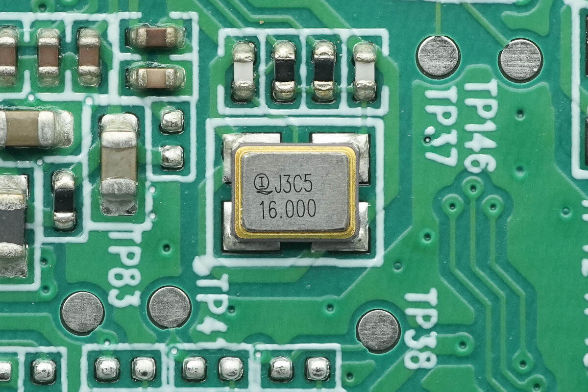
Close-up of the 16.000 MHz clock crystal oscillator.
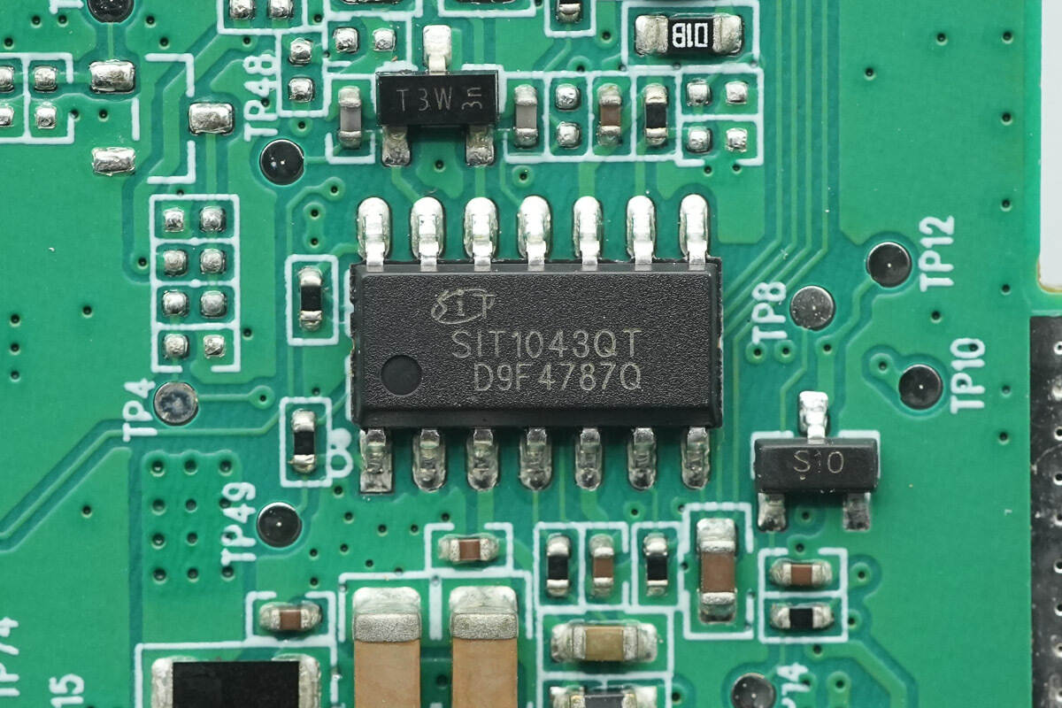
The CAN transceiver is from SiT, model SIT1043Q. It is AEC-Q100 certified and compatible with ISO 11989-2:2016 and SAE J2284-1 to SAE J2284-5 standards. The transceiver features low standby power consumption and a standby mode, with support for both remote and local wake-up functions. It supports a voltage tolerance of ±58V and is suitable for MCU applications with a 3.3V or 5V power supply. The chip comes in an SOP14 package.
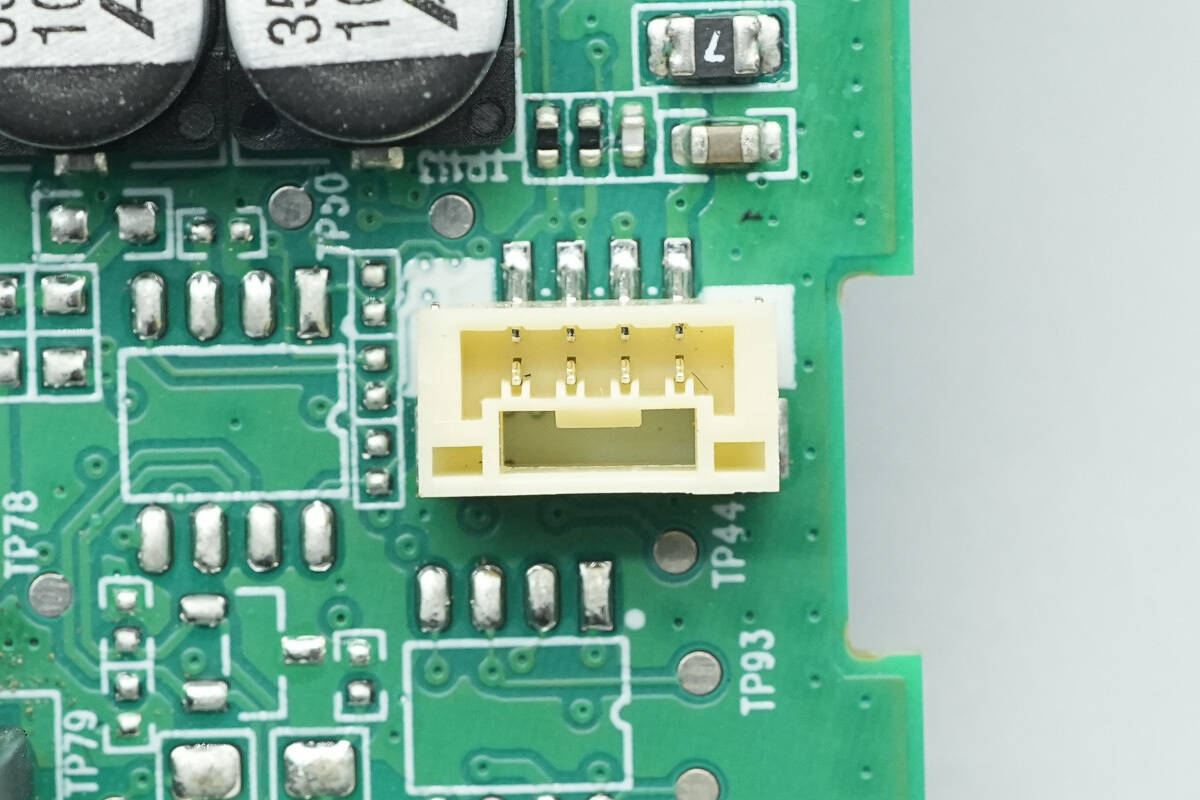
Close-up of the cooling fan connector.
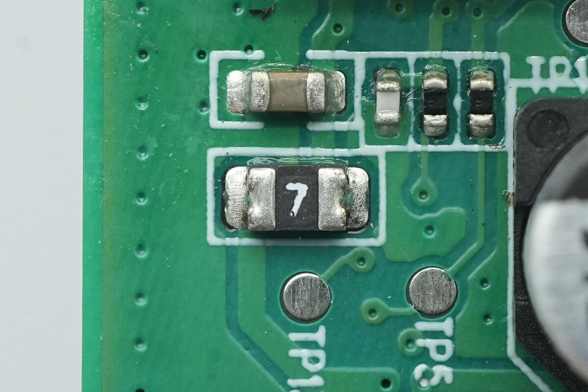
The fan power supply is equipped with a resettable fuse.

Well, those are all components of the BYD 50W In-Car Pre-installed Wireless Charging Module.
Summary of ChargerLAB
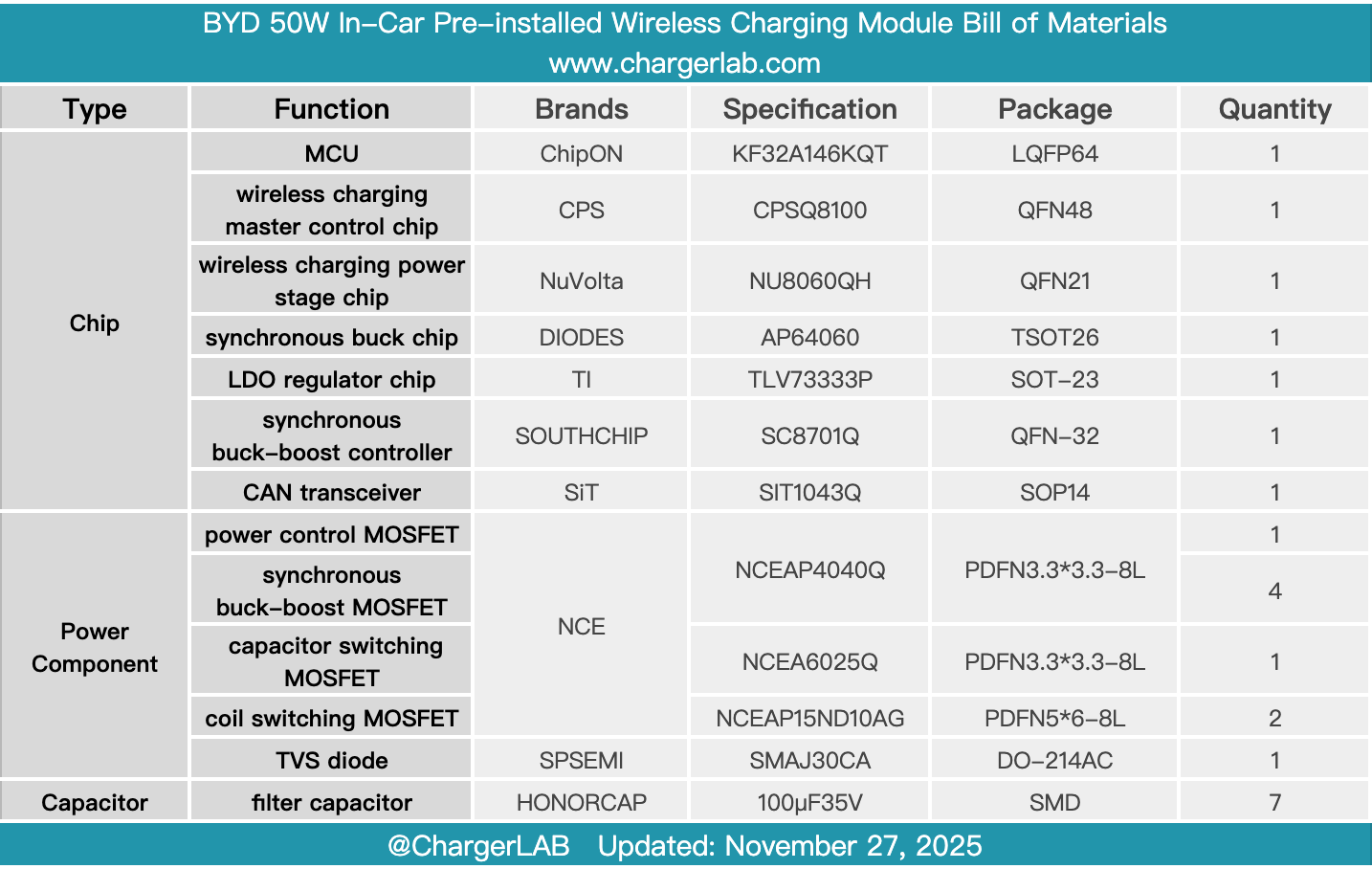
Here is the component list of the BYD 50W In-Car Pre-installed Wireless Charging Module for your convenience.
It features a single charging pad and supports 50W wireless output. The housing is made of galvanized steel, and it is equipped with a cooling fan to enhance the performance of high-power wireless charging.
After taking it apart, we found that it uses the CPS CPSQ8100 wireless charging master control chip paired with the NuVolta NU8060QH for wireless charging. The SouthChip SC8701Q synchronous buck-boost controller is used for voltage conversion, powering the wireless charging power stage chip. Automotive-grade MOSFETs from NCE are used for power control, synchronous buck-boost conversion, and coil switching, all of which are AEC-Q101 certified.
The MCU used is the ChipON KF32A146KQT, and the SiT SIT1043Q is employed for CAN communication. The DIODES AP64060 synchronous buck chip is used for power step-down conversion, while the TI TLV73333 pre-regulator chip provides power to the master control chip. Thermal pads are applied inside the housing to dissipate heat from the heat-generating components. The device utilizes automotive-grade components with solid craftsmanship and materials.
Related Articles:
1. Teardown of CUKTECH 10 100W Car Charger with Retractable Cable (CC903P)
2. Teardown of Belkin BoostCharge Pro 100W 3-Port GaN Wall Charger (WCH016yz)
3. Teardown of HONOR CHOICE 100W 20000mAh Power Bank (QHL-PB06)