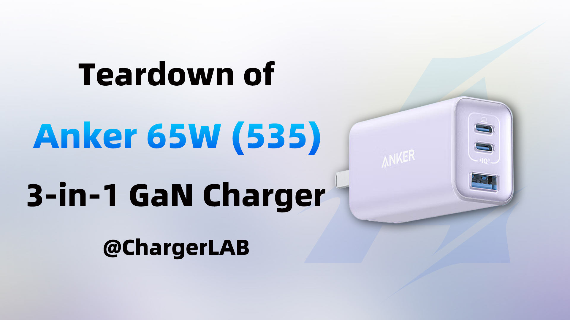
Introduction
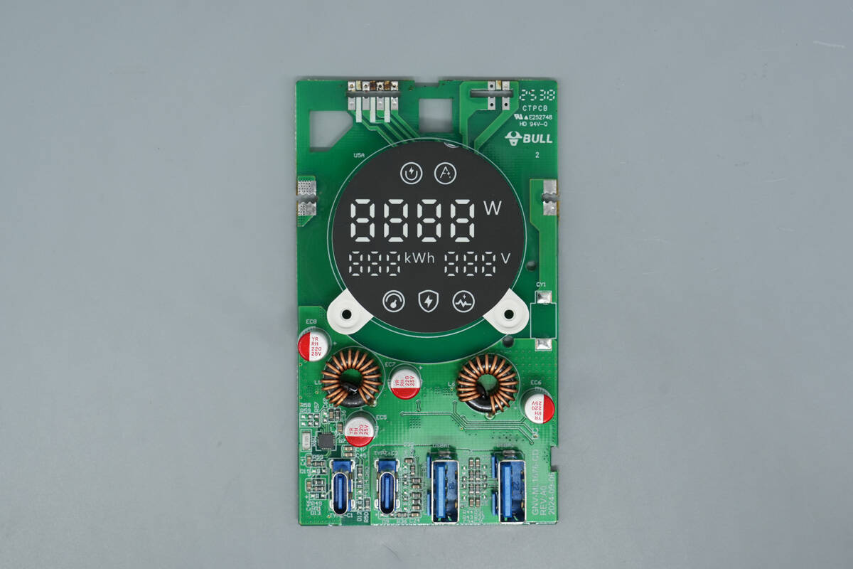
BULL has launched a 67W GaN digital-display fast-charging power strip that continues the brand’s tradition of high quality and safety in outlets, while innovatively adding a smart digital display. The product is cube-shaped and equipped with two USB-C ports and two USB-A ports, supporting a maximum output of 67W.
The smart digital display provides real-time readings of power draw, energy consumption, and input voltage. The top surface features a one-key master micro-switch for convenient operation and protection against accidental activation. Next, we examine the product’s internal structure and material quality.
Product Appearance
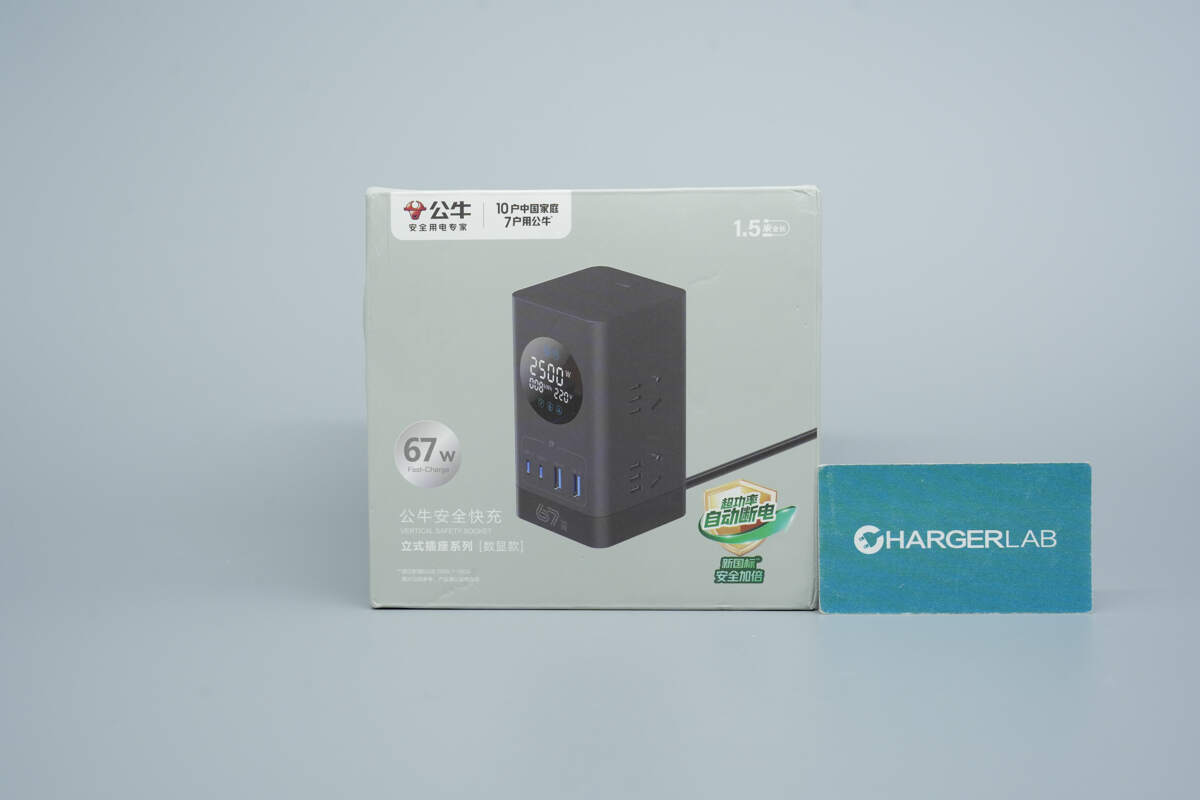
The front of the packaging box features the BULL brand, the product name, the appearance/design, and other details.
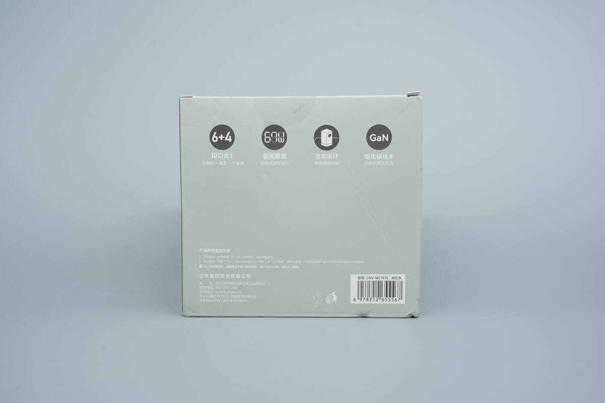
The back displays the product’s selling points and the merchant’s information.
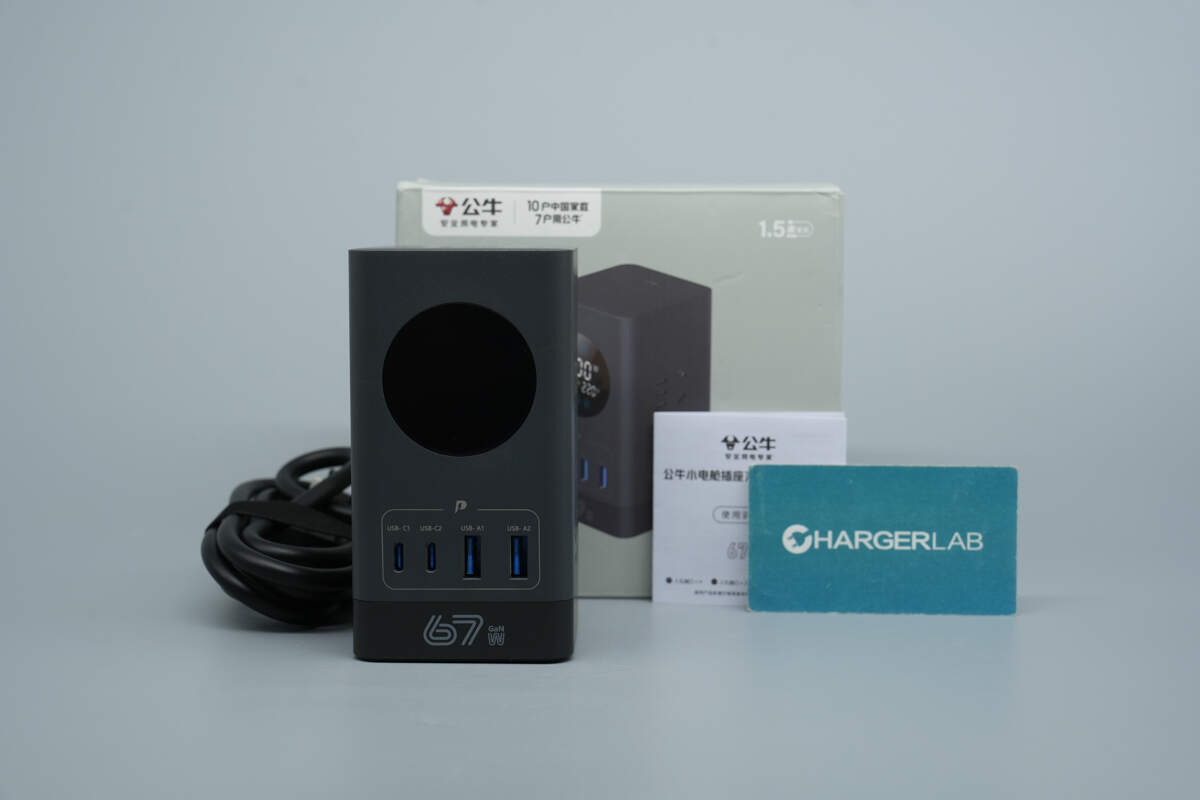
The package includes the power strip and the user manual.
The outer shell is made of highly flame-retardant material and can pass the 750°C glow wire test. The surface is frosted, and the style is simple.
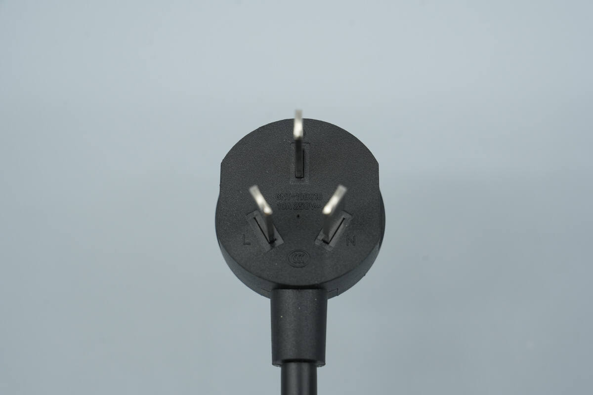
The power cord uses a three-pin plug and is grounded.
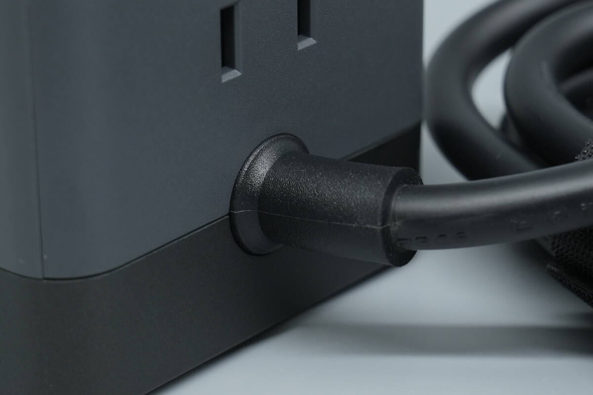
The cable-to-body connection is designed to resist bending.
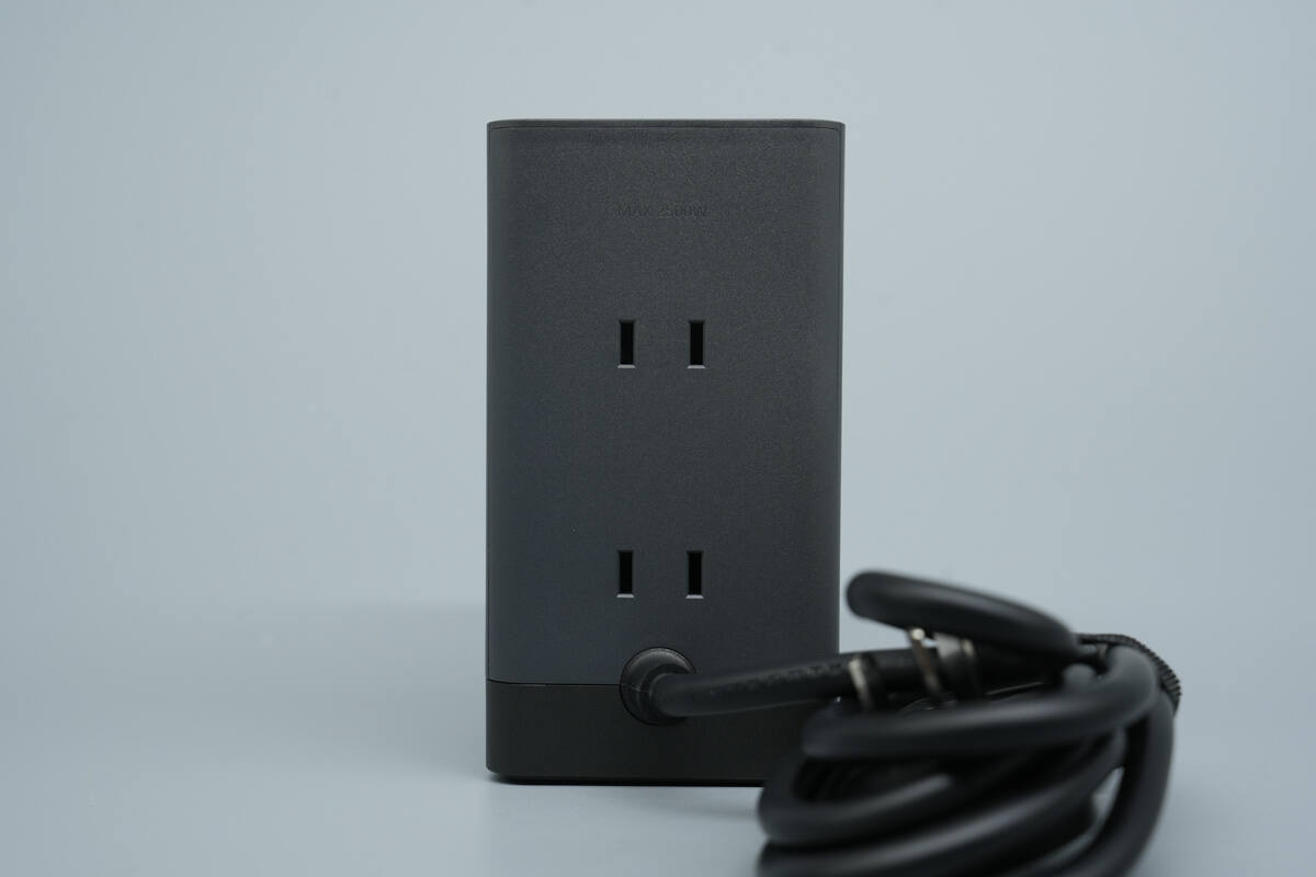
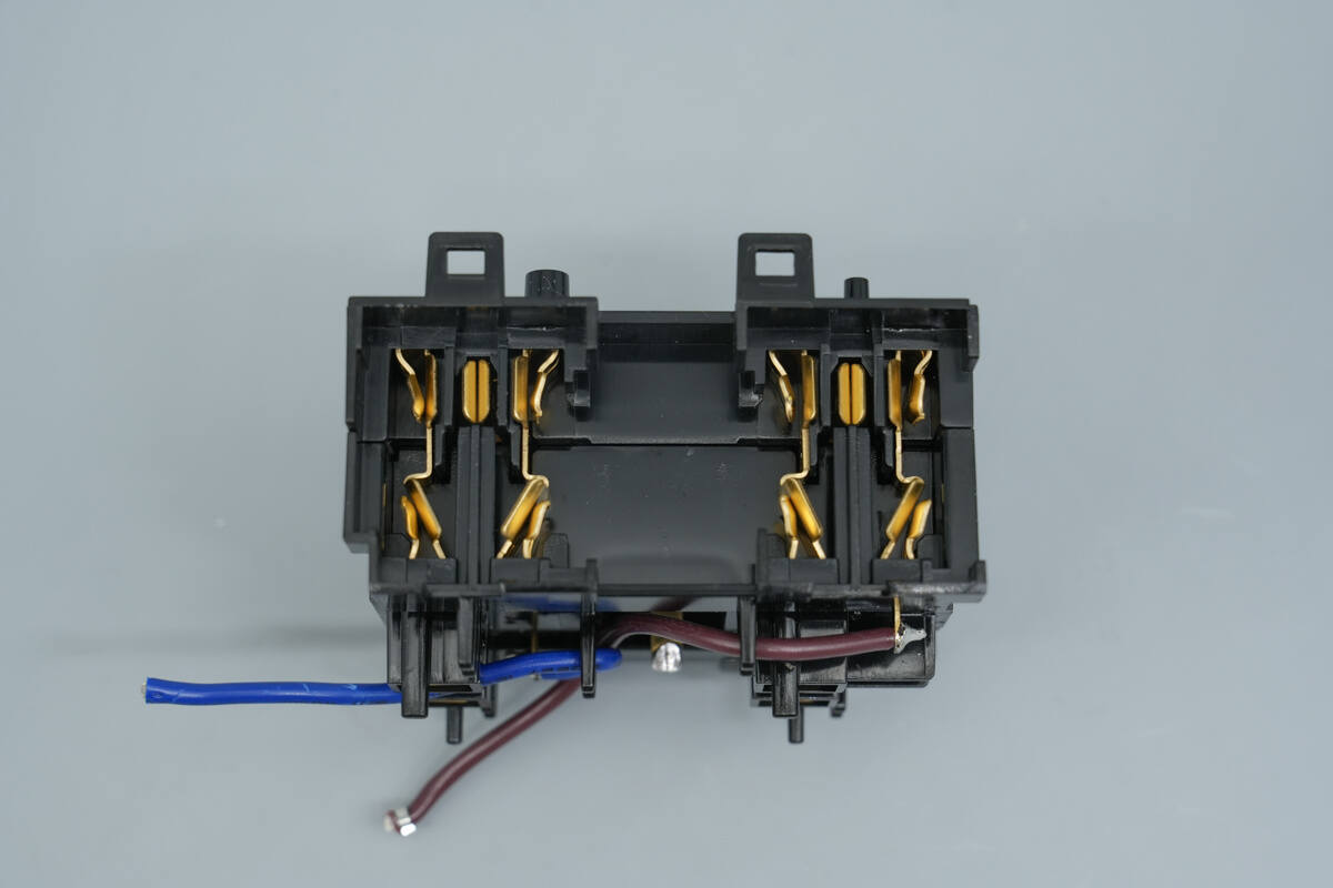
The rear of the device features two sets of dual-prong AC outlets.
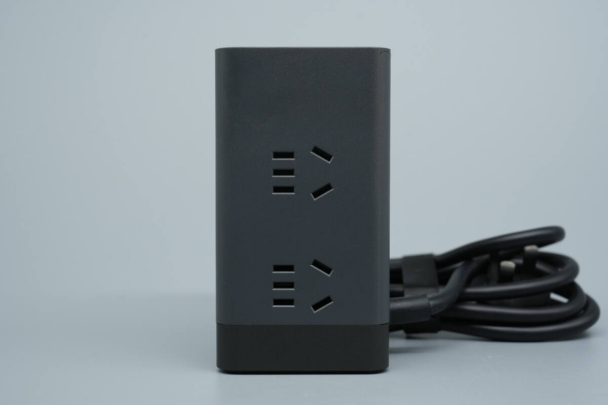
Two 3+2 combination outlets are provided on each side.
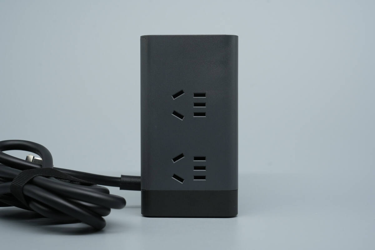
On the other side, at a glance. The AC outlets are equipped with safety shutters to effectively prevent foreign objects from being inserted into the individual outlets.
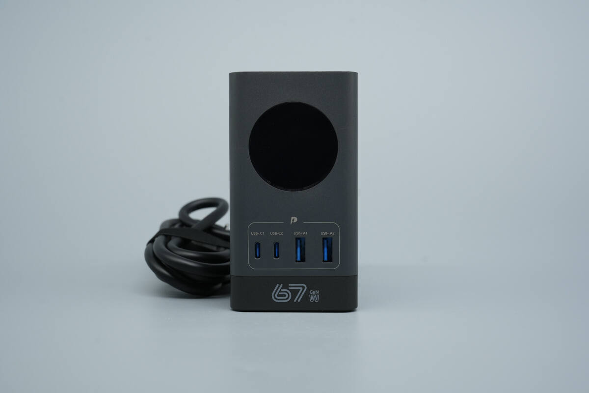
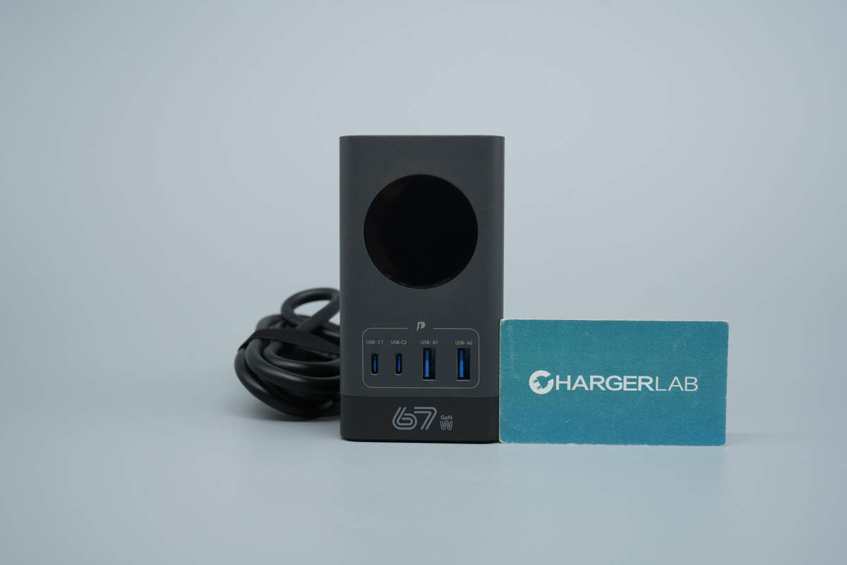
The front features a digital display and two USB-C ports as well as two USB-A ports.
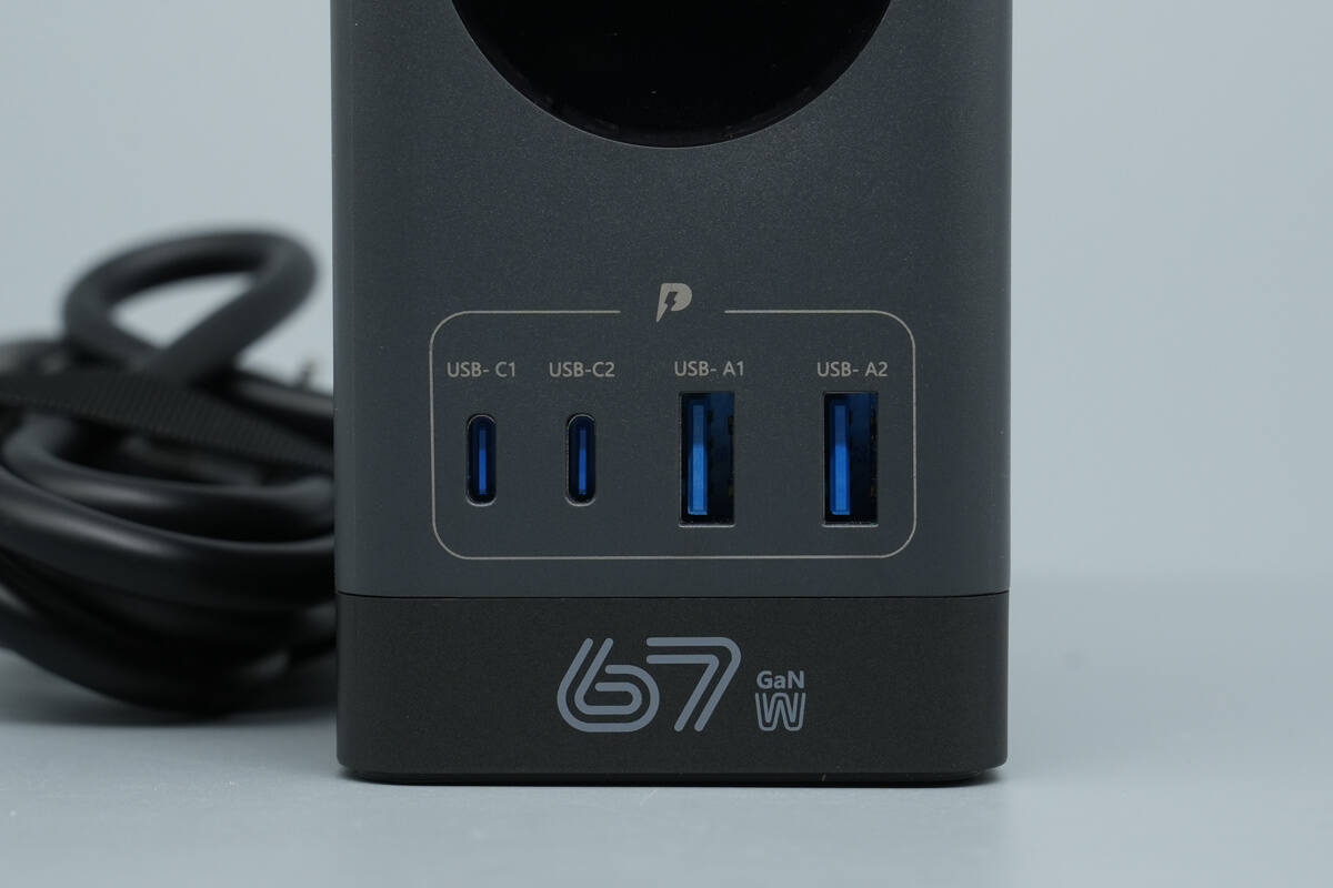
Each port is labeled with its corresponding number.
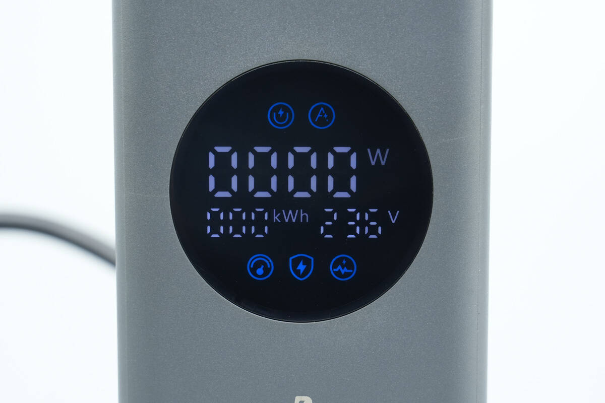
The smart digital display can show power consumption, energy usage, input voltage, and various protection alerts.
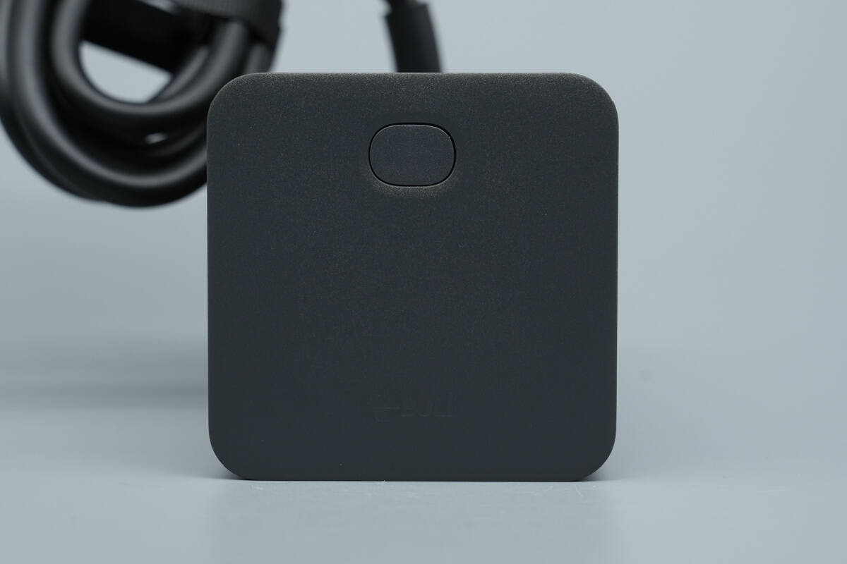
A micro switch is located at the top, enabling simple one‑button master control.
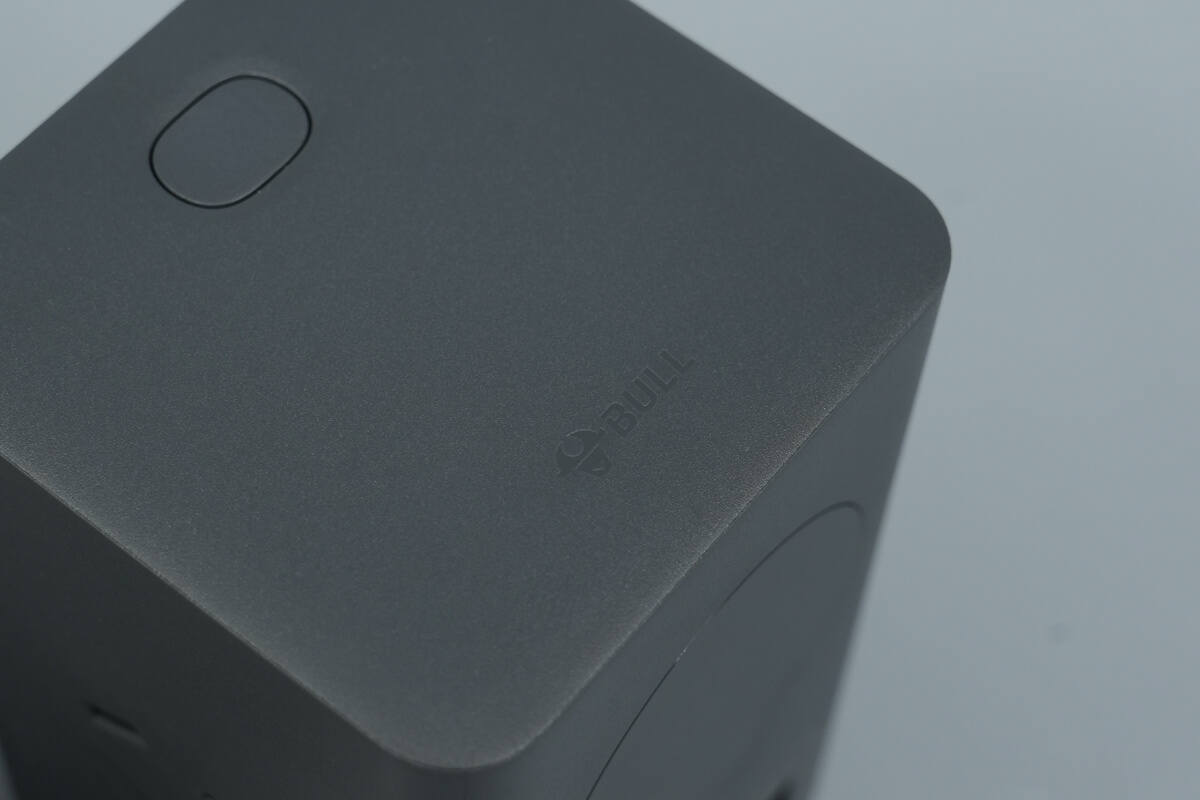
The Bull logo is also featured on the top edge.
The bottom features protective pads that securely grip the desk.
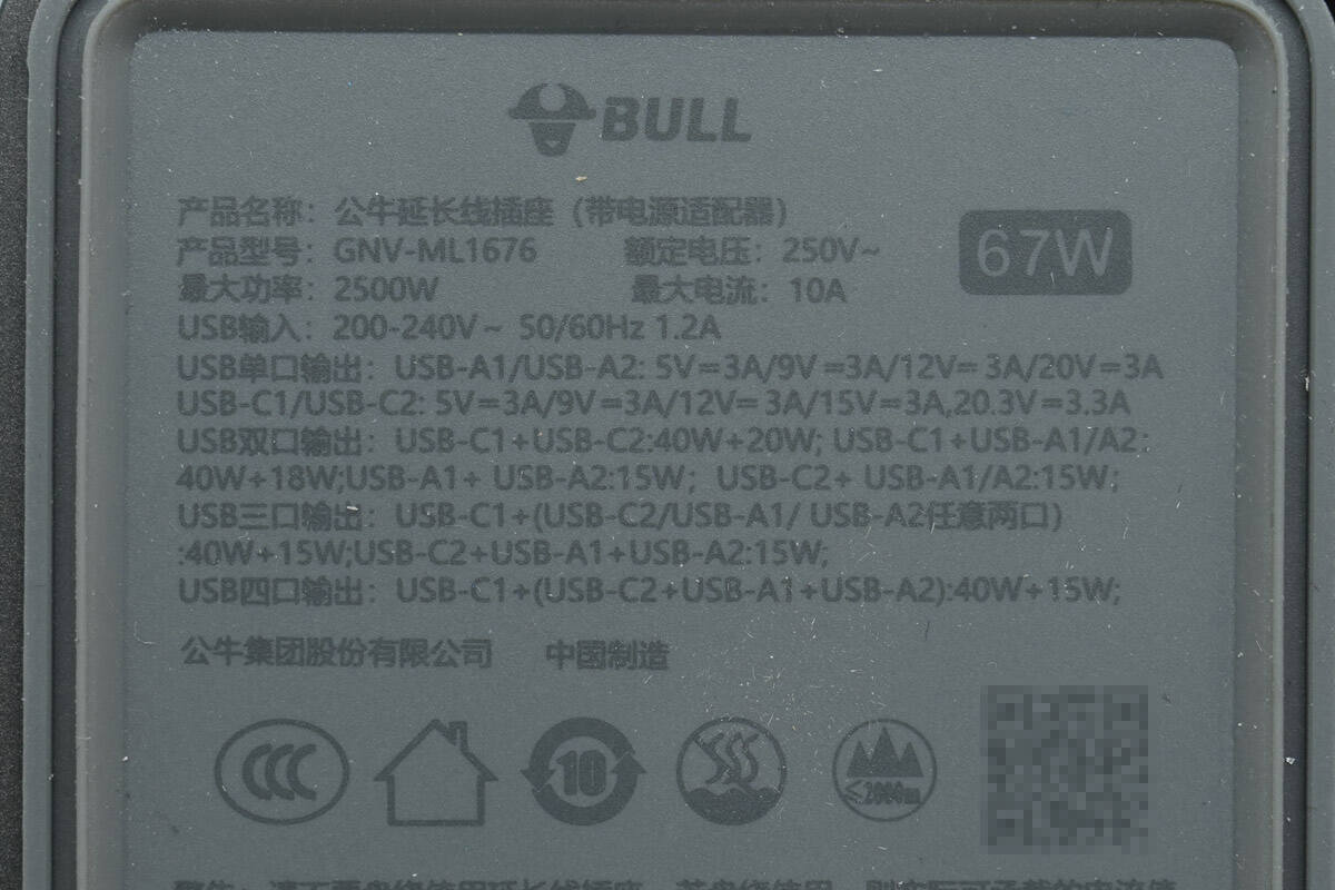
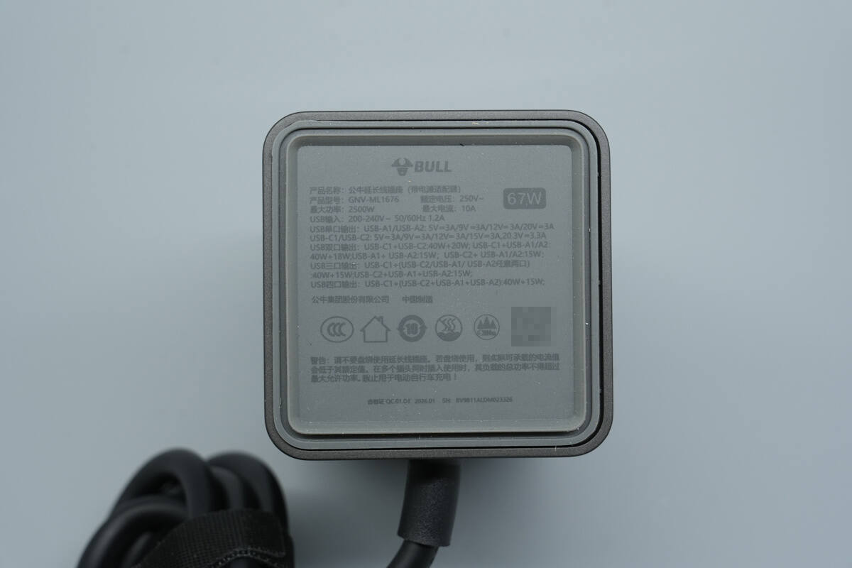
Model: GNV-ML1676
Rated voltage: 250V~
Maximum power: 2500W
Maximum current: 10A
USB input: 200-240V~ 50/60Hz 1.2A
USB single-port output:
USB-A1/A2: 5V 3A, 9V 3A, 12V 3A, 20V 3A
USB-C1/C2: 5V 3A, 9V 3A, 12V 3A, 15V 3A, 20.3V 3.3A
USB dual-port output:
USB-C1+USB-C2: 40W + 20W
USB-C1+USB-A1/A2: 40W + 18W
USB-C2+USB-A1/A2: 15W
USB-A1+USB-A2: 15W
USB triple-port output:
USB-C1+(USB-C2/USB-A1/USB-A2 ): 40W + 15W
USB-C2+USB-A1+USB-A2: 15W
USB quadruple-port output:
USB-C1+(USB-C2+USB-A1+USB-A2): 40W + 15W
CCC certified.
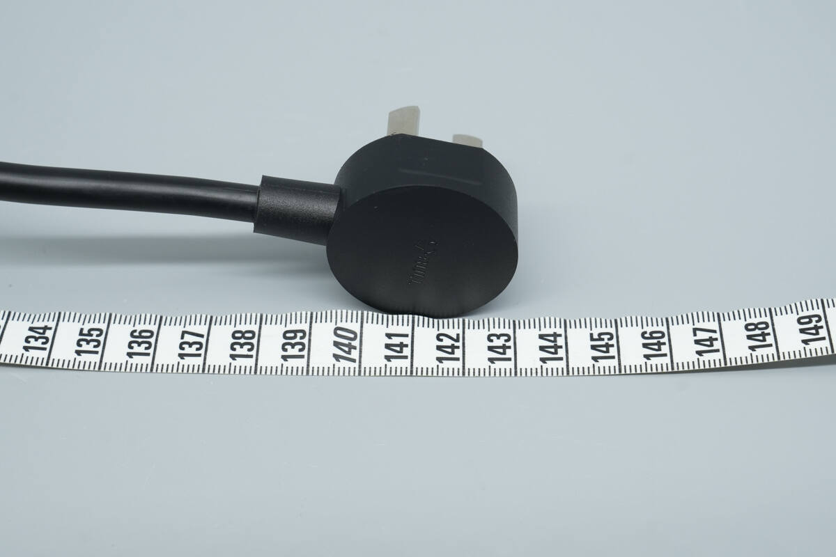
The length of the cable is about 143 cm (56.3 inches).
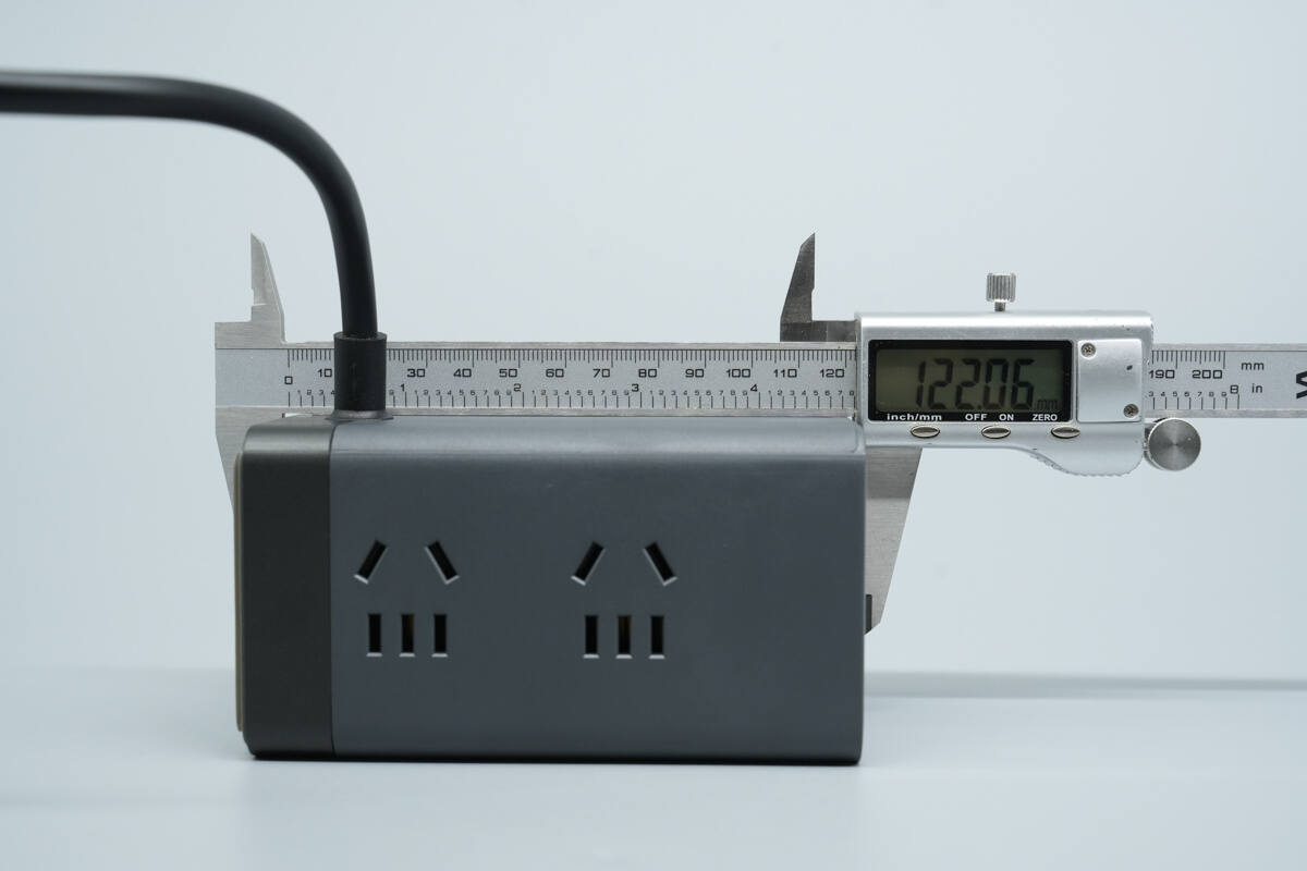
The height of the power strip is about 122.06 mm (4.81 inches).
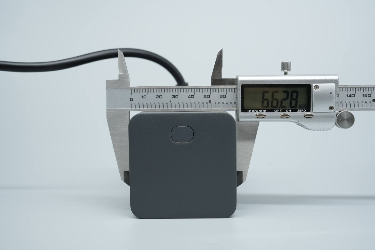
The width is about 66.28 mm (2.61 inches).
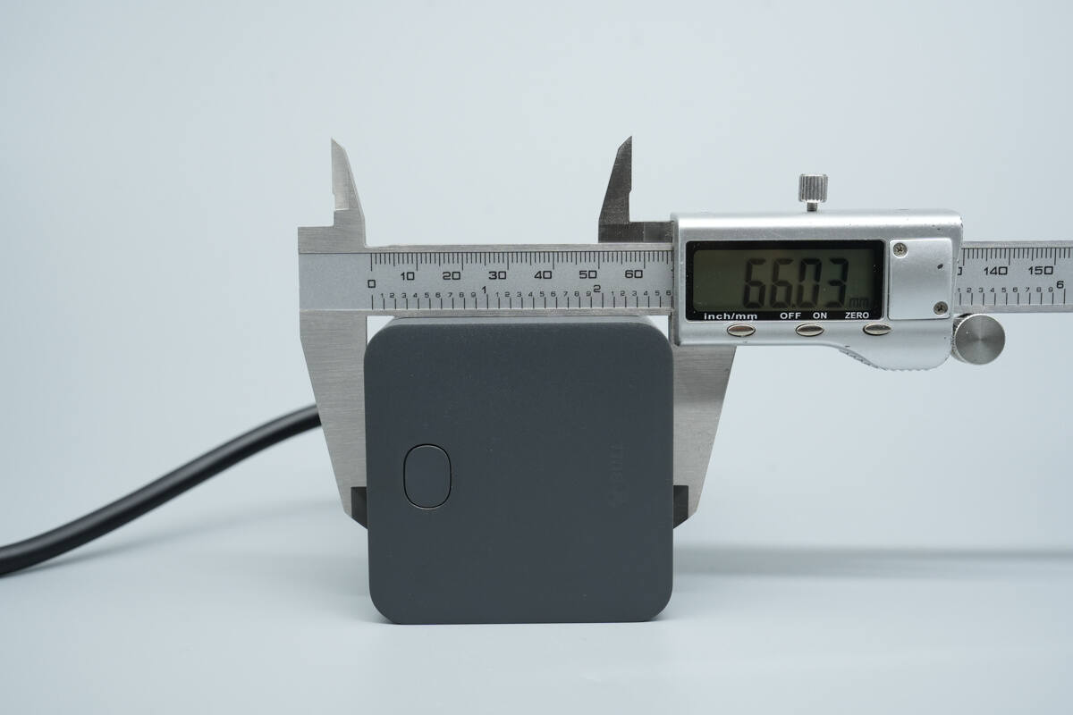
The thickness is about 66.03 mm (2.6 inches).
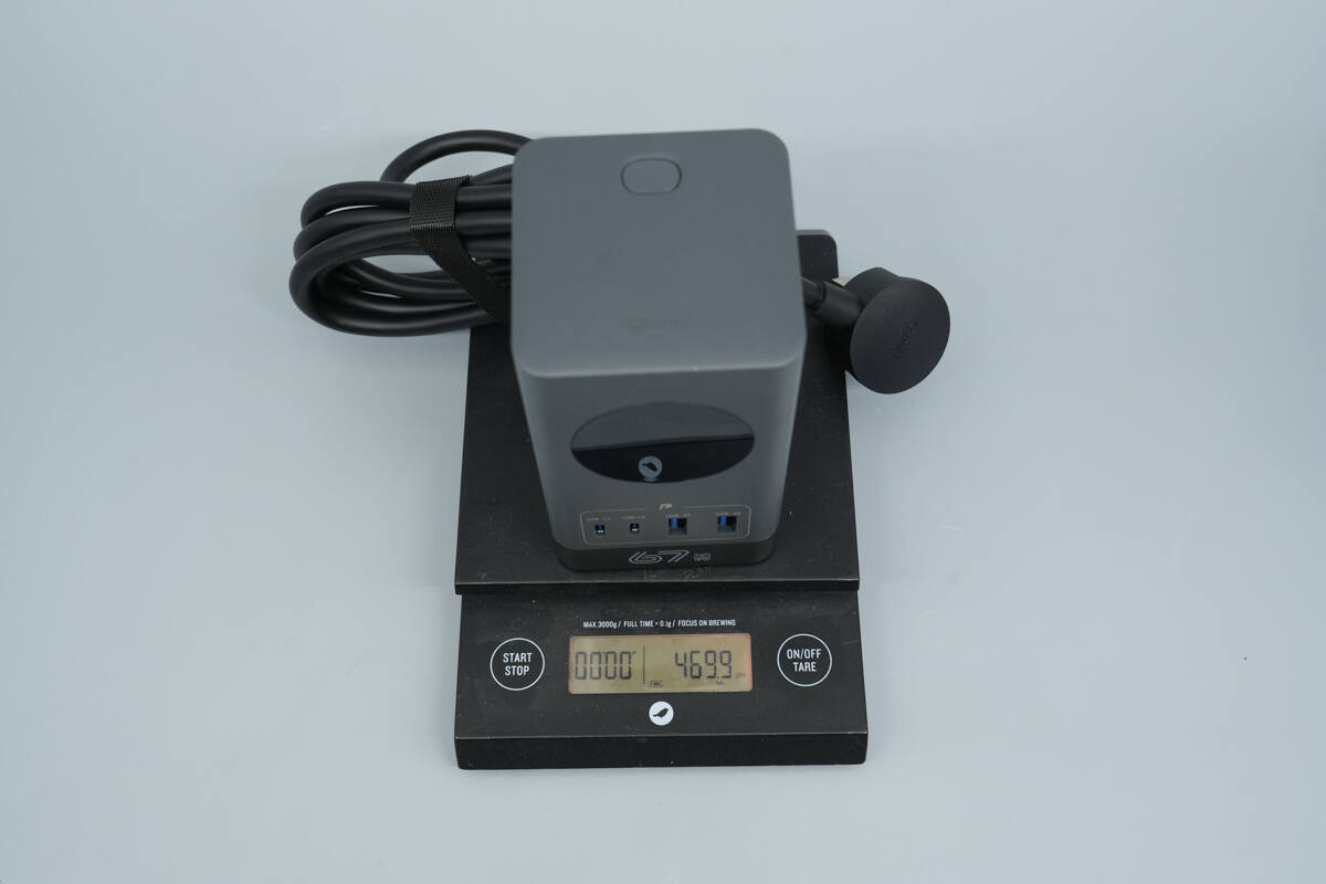
The weight is about 470 g (16.58 oz).
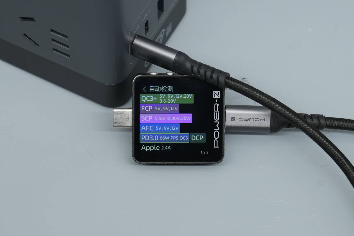
ChargerLAB POWER-Z KM003C shows that the USB-C1 port supports QC3+/5, FCP, SCP, AFC, PD3.0, PPS, DCP, and Apple 2.4A charging protocols.
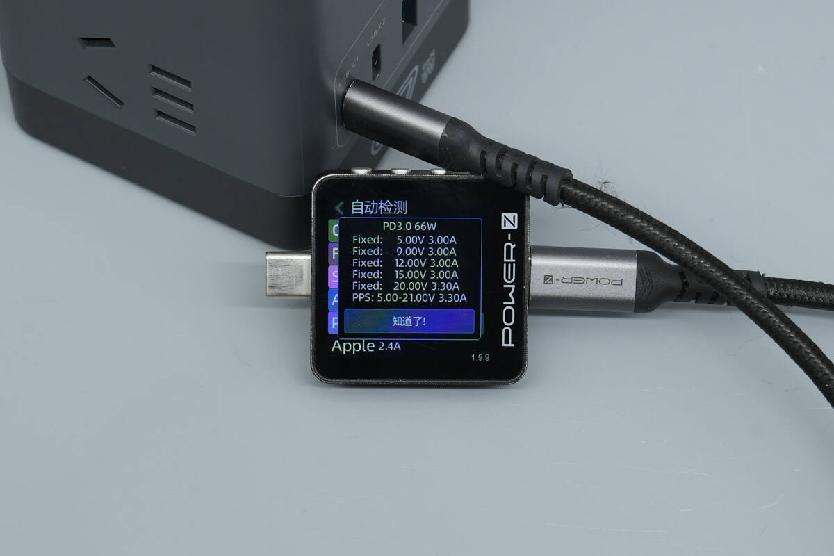
It features five fixed PDOs of 5V3A, 9V3A, 12V3A, 15V3A, 20V3.3A, along with a 5-21V3.3A PPS voltage range.
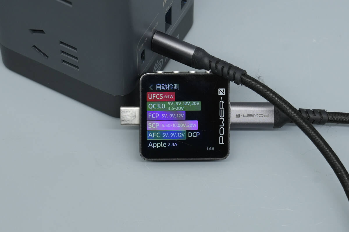
The USB-C2 port supports UFCS, QC3.0, FCP, SCP, AFC, DCP, and Apple 2.4A charging protocols.
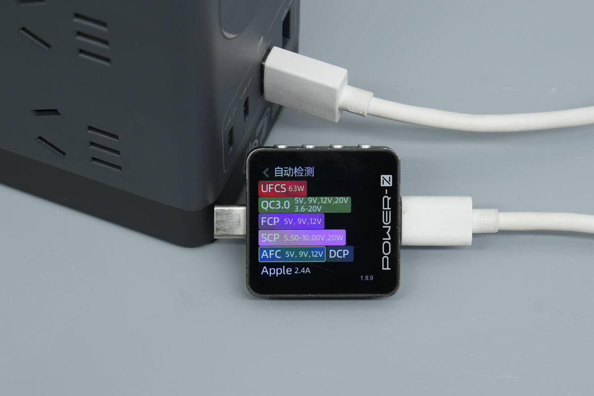
The USB-A1 port supports UFCS, QC3.0, FCP, SCP, AFC, DCP, and Apple 2.4A charging protocols.
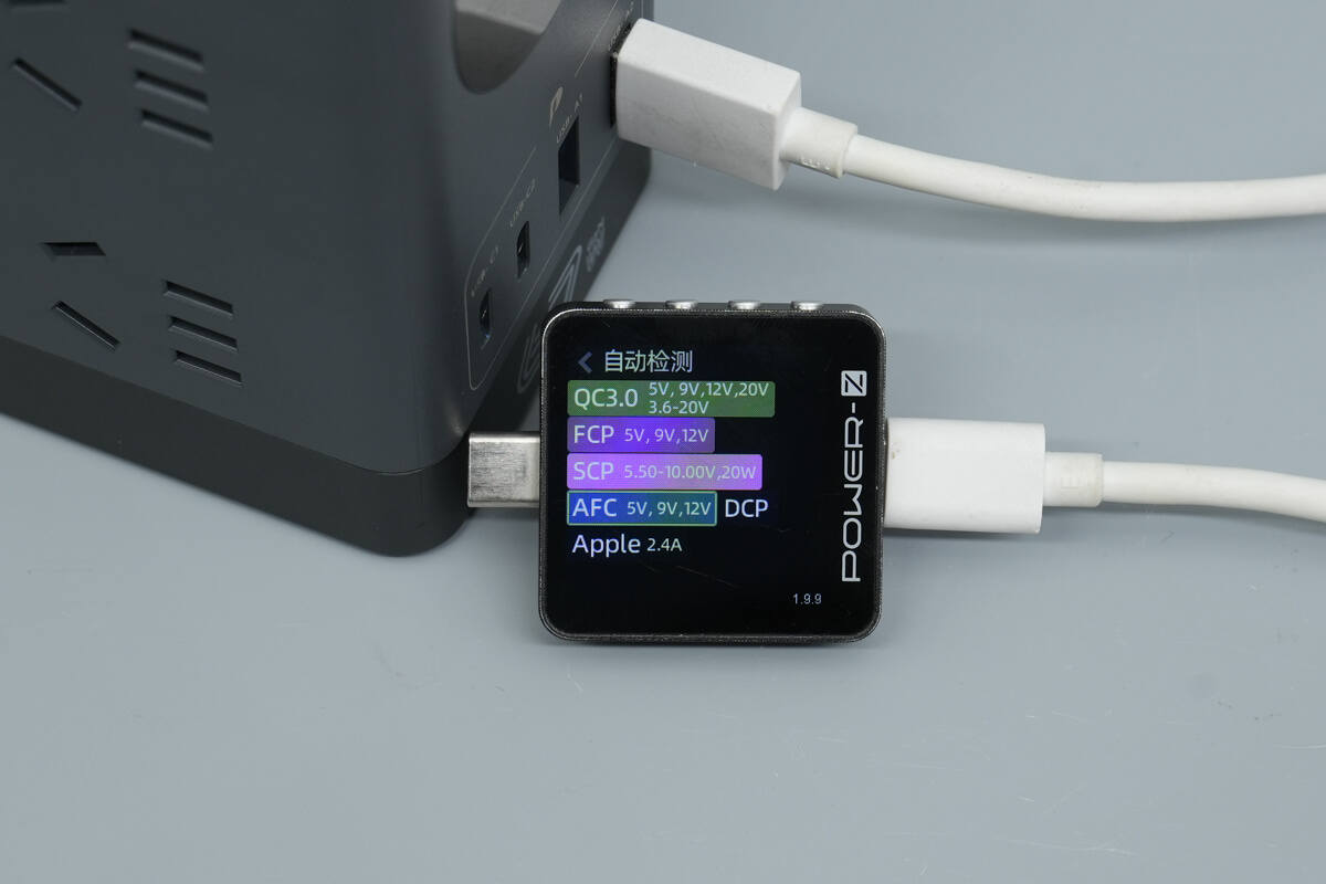
The USB-A2 port supports QC3.0, FCP, SCP, AFC, DCP, and Apple 2.4A charging protocols.
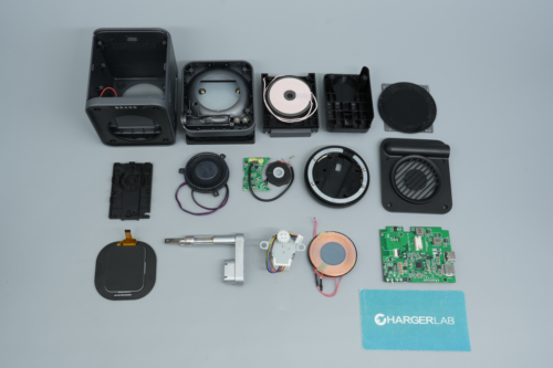
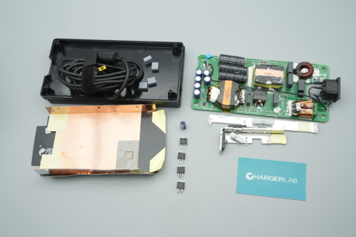
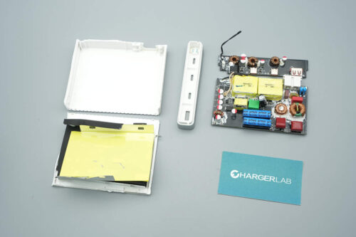
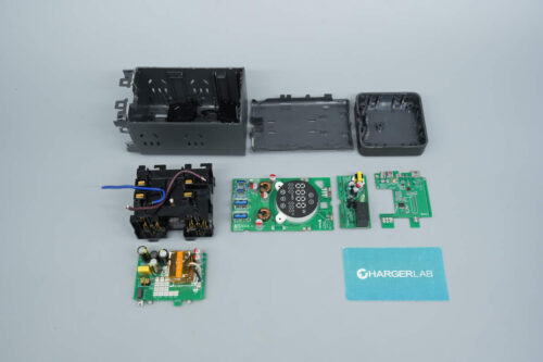
Teardown
Next, let's take it apart to see its internal components and structure.
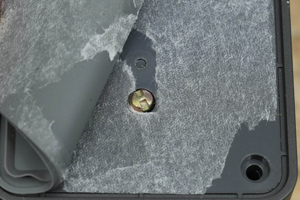
Remove the bottom foot pad; there are concealed screws inside.
Remove the screws to separate the housing; the enclosure is secured with snap-fit fasteners.
Welding of the battery cell to the PCBA module.
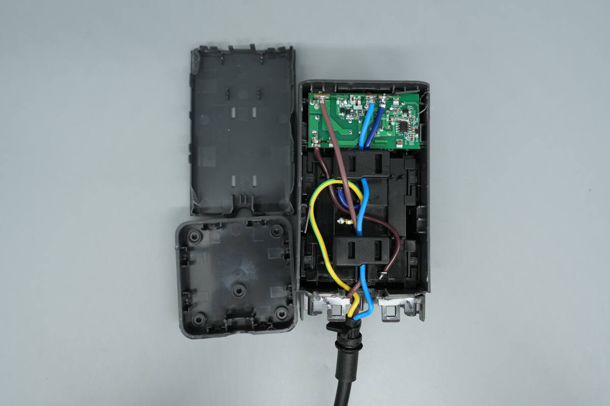
Separate the conductors of the power cord and remove the module; the AC socket module also provides support and secures the PCBA module.
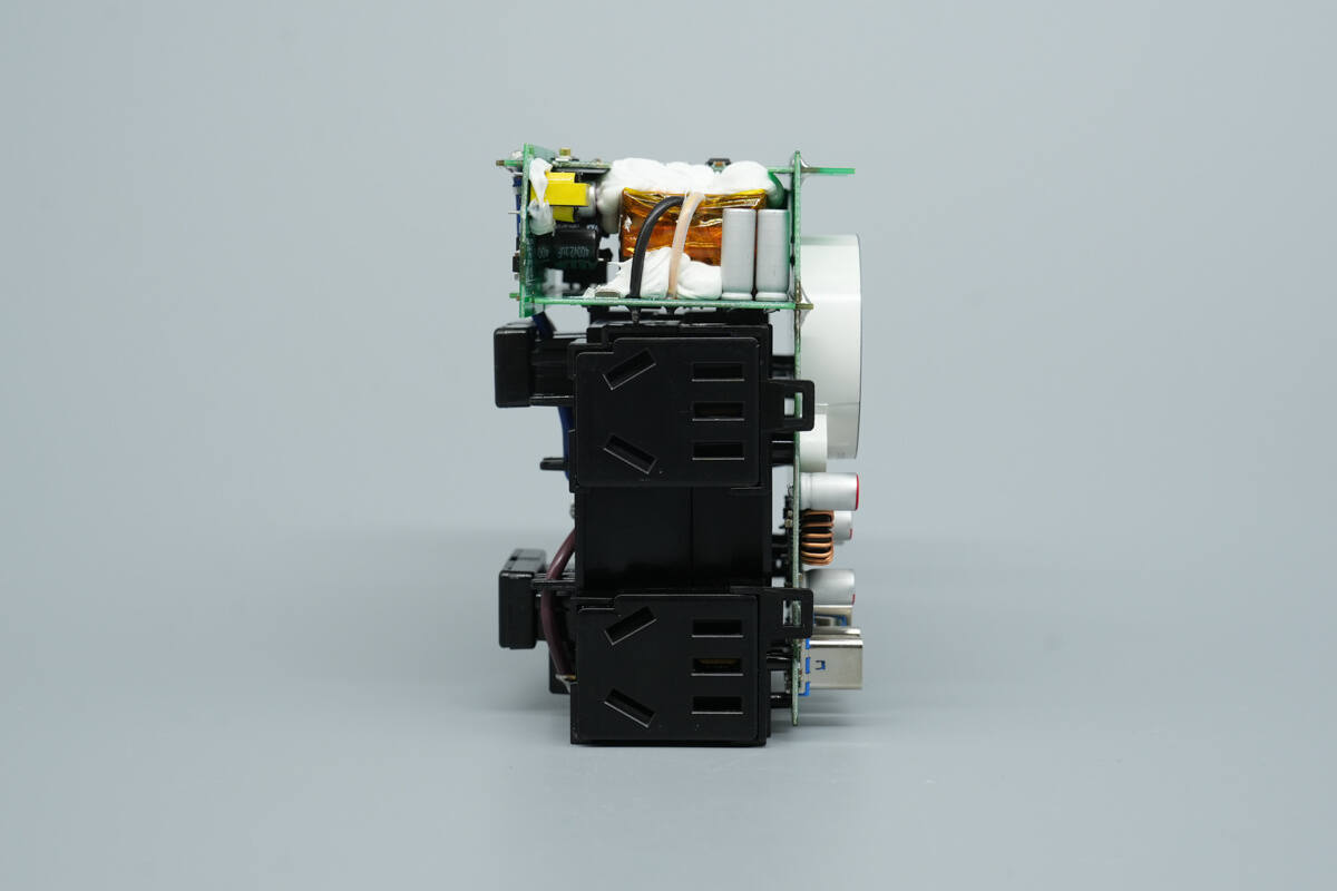
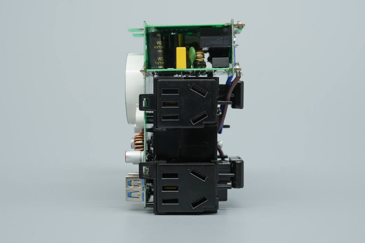
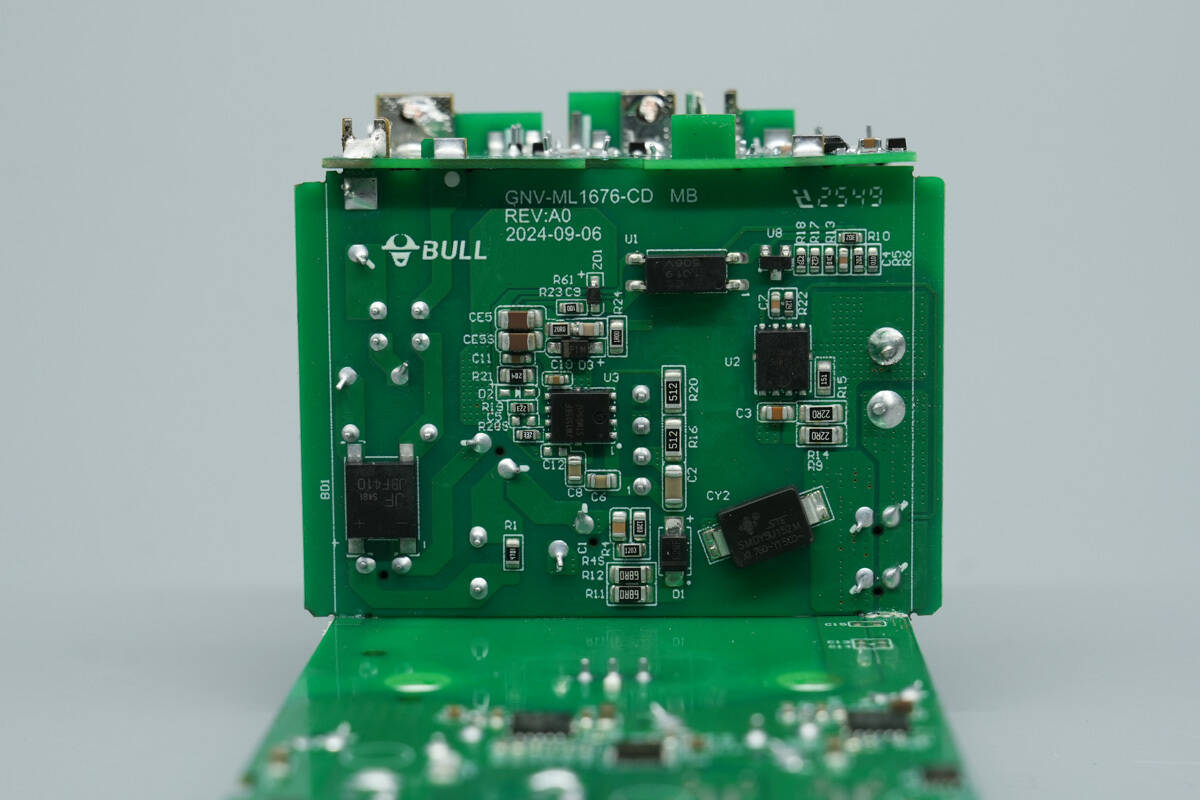
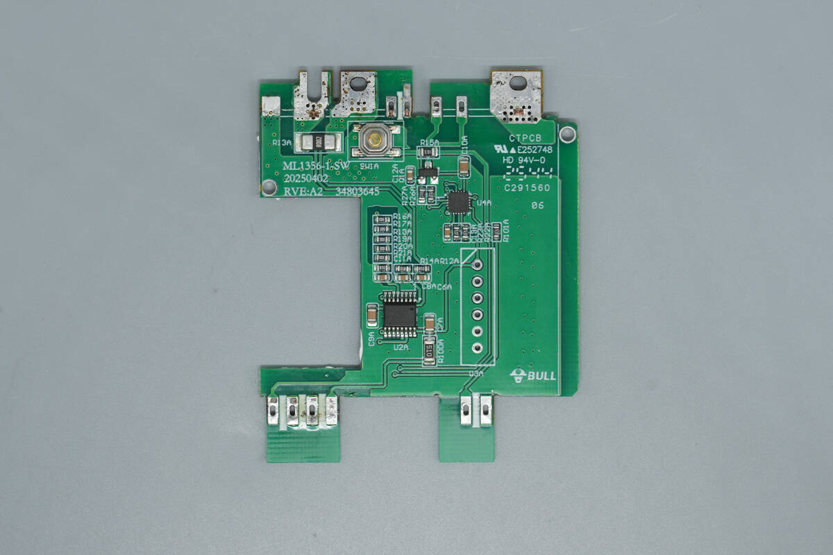
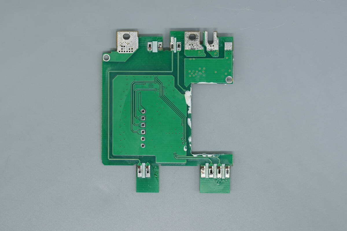
The PCBA module consists of four stacked PCBs.
Separate the AC socket module and remove the cover plate at the socket.
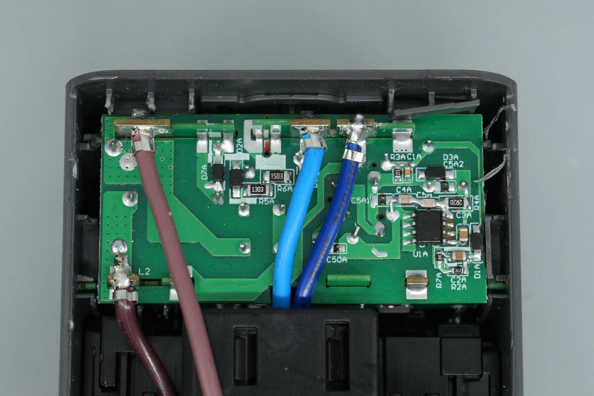
A switching power supply chip is mounted on the rear of the PCBA module.
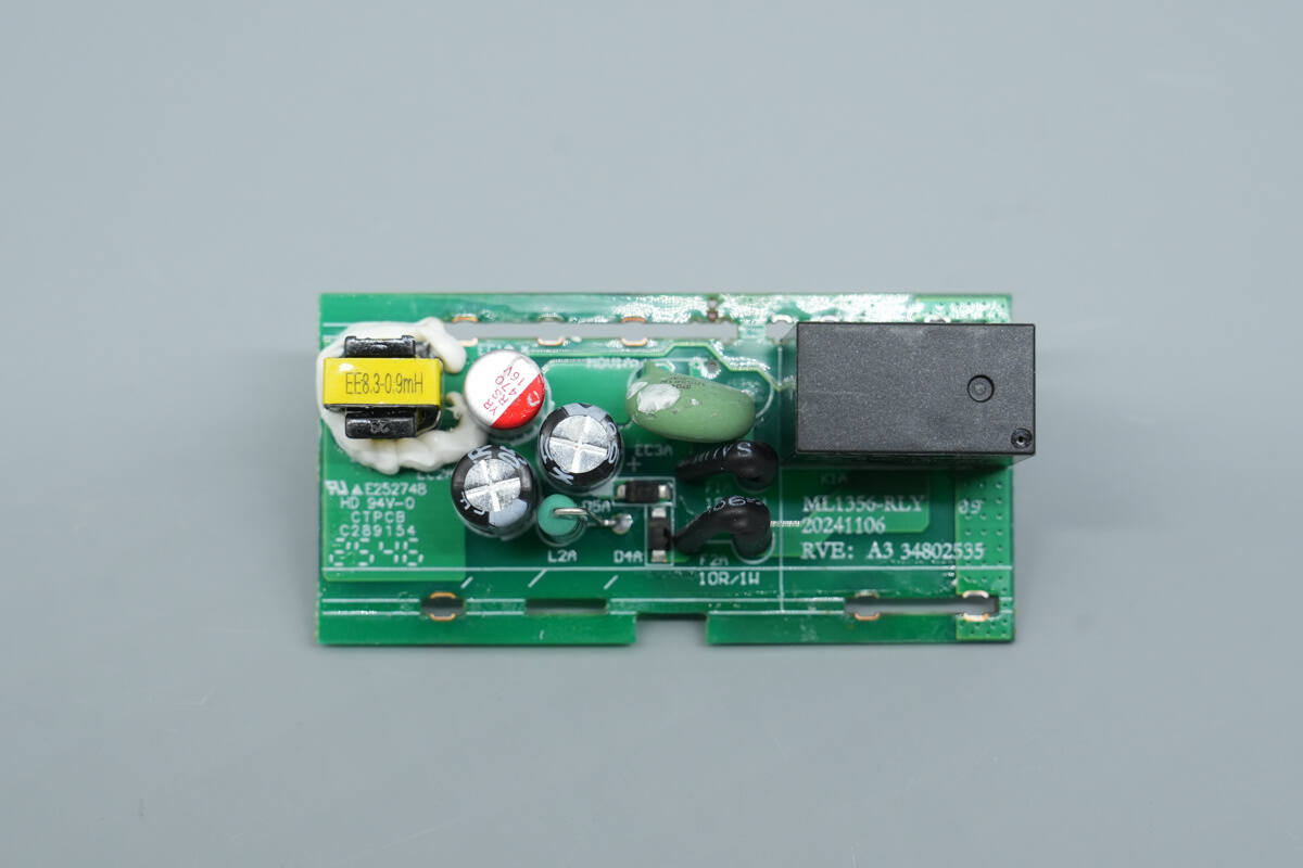
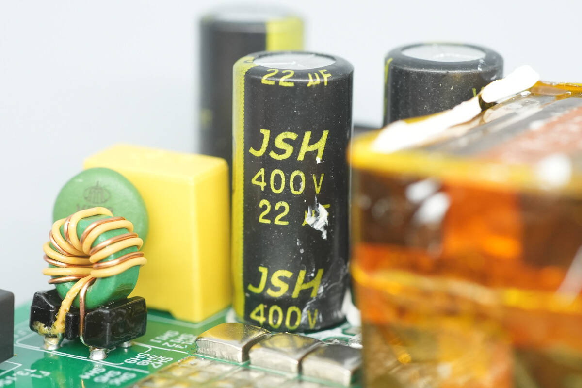
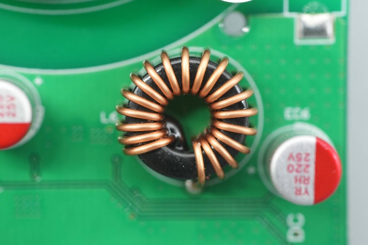
The other side houses fuses, varistors, relays, filter capacitors, transformers, and other components.
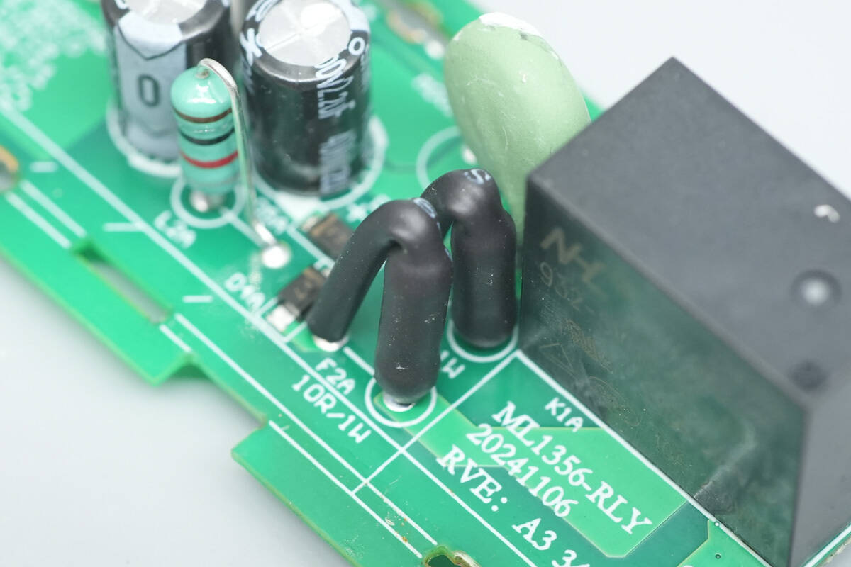
The fuse is protected by heat‑shrink tubing.
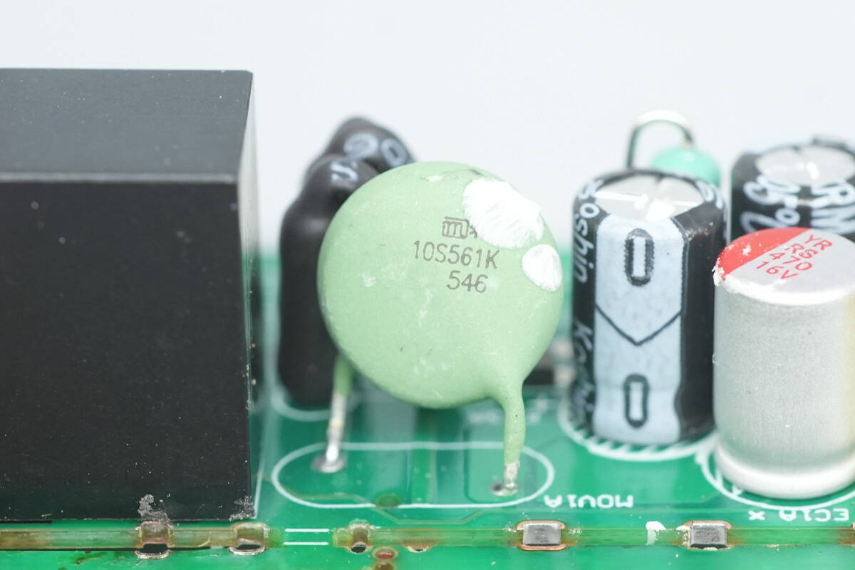
The varistor from JOYIN, model 10S561K, is used to absorb overvoltage surges.
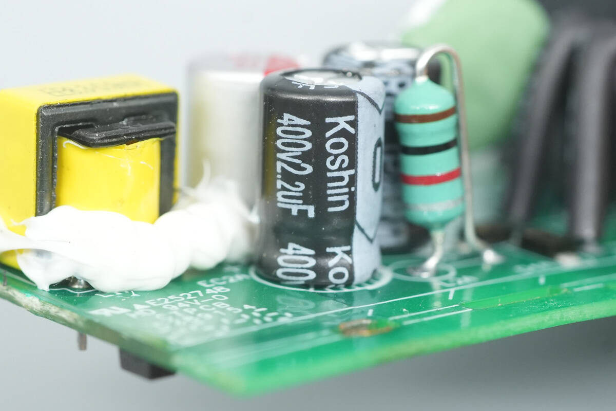
The filter capacitor from Koshin, rated 400 V and 2.2 μF.
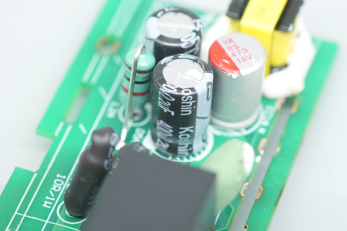
Another capacitor with the same specifications.
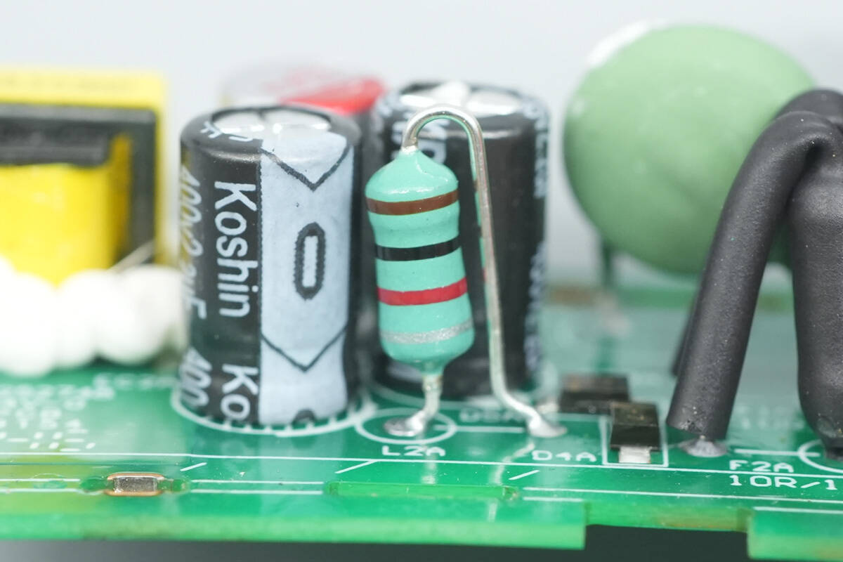
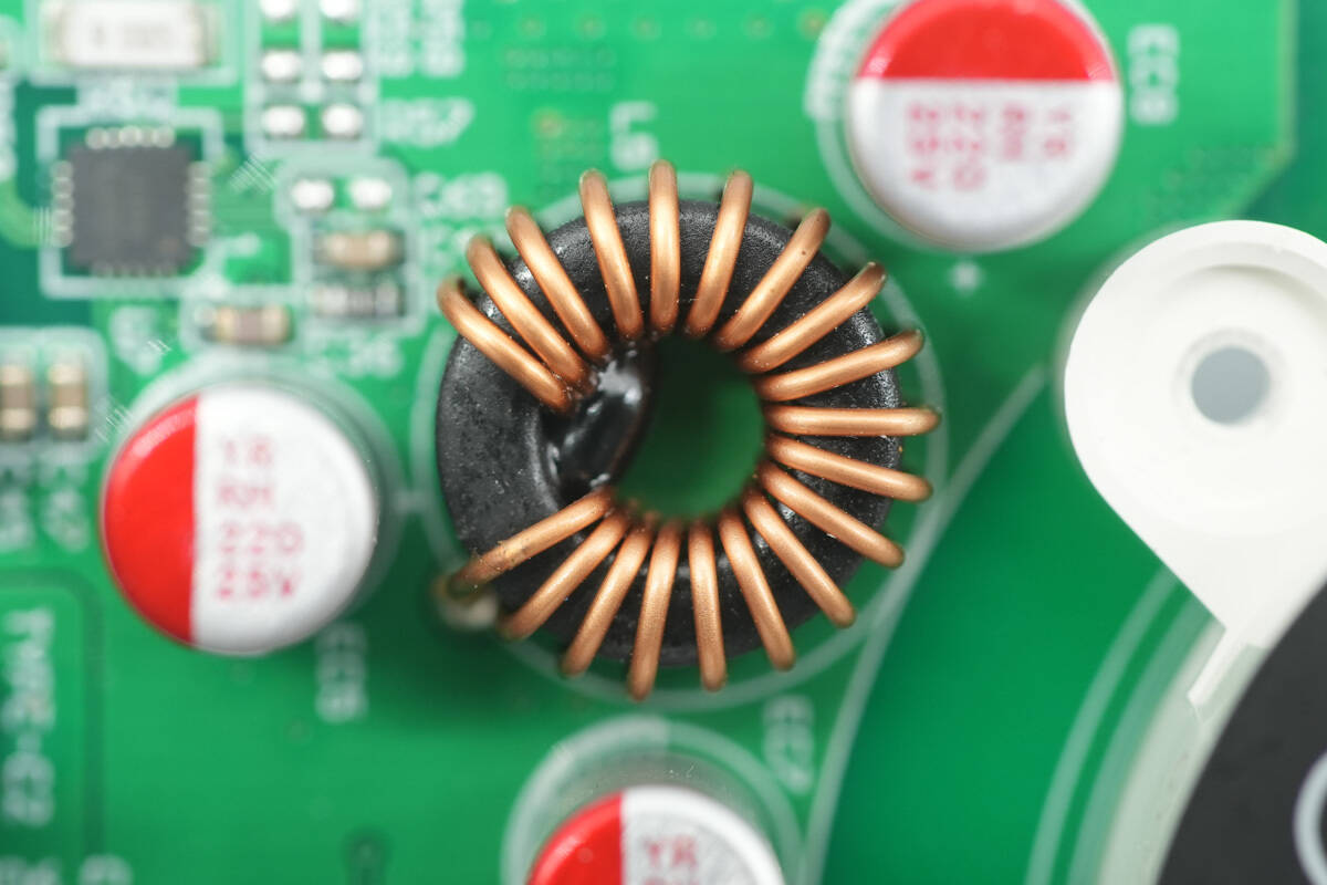
The Color-band inductor is used for filtering.
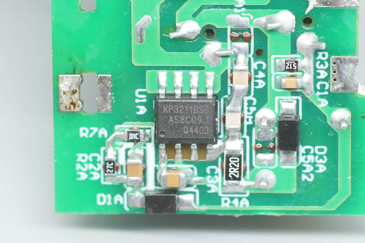
The power supply IC from Kiwi Instruments, model KP3211B. This family is a high-performance, low-cost PWM-controlled switching power supply suitable for offline, small-power buck-type applications, with simple peripheral circuitry and few components. The device also integrates a high-voltage MOSFET to improve the system's surge tolerance.

KP321XB integrates a complete set of self‑recovery protection features: VDD undervoltage protection, cycle‑by‑cycle current limiting, output overvoltage protection, overtemperature protection, overload protection, and VDD overvoltage protection.
The transformer windings are insulated with insulation tape.
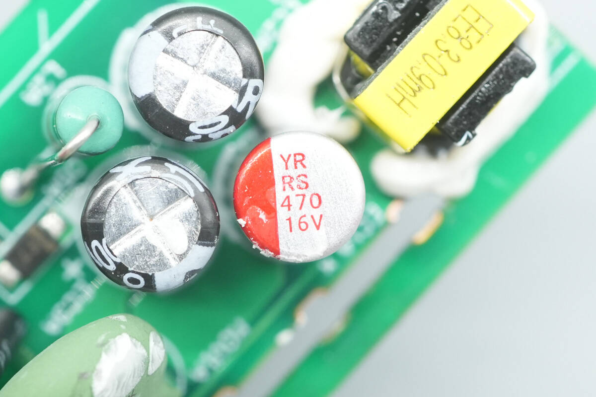
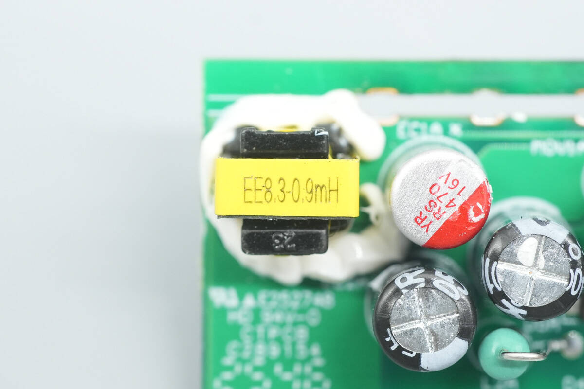
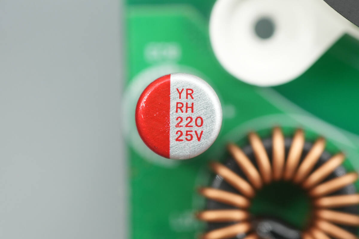
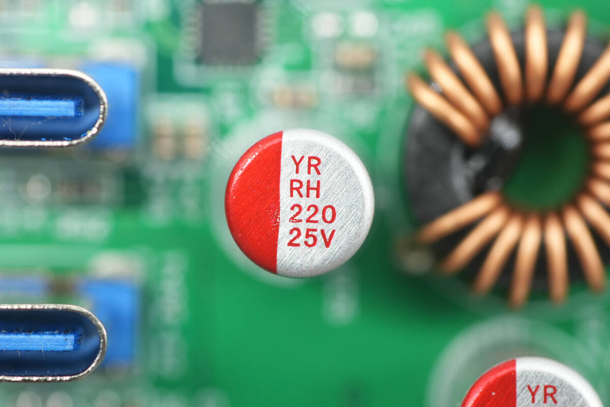
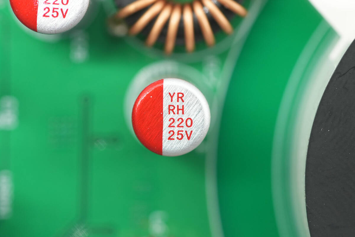
The solid-state capacitor from YUNRUI, rated 16 V and 470 μF.
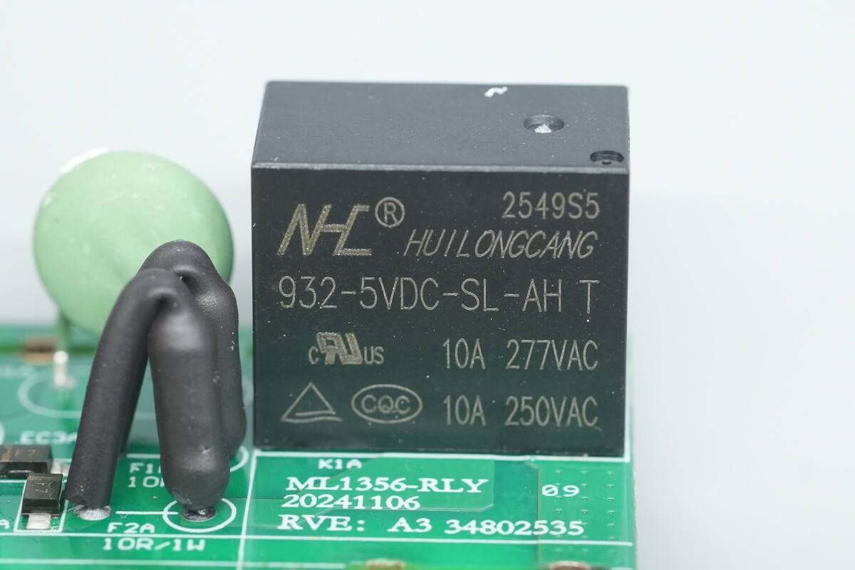
The power-control relay is from NHC, model 932-5VDC-SL-AH; a compact power relay with a 5 V coil and a contact rating of 16 A.
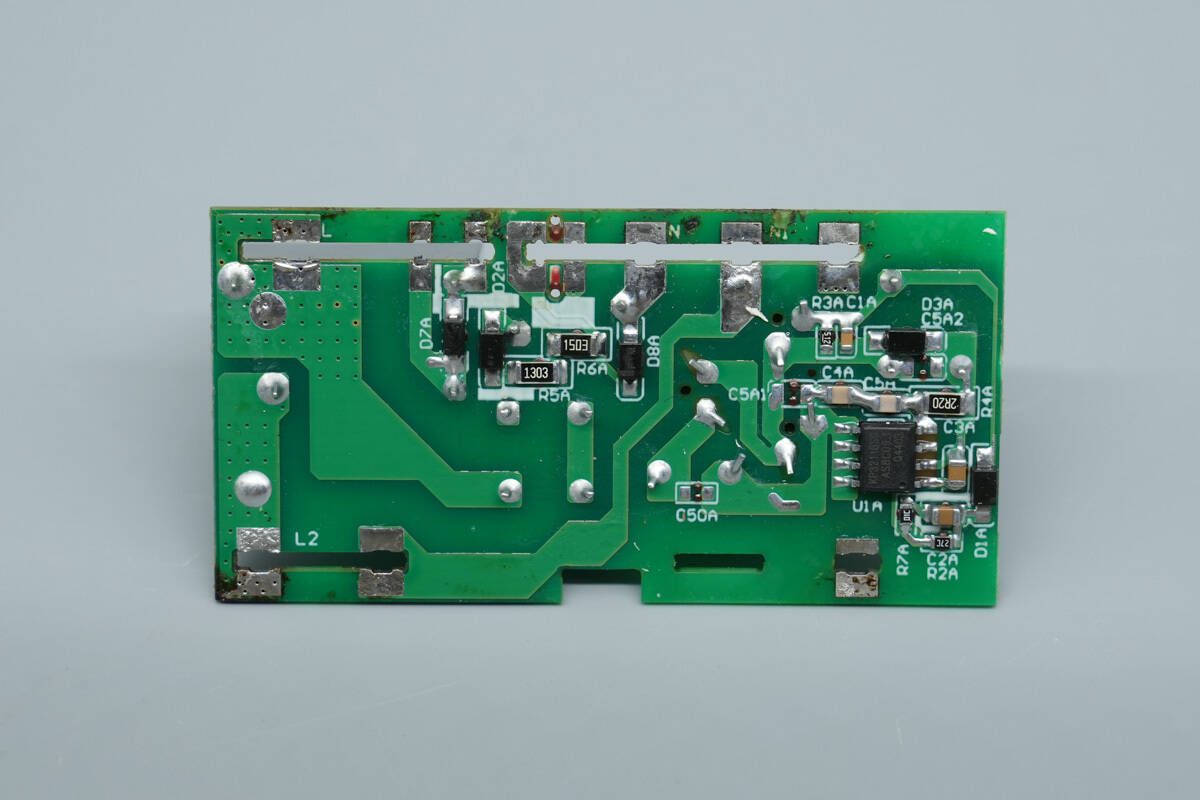
The back of the small PCB at the bottom of the module houses a bridge rectifier, the main power-management IC, an optocoupler, a Y capacitor, and a synchronous rectifier chip.
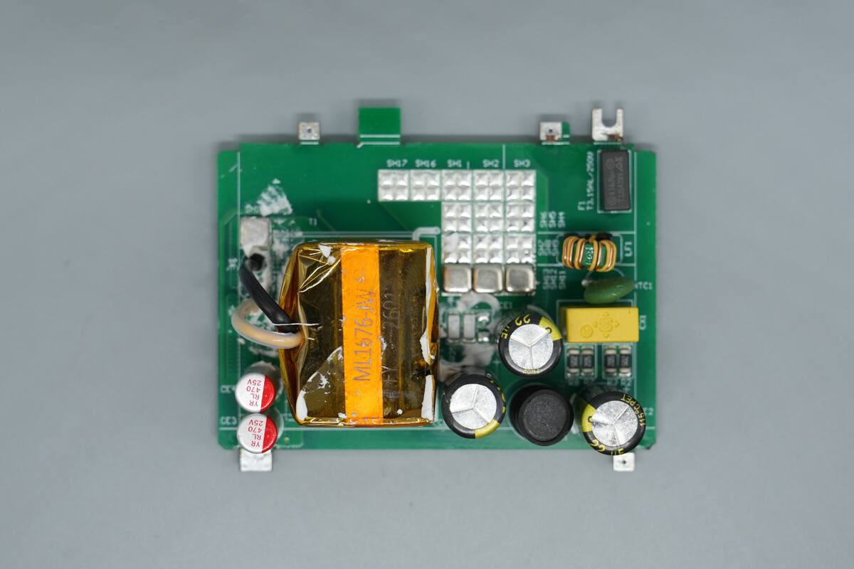
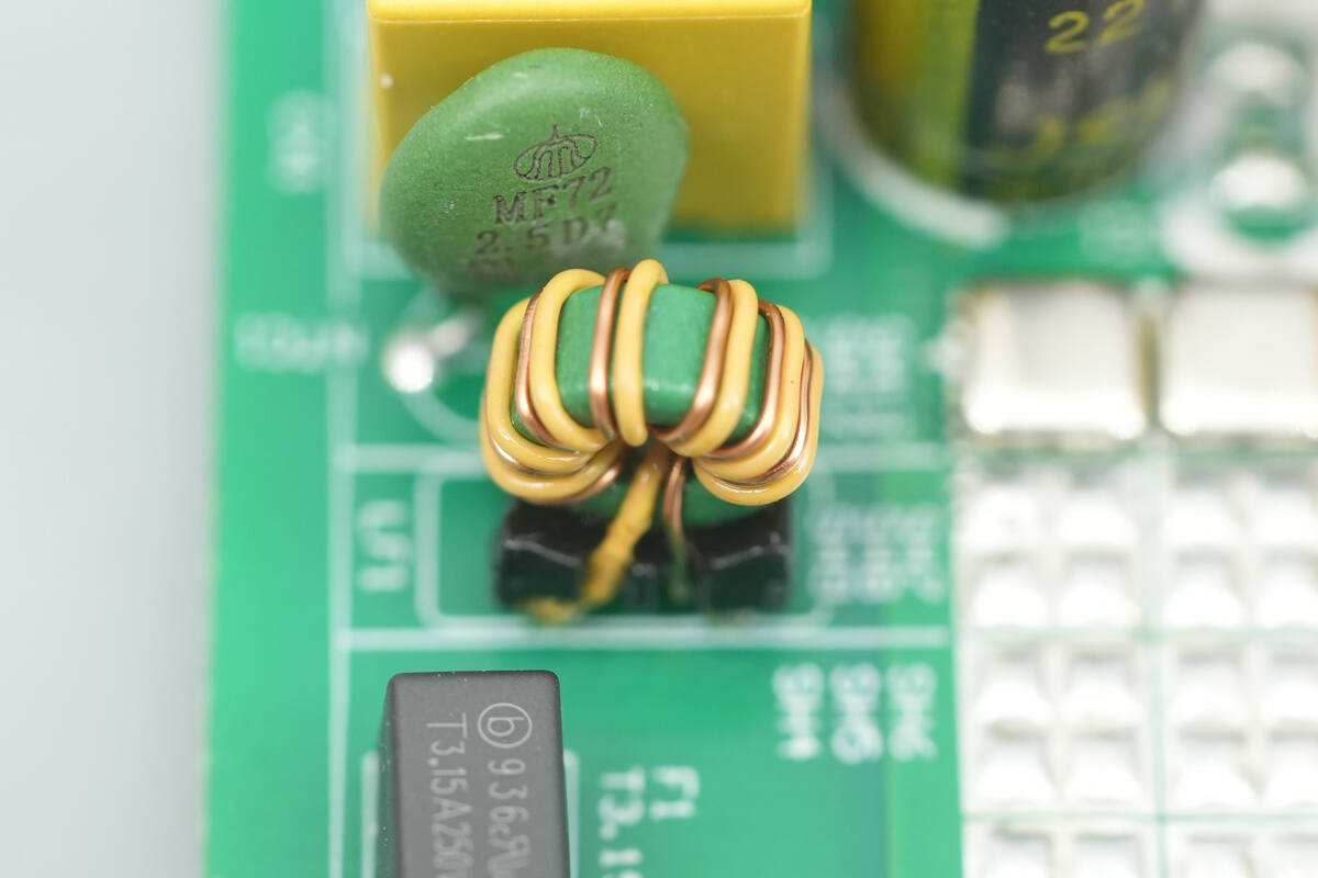
After disassembling the module, the front side of this small PCB includes a fuse, a common-mode choke, a safety X2 capacitor, an NTC thermistor, high-voltage filter capacitors, an I-shaped inductor, a transformer, and solid-state capacitors.
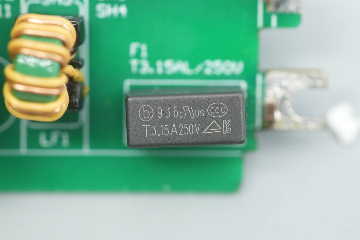
The time-delay fuse is from Betterfuse, part number 936, specification 3.15A 250V.
The common mode choke is a double-winding used to filter out EMI.

The NTC thermistor, from shiheng, is part of the MF72 series and is marked with 2.5D7. It is used to suppress surge current during power-up.
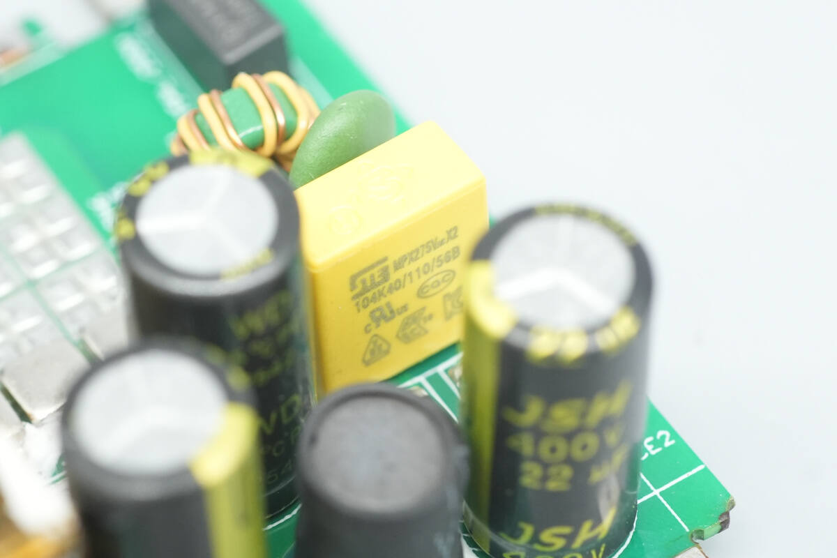
The safety X2 capacitor is from STE and has a capacitance of 0.1μF.
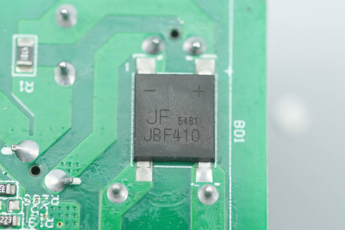
The bridge rectifier is from JF, model JBF410.
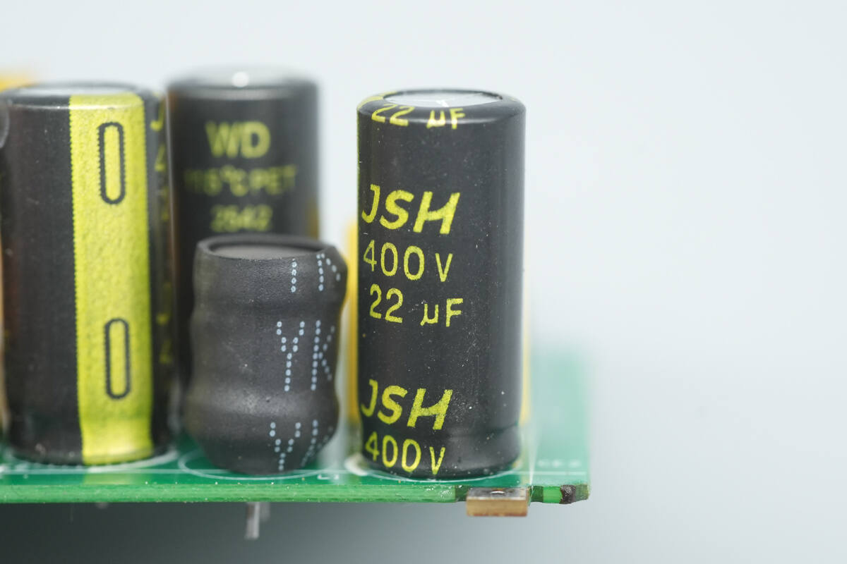
All three high-voltage filter electrolytic capacitors are from JSH, and their specifications are all 400V 22μF.
A close-up of the second capacitor.
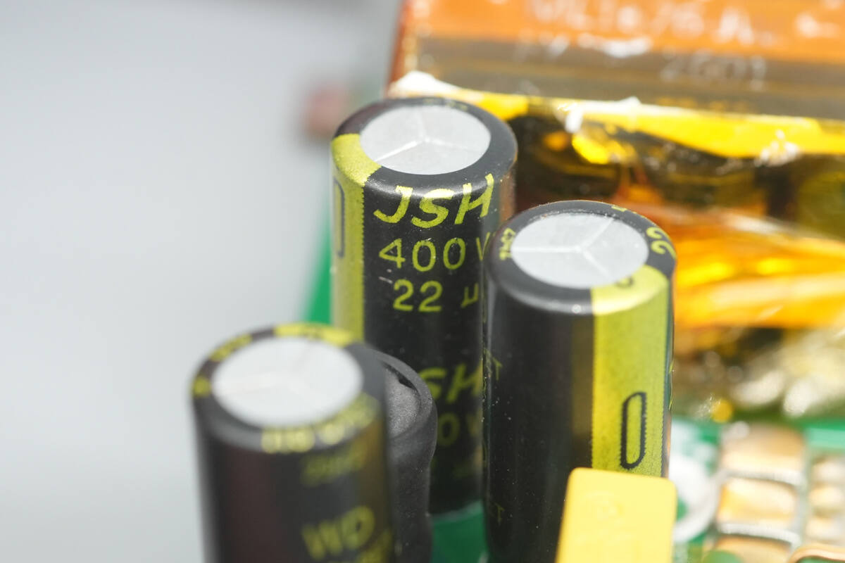
A close-up of the third capacitor.
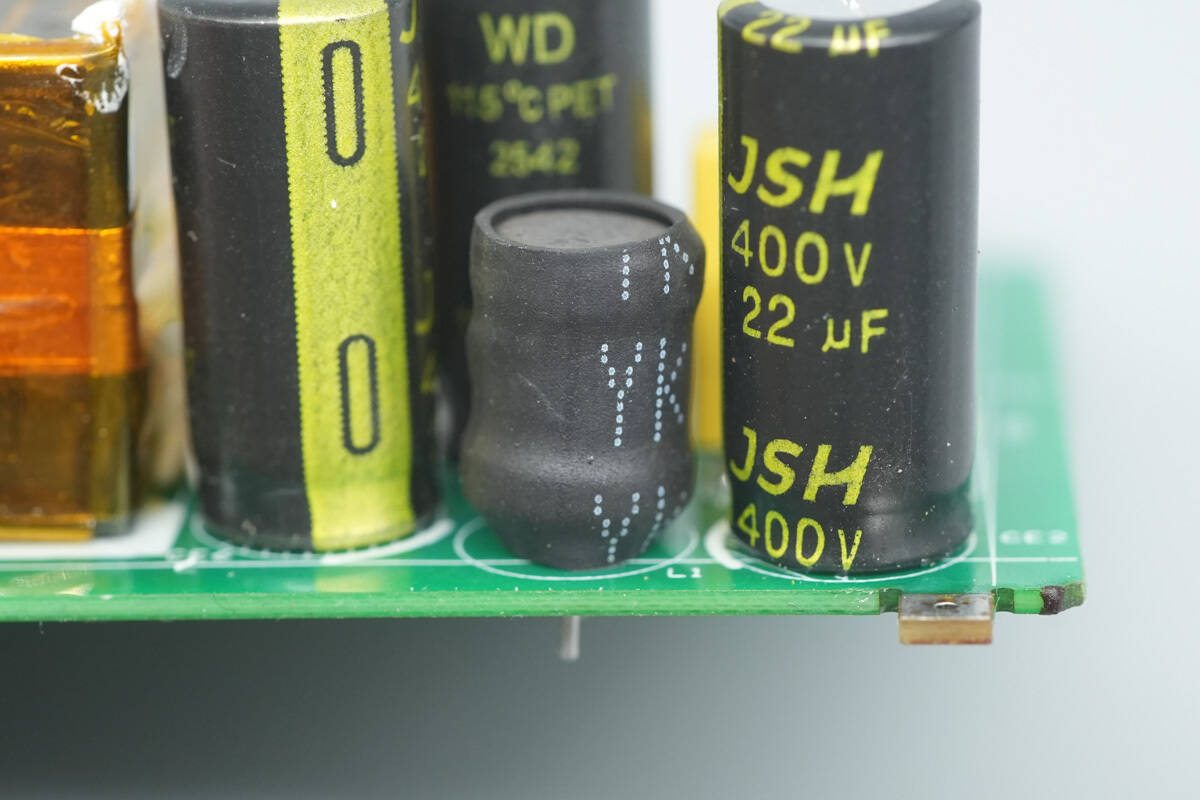
The I-shaped inductor with heat shrink tubing insulation.
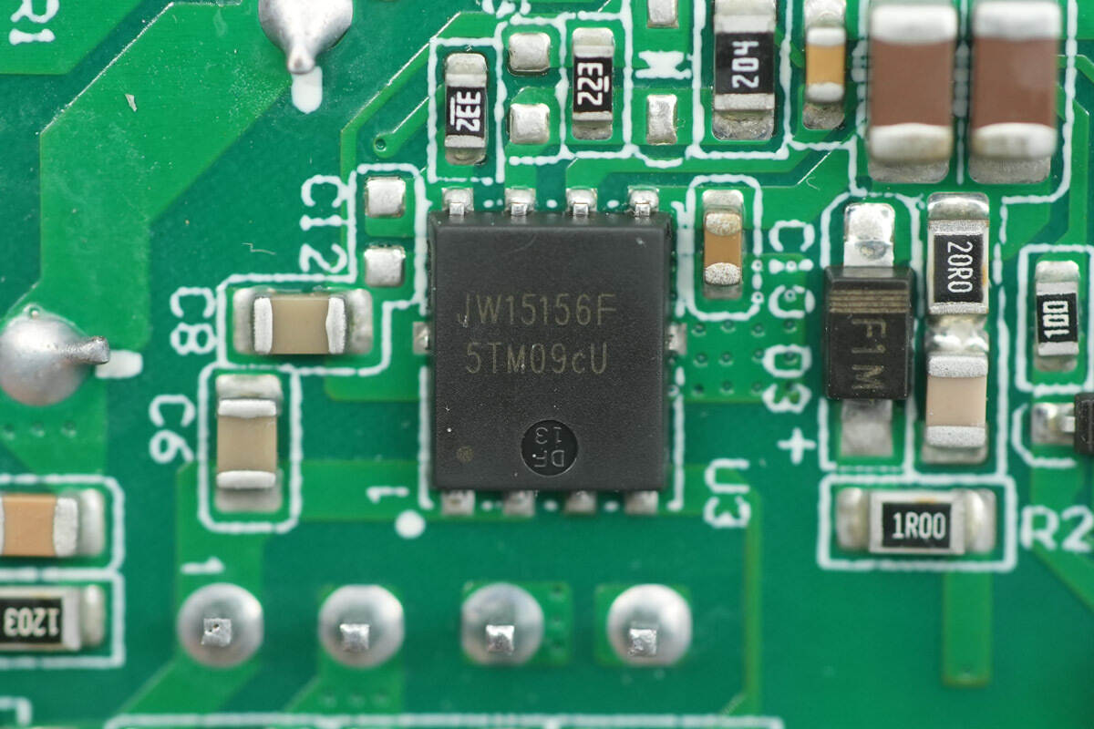
The master control chip is from JOULWATT, model JW15156F. This is an isolated offline flyback converter with integrated GaN and a QR operating mode. It improves efficiency by reducing switching losses and enhances EMI performance by utilizing its inherent frequency-varying characteristics. Simultaneously, it employs internal frequency limiting technology to overcome the inherent drawbacks of quasi-resonant flyback topologies.
The JW15156F includes a high-voltage (HV) pin for startup, eliminating the need for a traditional startup resistor and reducing power consumption in standby mode.
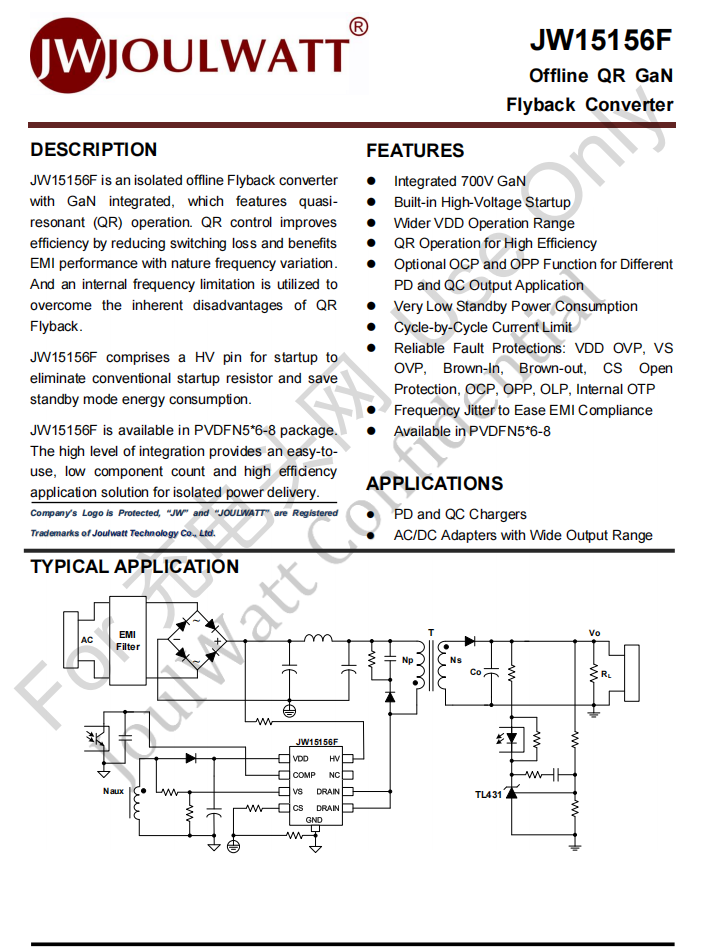
The JW15156F is packaged in a PVDFN5*6-8 package. Its high integration provides an easy-to-use, low-component-count, and high-efficiency application solution for isolated power delivery.
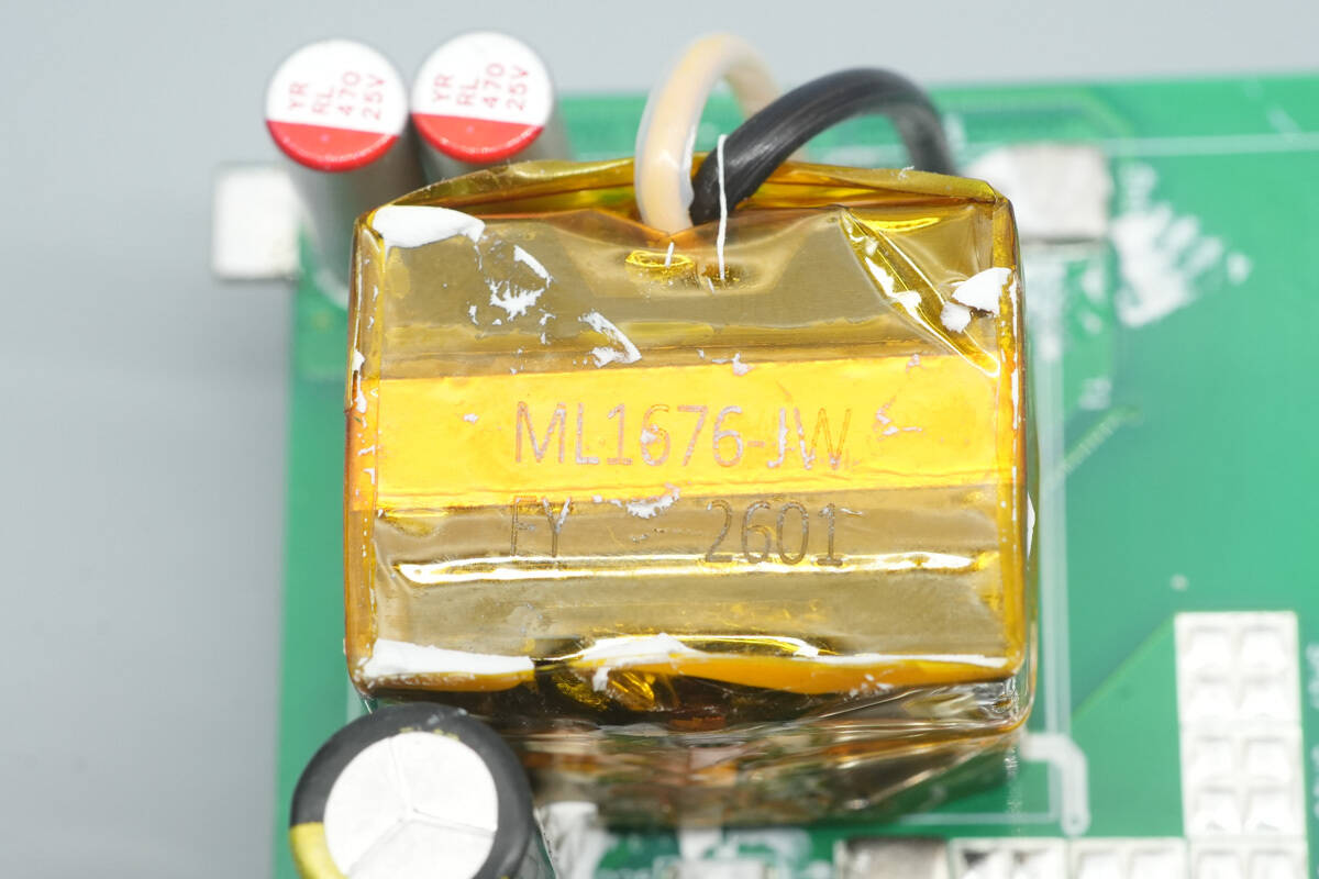
The transformer core is wrapped with high-temperature resistant insulating tape.
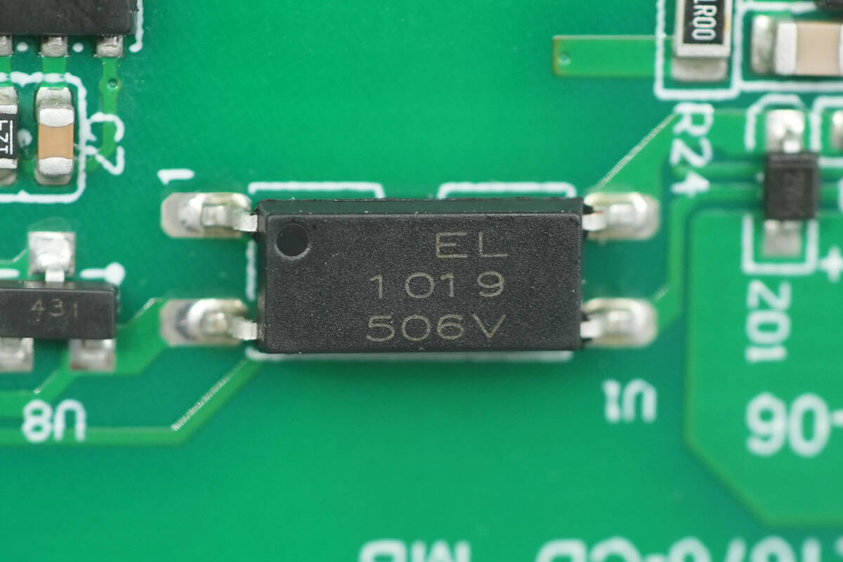
The Everlight EL1019 optocoupler is used for output voltage feedback.
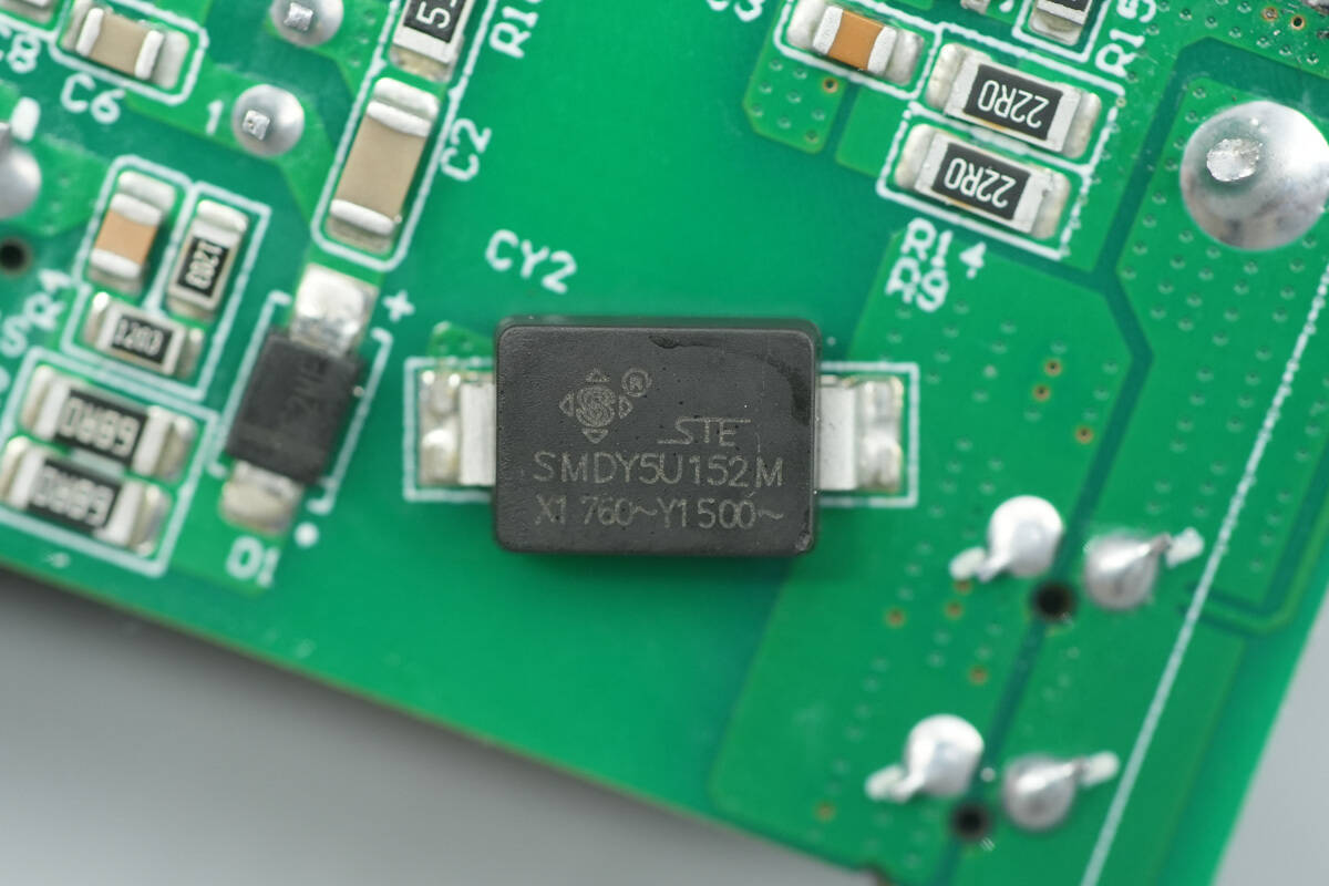
The SMD Y capacitor uses the STE SMD-X1Y1 series, model SMDY5U152M, with a height of only 2.5mm. Compared to traditional leaded capacitors, its size is significantly reduced, making it suitable for highly integrated applications.
Its tape and reel packaging design is compatible with SMT automated insertion and soldering processes, greatly improving production efficiency and driving the development of end products towards full surface mount technology and miniaturization. Furthermore, the product uses flame-retardant epoxy resin encapsulation material, meeting the UL94V-0 flame retardant rating, ensuring safety and reliability in high-temperature and high-risk environments.
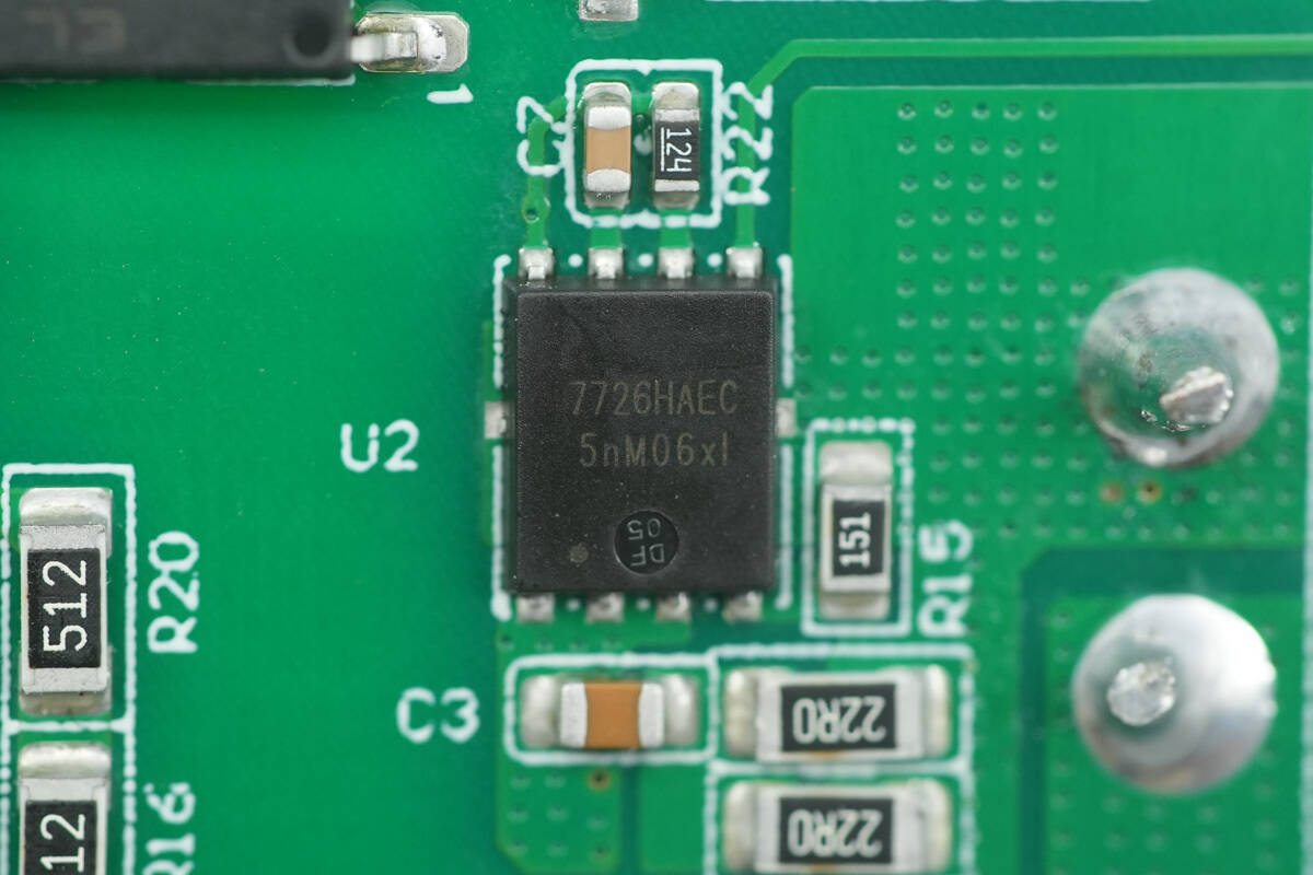
The synchronous rectifier chip, model JW7726HAEC, is from JOULWATT and is specifically designed for secondary-side rectification in isolated topologies such as active-clamped flyback, continuous/quasi-resonant/discontinuous-mode flyback.
Compared to traditional diode rectification solutions, this device significantly improves system efficiency. Furthermore, the device uses a PVDFN5*6-8 package, providing a compact solution for high-efficiency power systems.
The JW7726HAEC achieves precise control by real-time monitoring of the MOSFET's Vds voltage: the internal MOSFET is turned on when Vds is below -140mV, and immediately turned off when the voltage rises back above -6mV.
The chip supports multiple operating modes, including Discontinuous Conduction Mode (DCM), Critical Conduction Mode (CrCM), Continuous Conduction Mode (CCM), and quasi-resonant mode. It also employs JOULWATT's proprietary technology to overcome the synchronous rectification challenge in CCM mode.
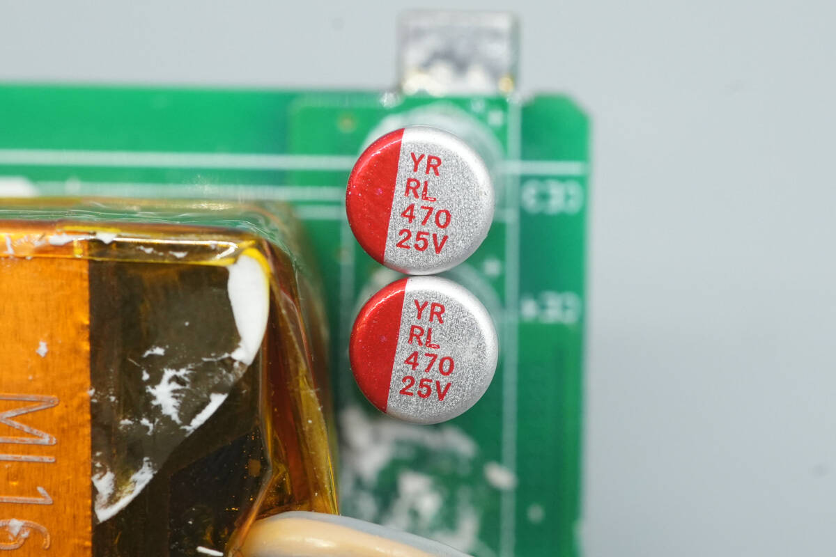
The two output solid capacitors are from YUNRUI, and both are rated at 25V 470μF.
The front of the PCB board of the module features two step-down inductors for step-down circuits, filter solid capacitors, a USB-C1 port protocol chip, and a smart digital display screen.
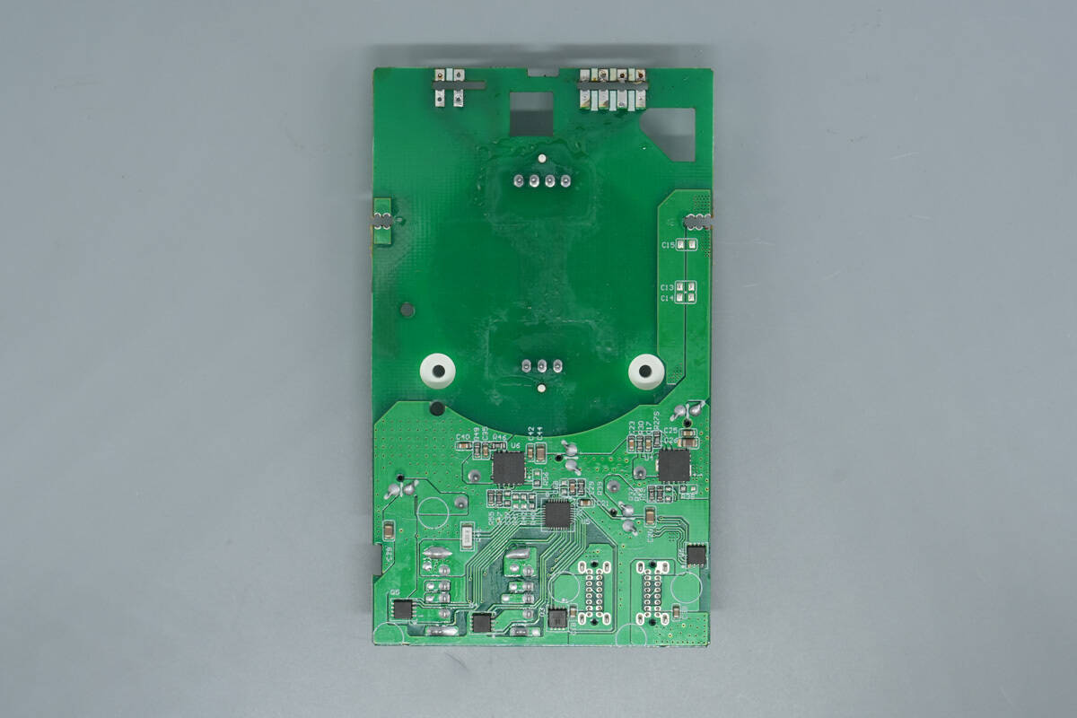
On the back are a synchronous buck converter with two buck circuits, a protocol chip, and VBUS MOSFETs.
A power metering chip is located on the front of the small PCB at the top of the module.
The other side has no components.
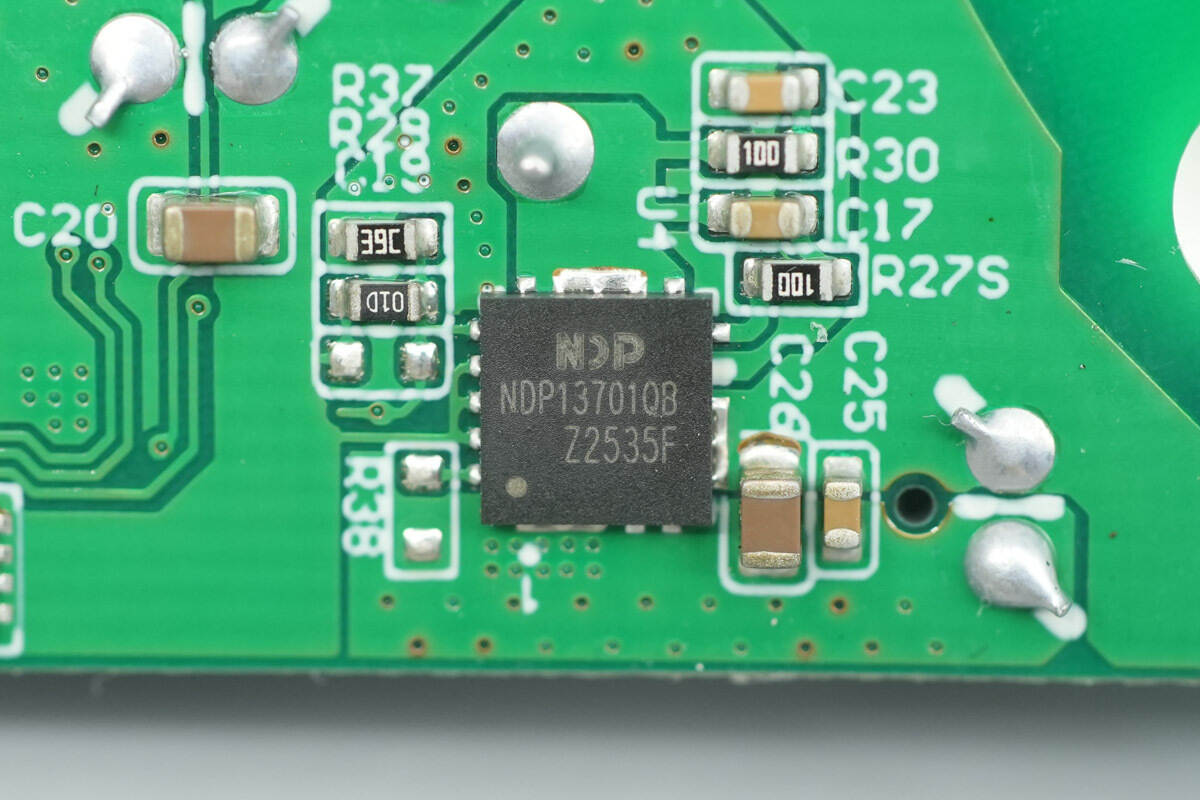
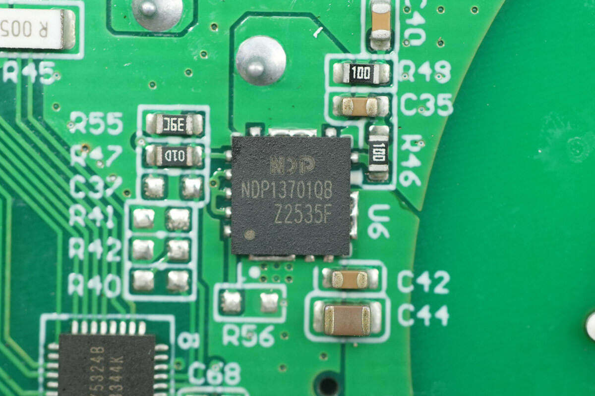
The synchronous buck converter for the USB-C1 port is from NDP, model NDP13701QB. It supports 7-30V input voltage and 7A output current, integrates MOSFET, supports dual constant voltage and constant current control, integrates internal loop compensation, and uses a QFN5*5 package.
Close-up of a step-down inductor.
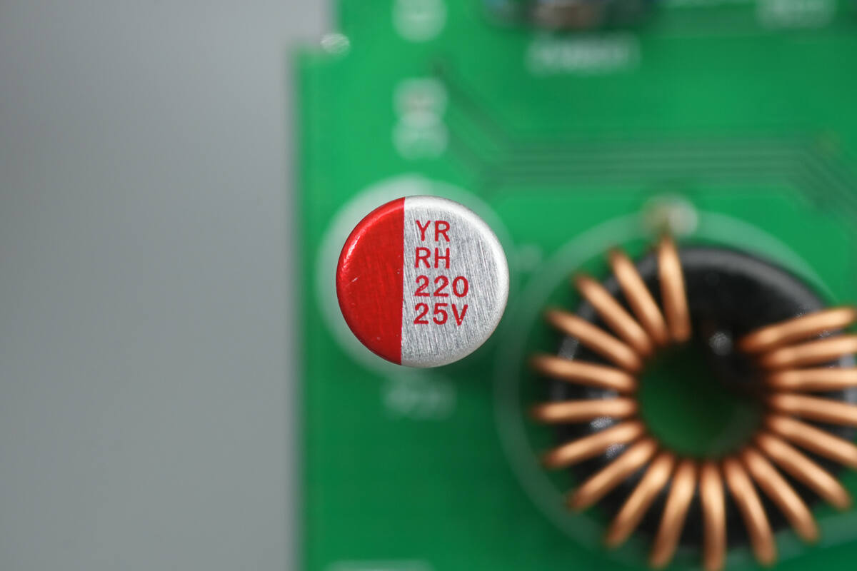
The solid capacitors are from YUNRUI and are rated at 25V 220μF.
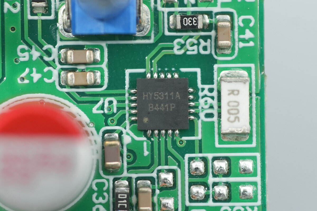
The USB-C1 port protocol chip is from HYASiC, model HY5311. This is a high-performance, highly integrated USB Type-C power delivery port controller. The device fully complies with the USB Power Delivery Specification Revision 3.1 (version 1.8) and supports seven programmable current and voltage PDOs.
The HY5311 also supports BC1.2DCP, Apple2.4A, QC2.0/3.0/3.0+, AFC, FCP, SCP, and PE+1.1/2.0 protocols. It integrates Power-Link technology for easy implementation of multi-port applications. It also supports external I2C and enables intelligent power distribution.
The HY5311 incorporates comprehensive protection mechanisms, including overvoltage protection, undervoltage lockout, overcurrent protection, output short-circuit protection, CC or DPDM overvoltage protection, and overtemperature protection. It is packaged in a QFN3*3-20L package.
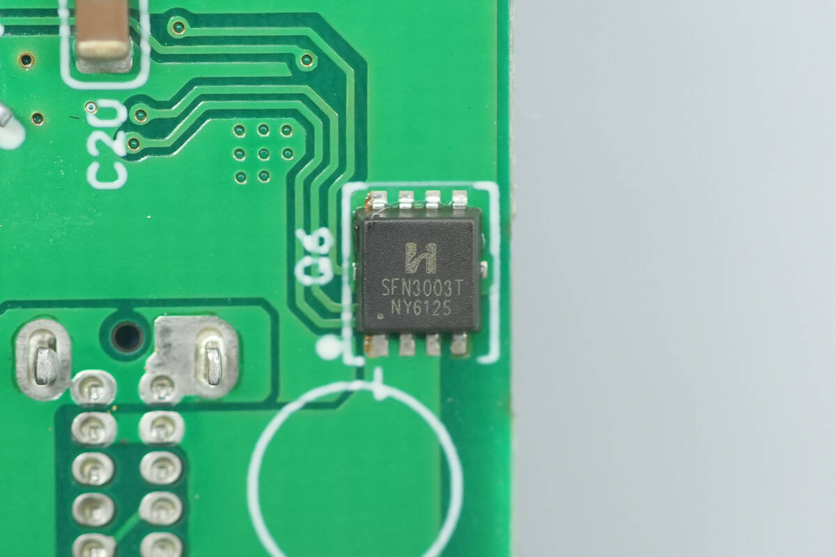
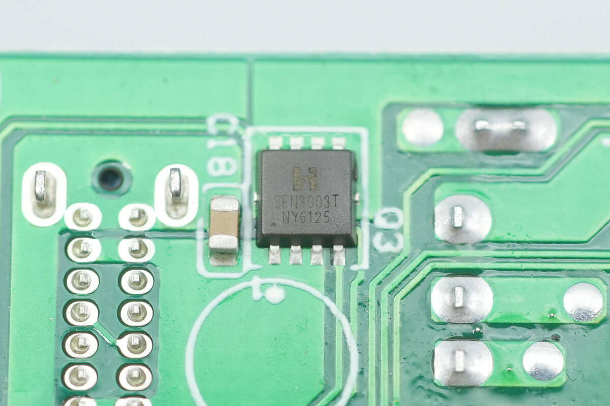
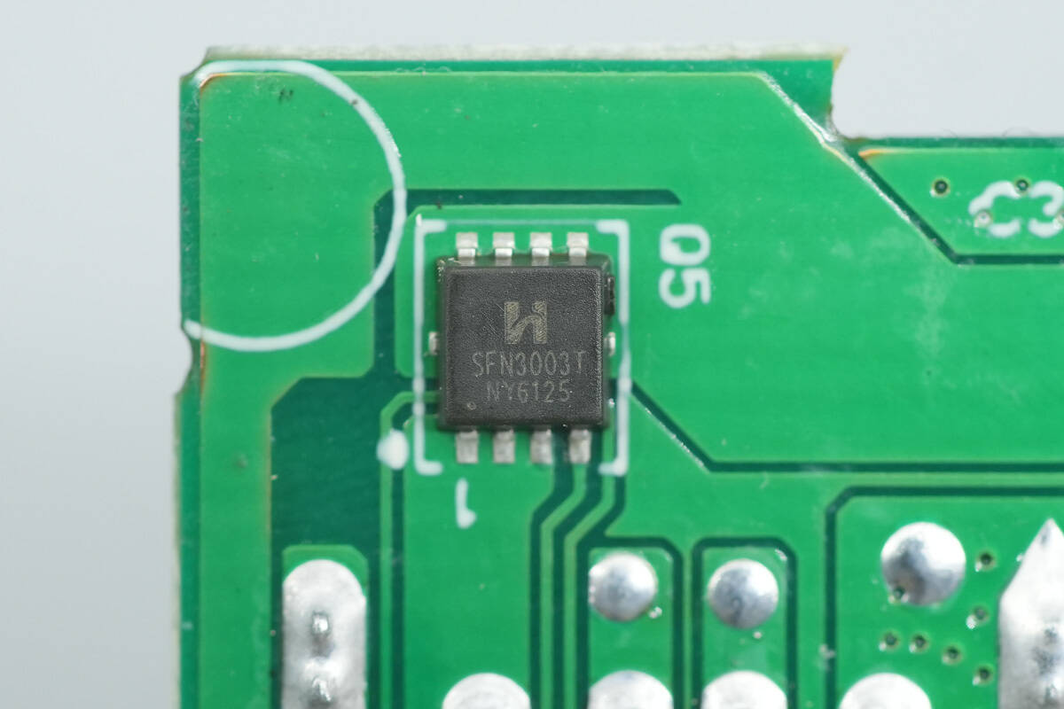
The output VBUS MOSFET of the USB-C1 port is from HI-SEMICON, model SFN3003T. It is a 30V NMOS with an on-resistance of 7.5mΩ and uses a PDFN3*3 package.
The synchronous buck converter for the other step-down circuit also uses the NDP13701QB.
Close-up of a step-down inductor.
The solid capacitors are also from YUNRUI, with a specification of 25V 220μF.
The other one has the same part number.
The third part number is the same.
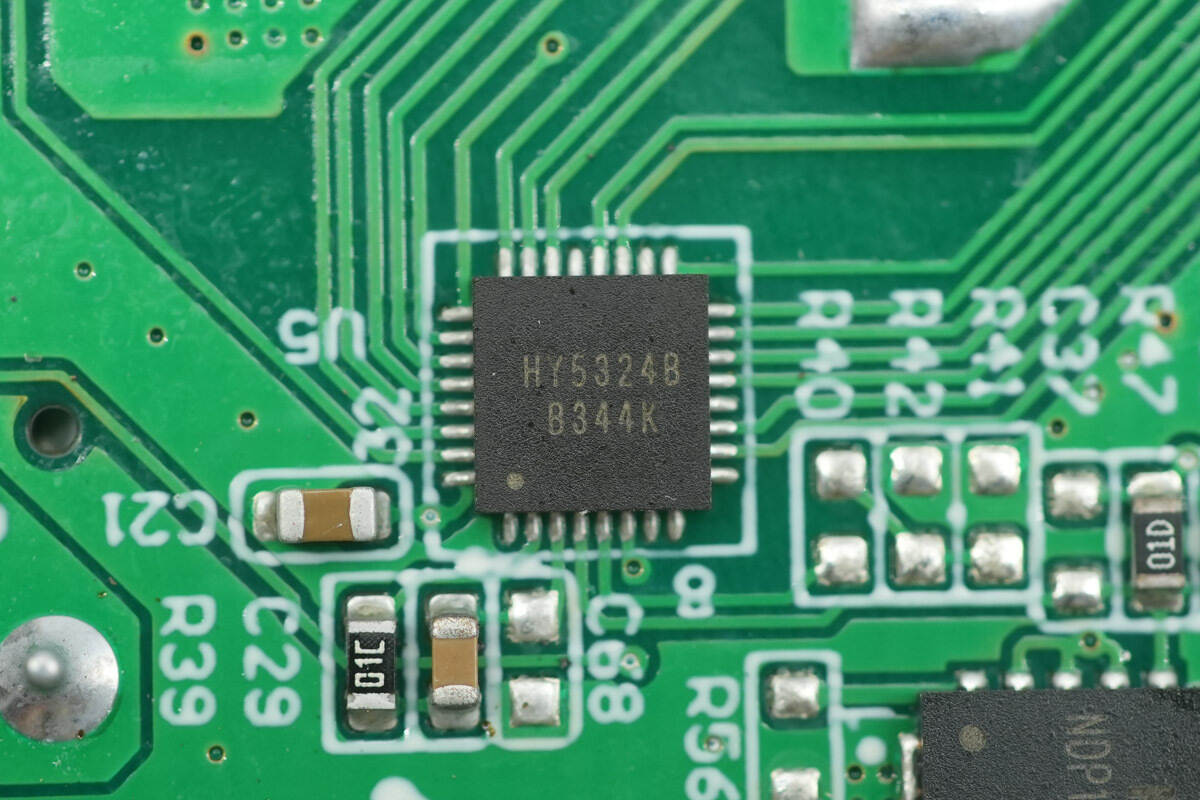
The protocol chips for the other three interface is also from HYASiC, model HY5324B. This is a high-performance, highly integrated USB Type-C power delivery and Type-A multi-port controller, supporting BC1.2DCP, Apple 2.4A, QC2.0/3.0/3.0+, AFC, FCP, SCP, UFCS, and PE+1.1/2.0 protocols.
The HY5324B is designed specifically for multi-port controllers and can be easily applied to 1C2A solutions. Each port operates independently in fast charging mode, and power is shared when two or more ports are working simultaneously.
The HY5324B integrates Power-Link technology, easily enabling multi-port power-sharing applications. The chip has built-in comprehensive protection mechanisms, including overvoltage protection, undervoltage lockout, overcurrent protection, output short-circuit protection, CC or DPDM overvoltage protection, and overtemperature protection. The chip uses a QFN4*4-32L package.
The output VBUS MOSFET of the USB-C2 port also uses HI-SEMICON SFN3003T.
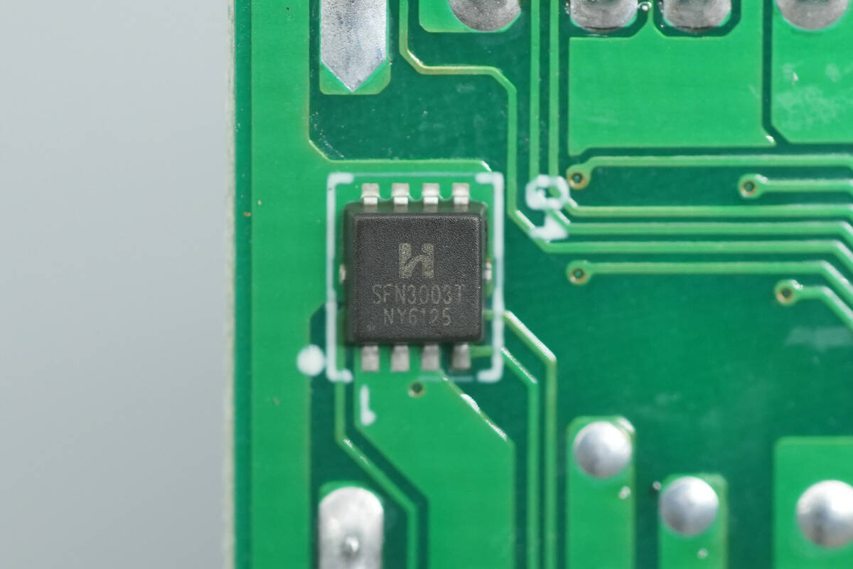
The output VBUS MOSFET of the USB-A1 port also uses HI-SEMICON SFN3003T.
The output VBUS MOSFET of the USB-A2 port also uses HI-SEMICON SFN3003T.
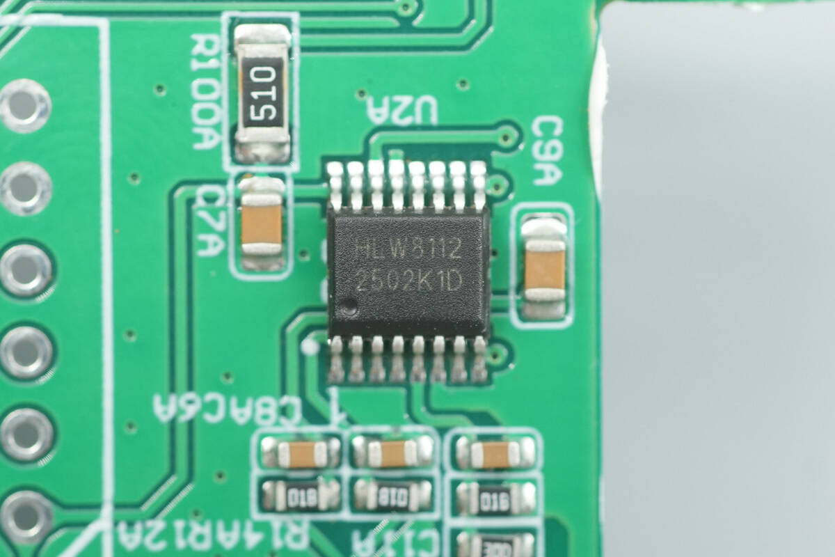
The power metering chip is model HLW8112. It is a high-precision chip that supports operating voltages of 3.3V and 5.0V. It has a built-in high-precision ADC for acquiring current signals and AC voltage from current transformers, and can also measure line frequency and calculate power factor. It is packaged in SSOP16.
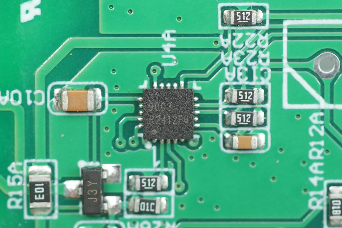
An MCU marked with 9003.
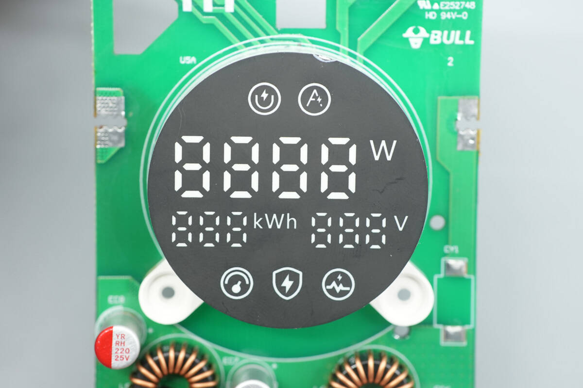
Close-up of the screen.

Well, those are all components of the BULL 67W GaN Digital Display Power Strip.
Summary of ChargerLAB
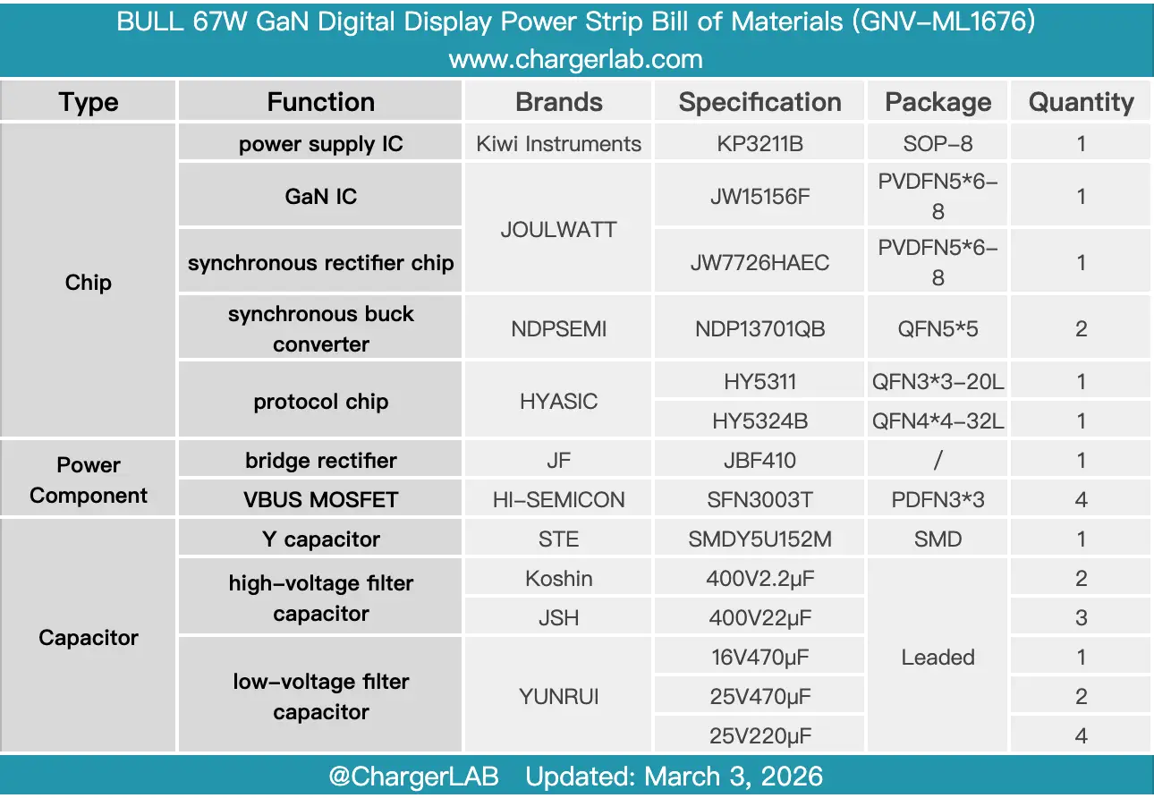
Here is the component list of the BULL 67W GaN Digital Display Power Strip for your convenience.
It is equipped with two USB-C ports and two USB-A ports, supports multiple fast charging protocols such as PD3.0 and PPS, and also features a digital display screen that can monitor power consumption in real time.
After taking it apart, we found that its USB fast charging module uses a highly integrated, encapsulated GaN power supply solution, consisting of a JOULWATT JW15156F and a JW7726HAEC chip. The secondary step-down section uses an NDP NDP13701QB paired with HYASiC HY5311 and HY5324B protocol chips.
Overall, while ensuring safety and reliability, it incorporates innovative elements such as an intelligent digital display, multi-port fast charging, and vertical design, balancing practicality and a sense of technology. It is a desktop power solution that combines quality and user experience.
Related Articles:
1. Teardown of KOAKUMA 3-in-1 Display Qi2.2 Wireless Charger
2. Teardown of Lenovo Legion 300W Original Adapter (ADL300SDC3A)
3. Teardown of MOVESPEED 165W GaN Desktop Charger (MSA05)