Introduction
Recently, we obtained the Baseus PicoGo AH11 140W GaN Fast Charger. It features a display that enables real-time visualization of charging power, power distribution, and thermal status. It also pioneers an intelligent charging summary function, allowing users to easily track charging duration and peak power output. The charger is equipped with three USB-C ports and one USB-A port, and supports 140W PD 3.1 fast charging.
Built on a GaN power solution and combined with Baseus’ self-developed BCT thermal control system, the product achieves a more compact form factor while maintaining stable power output and sustained heat dissipation. Below, we take a closer look at this Baseus charger in detail.
Product Appearance
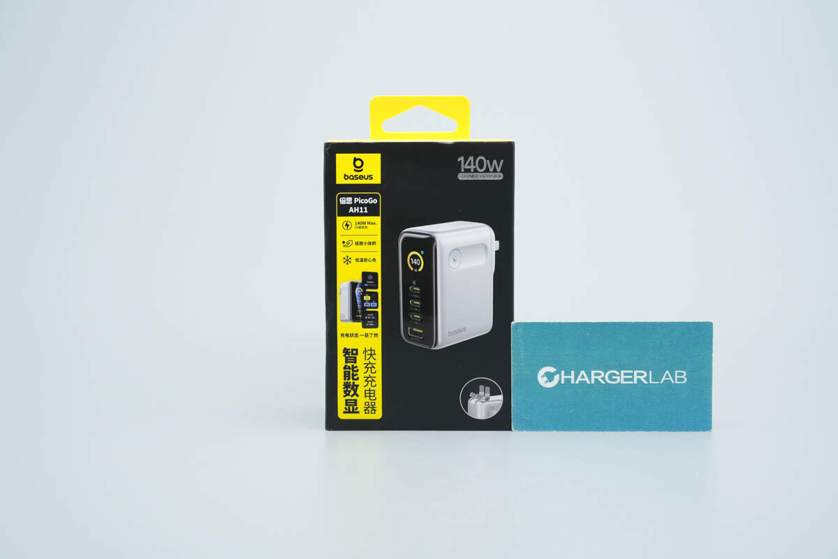
The front of the packaging box features the Baseus branding, product name, product appearance, and key selling points.
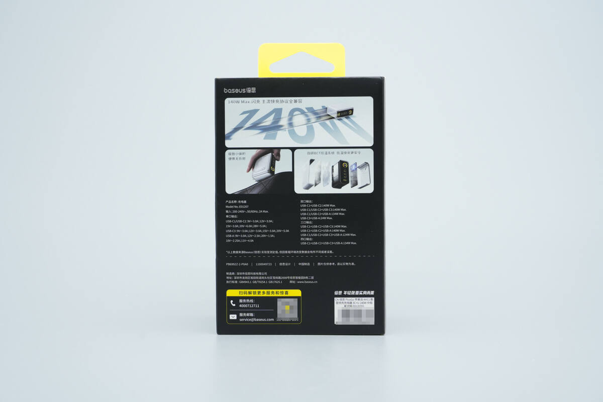
The back of the packaging displays technical specifications and other relevant information.
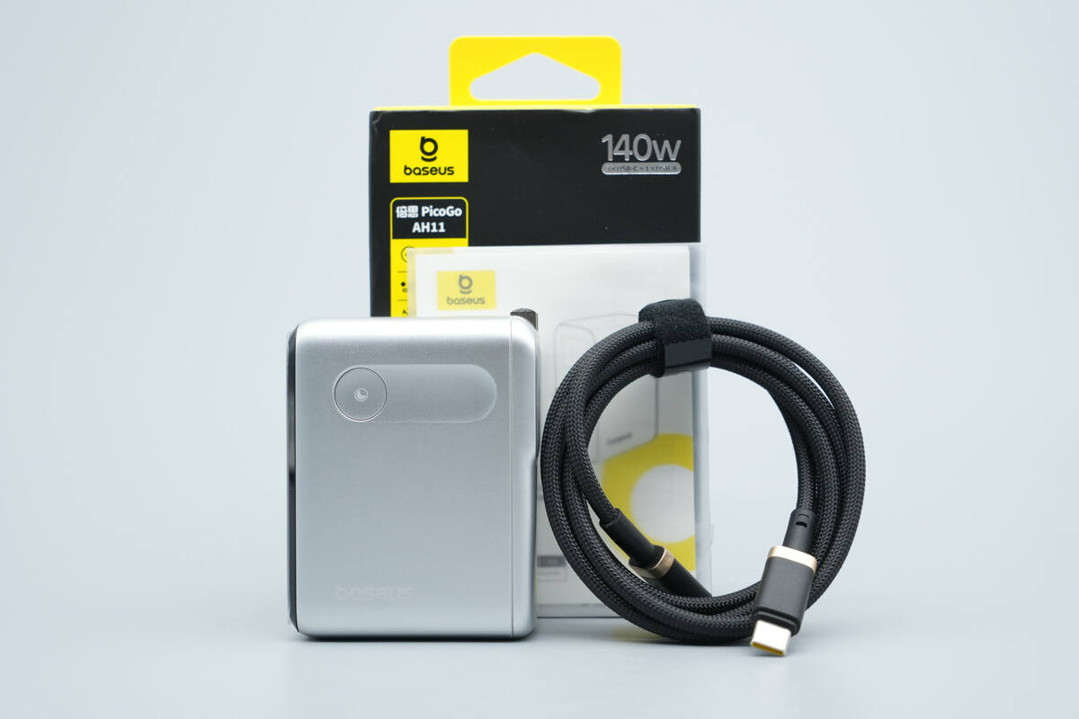
Inside the package are the charger, a charging cable, and a user manual.
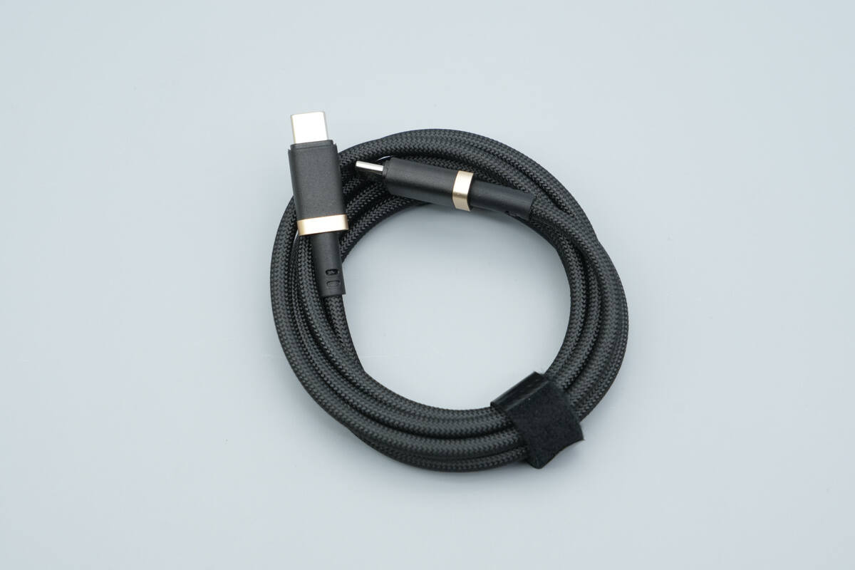
The included cable is a dual USB-C braided cable.
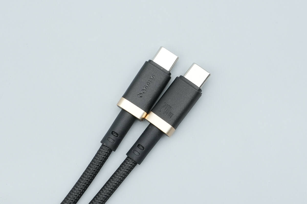
The connector housings feature a matte finish, with “Baseus” and “240W” printed on the front and back, and a metal decorative ring at the end.
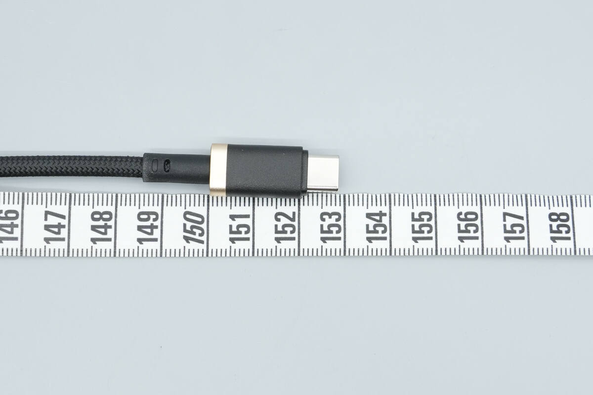
The length of the cable is about 153 cm (60.24 inches).
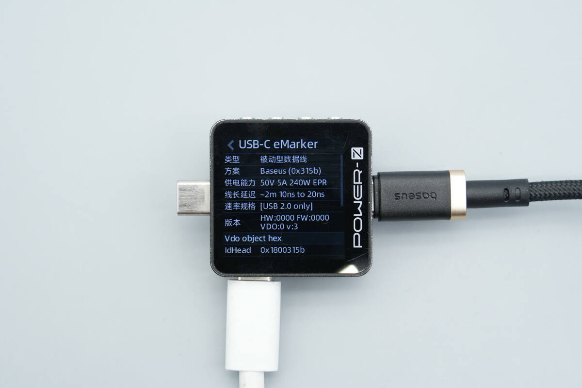
ChargerLAB POWER-Z KM003C shows that the cable is equipped with an E-Marker chip, supporting a power transmission capability of 50V 5A and a data transfer capability of USB 2.0.
The enclosure is made of flame-retardant PC material. The main body features a silver-gray finish, while the output end is finished in black.
Both sides feature ergonomically designed grooves to facilitate plugging and unplugging.

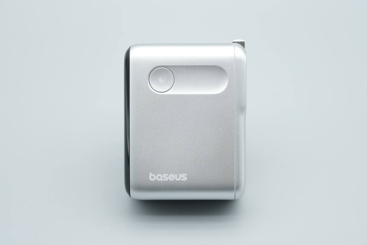
The groove on this side houses a function button, which is used to control screen off, interface switching, and angle adjustment.
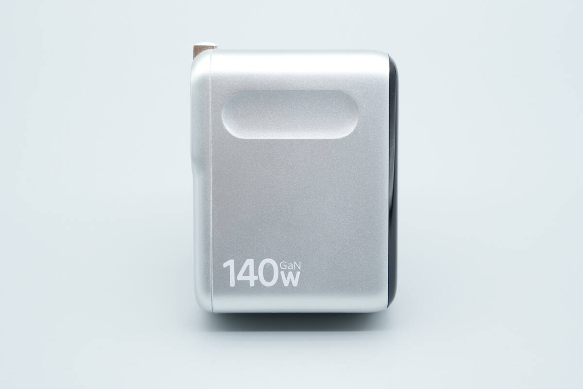
The opposite side is marked with "140W GaN".
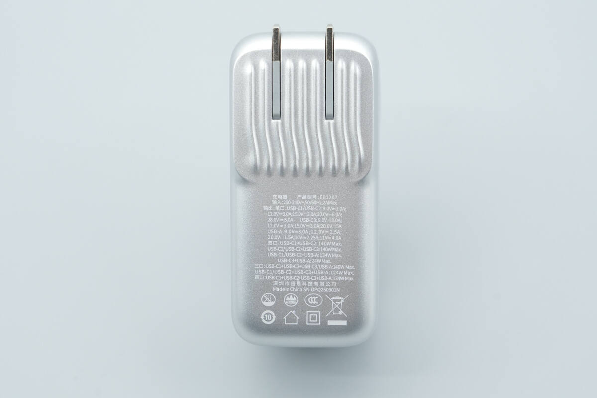
The input connector housing is printed with the technical specifications.
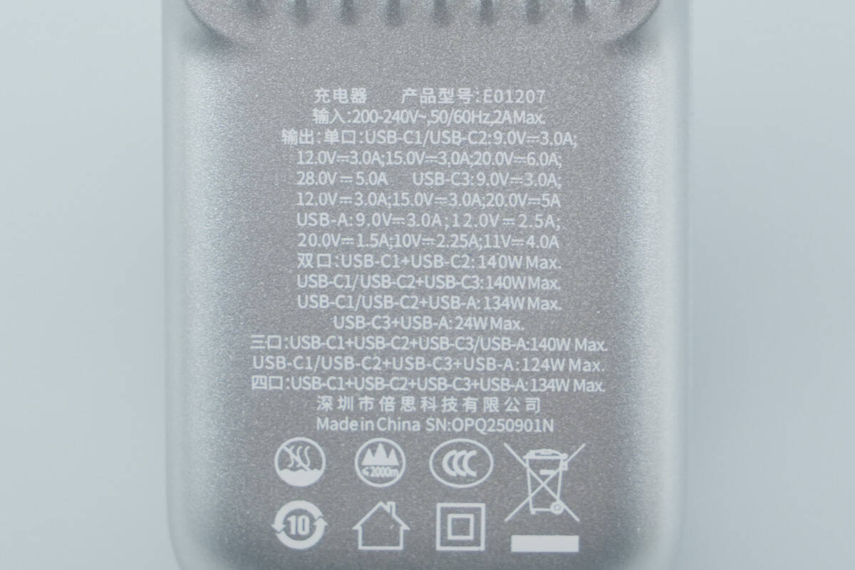
Product Model: E01207
Input: 200-240V~50/60Hz 2A Max
Single-Port Output:
USB-C1/C2: 9V 3A, 12V 3A, 15V 3A, 20V 6A, 28V 5A
USB-C3: 9V 3A, 12V 3A, 15V 3A, 20V 5A
USB-A: 9V 3A, 12V 2.5A, 20V 1.5A, 10V 2.25A, 11V 4A
Dual-Port Output:
USB-C1 + USB-C2: 140W Max
USB-C1/C2 + USB-C3: 140W Max
USB-C1/C2 + USB-A: 134W Max
USB-C3 + USB-A: 24W Max
Triple-Port Output:
USB-C1 + USB-C2 + USB-C3/USB-A: 140W Max
USB-C1/C2 + USB-C3 + USB-A: 124W Max
Four-Port Output:
USB-C1 + USB-C2 + USB-C3 + USB-A: 134W Max
The product is CCC certified.

The charger features foldable prongs for portability.
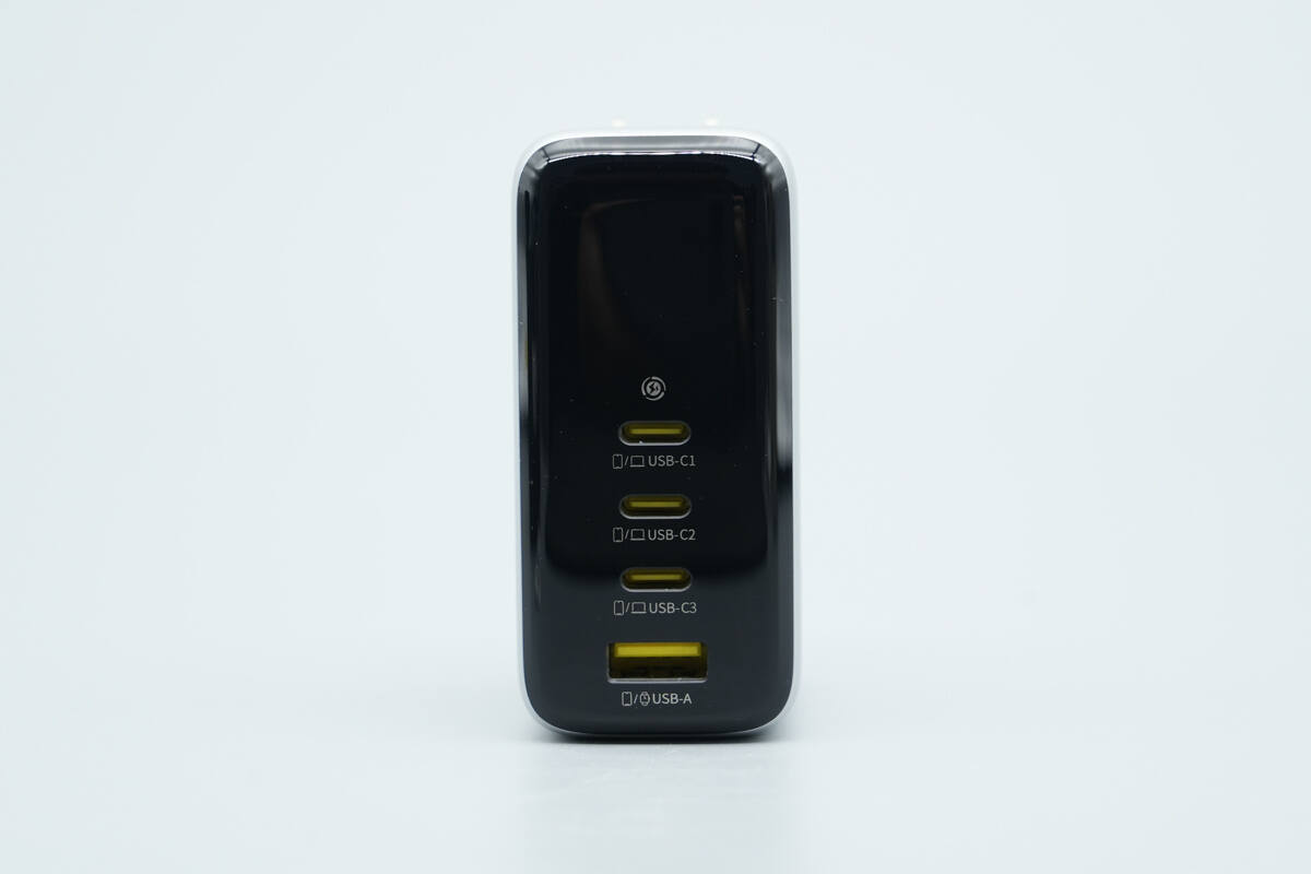
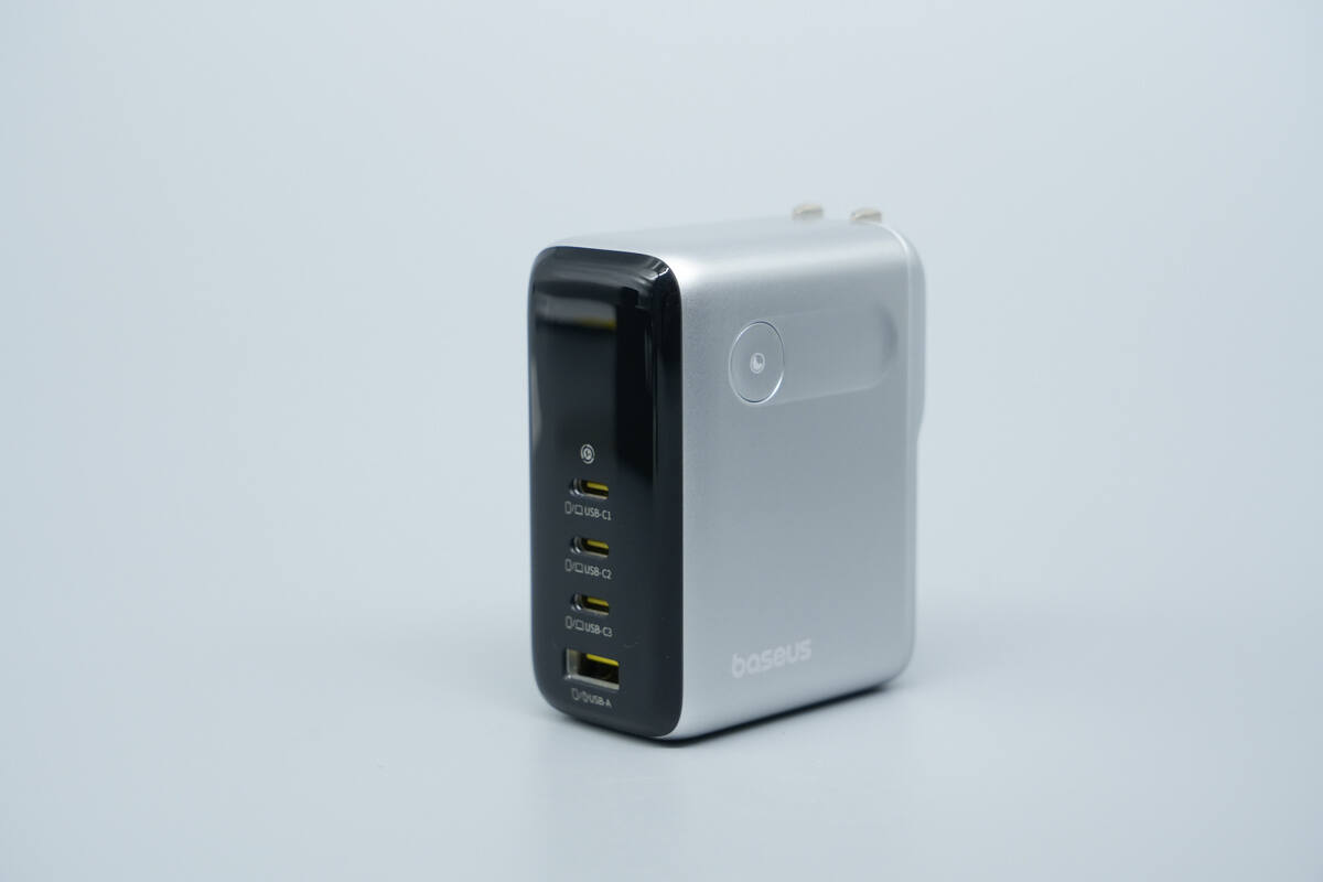
The output end is equipped with three USB-C ports and one USB-A port. The screen on top features UV-strengthened treatment, making it scratch-resistant, wear-resistant, and less prone to fingerprints.
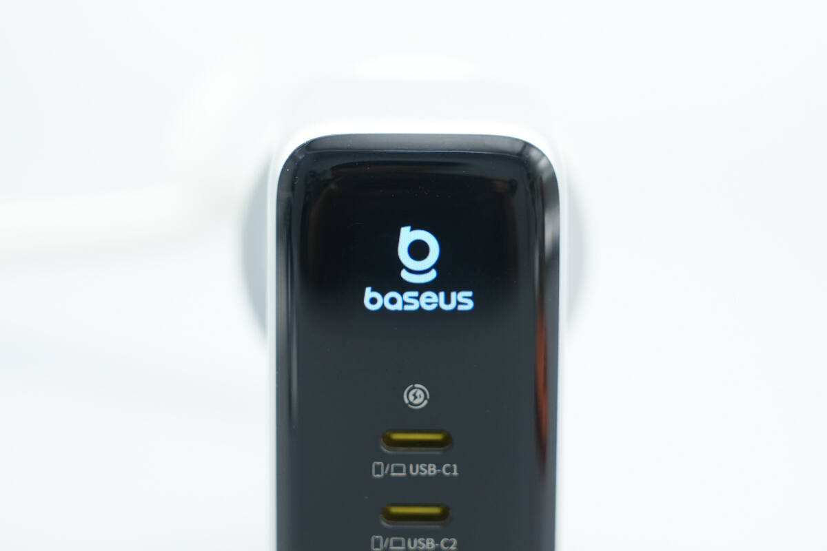
The screen lights up when powered on.

The multi-port power interface can be viewed at a glance, and double-pressing the button allows the interface to rotate 90°.
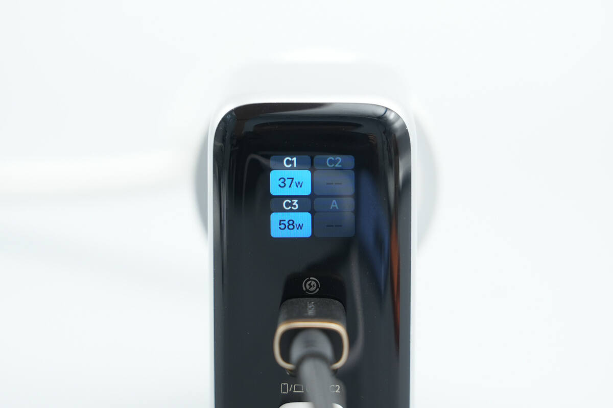
It can display the real-time output power of each individual port.

It can also display the output voltage and current for each individual port in detail.
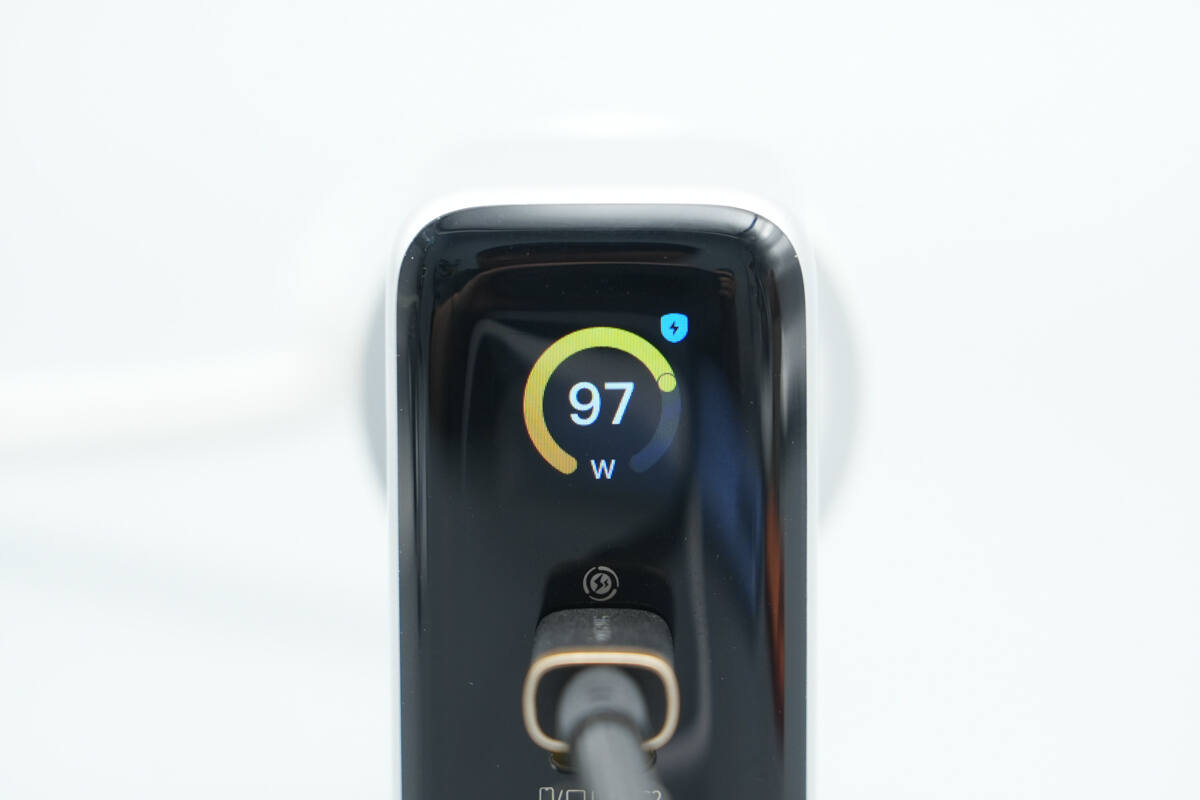
The total power interface can display the charger’s overall output power in real time.
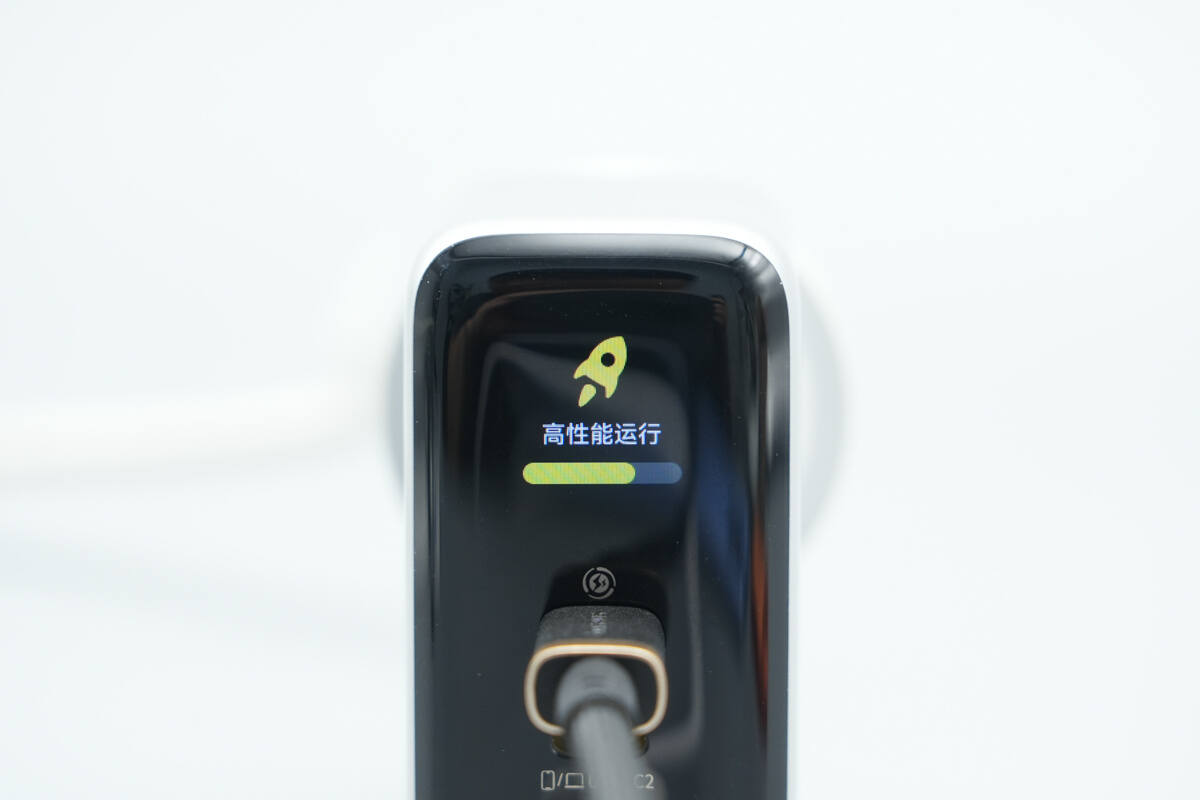
The operating mode interface provides a real-time overview of the charger’s working status.
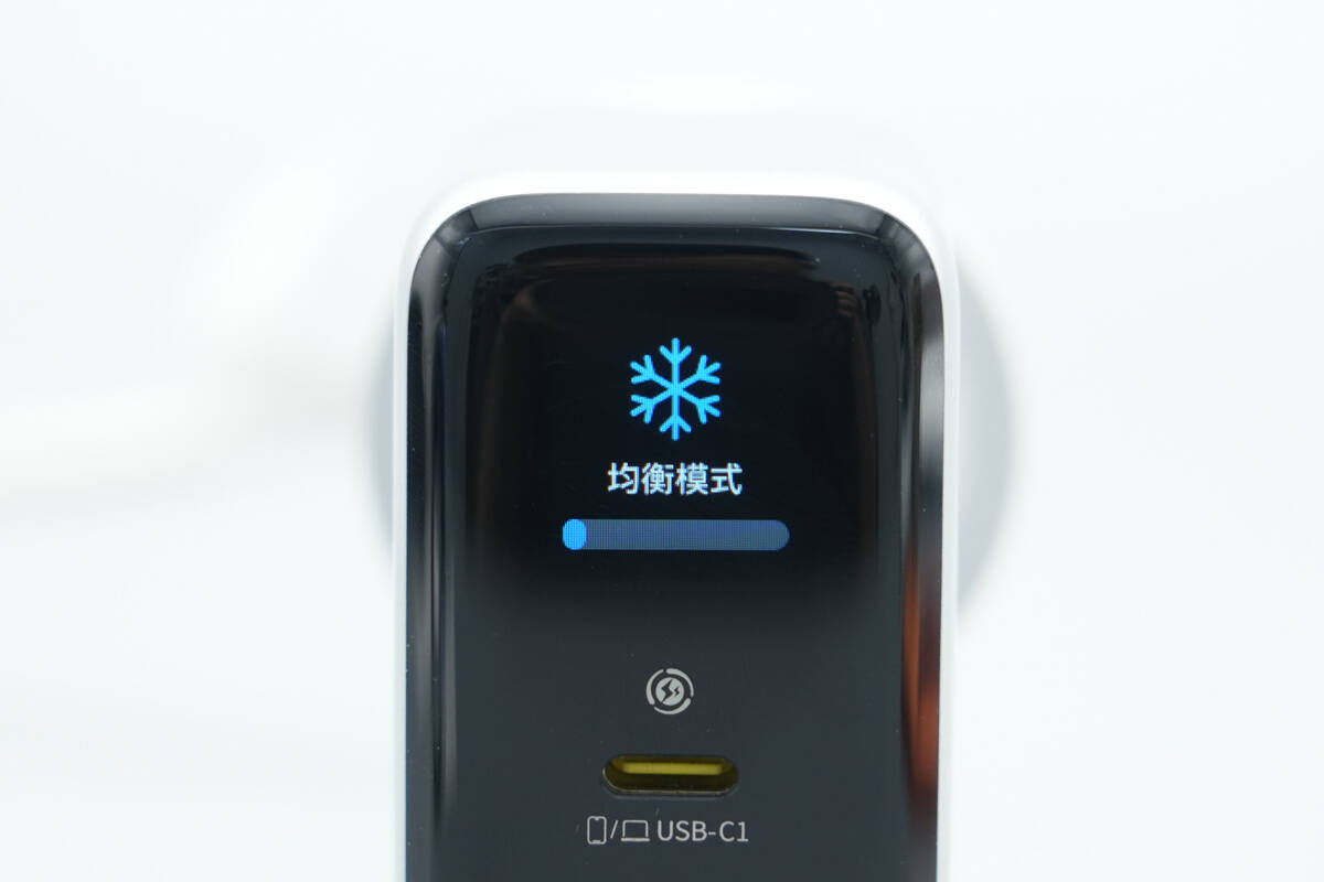
It can also visually indicate the temperature status using an energy bar format.
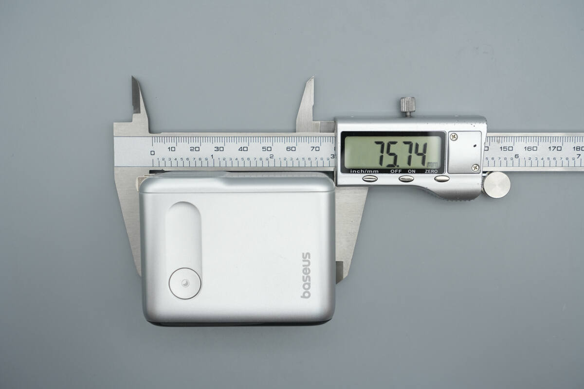
The length of the charger is about 75.74 mm (2.98 inches).
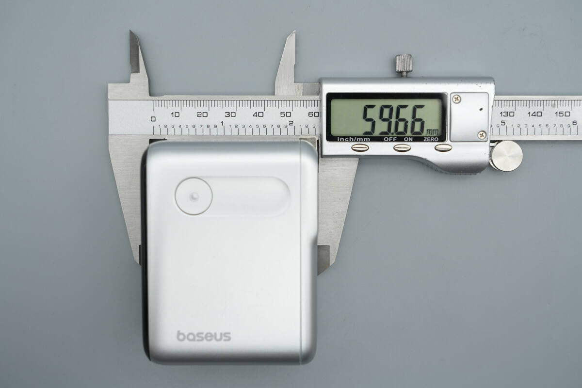
The width is about 59.66 mm (2.35 inches).
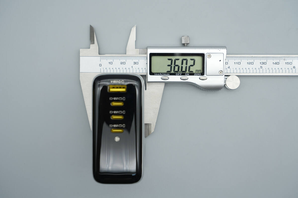
The thickness is about 36.02 mm (1.42 inches).
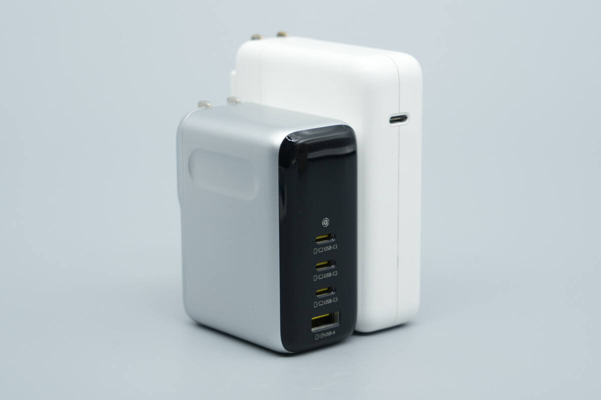
Compared with the Apple 140W charger, its size advantage is obvious.
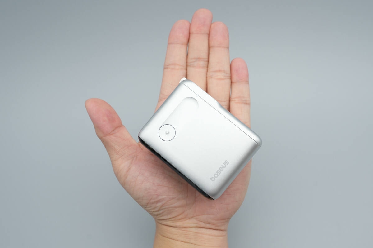
That's how big it is on the hand.
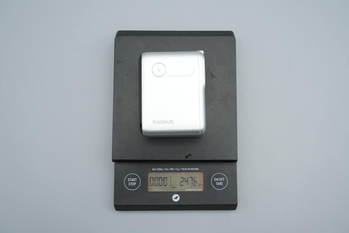
The weight is about 248 g (8.75 oz).
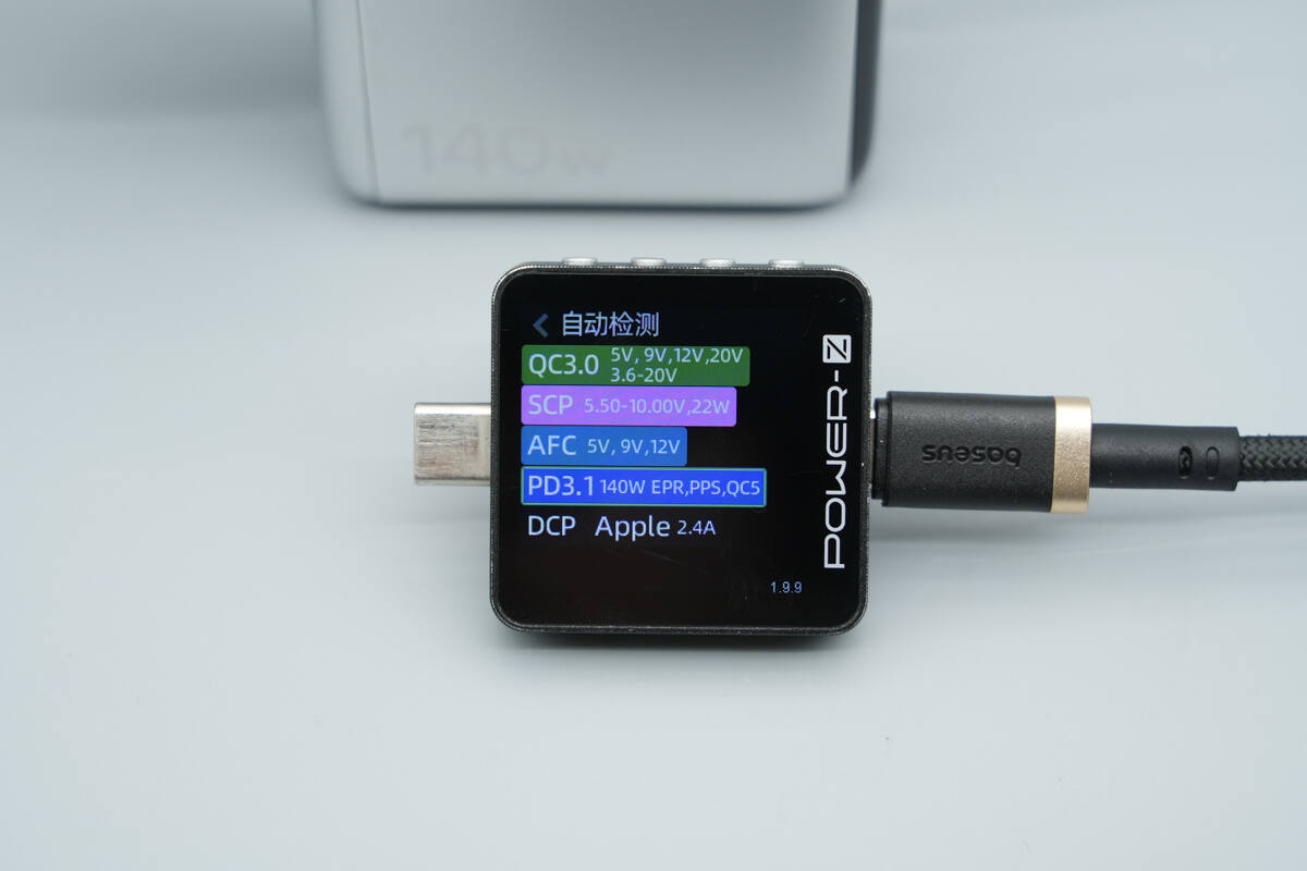
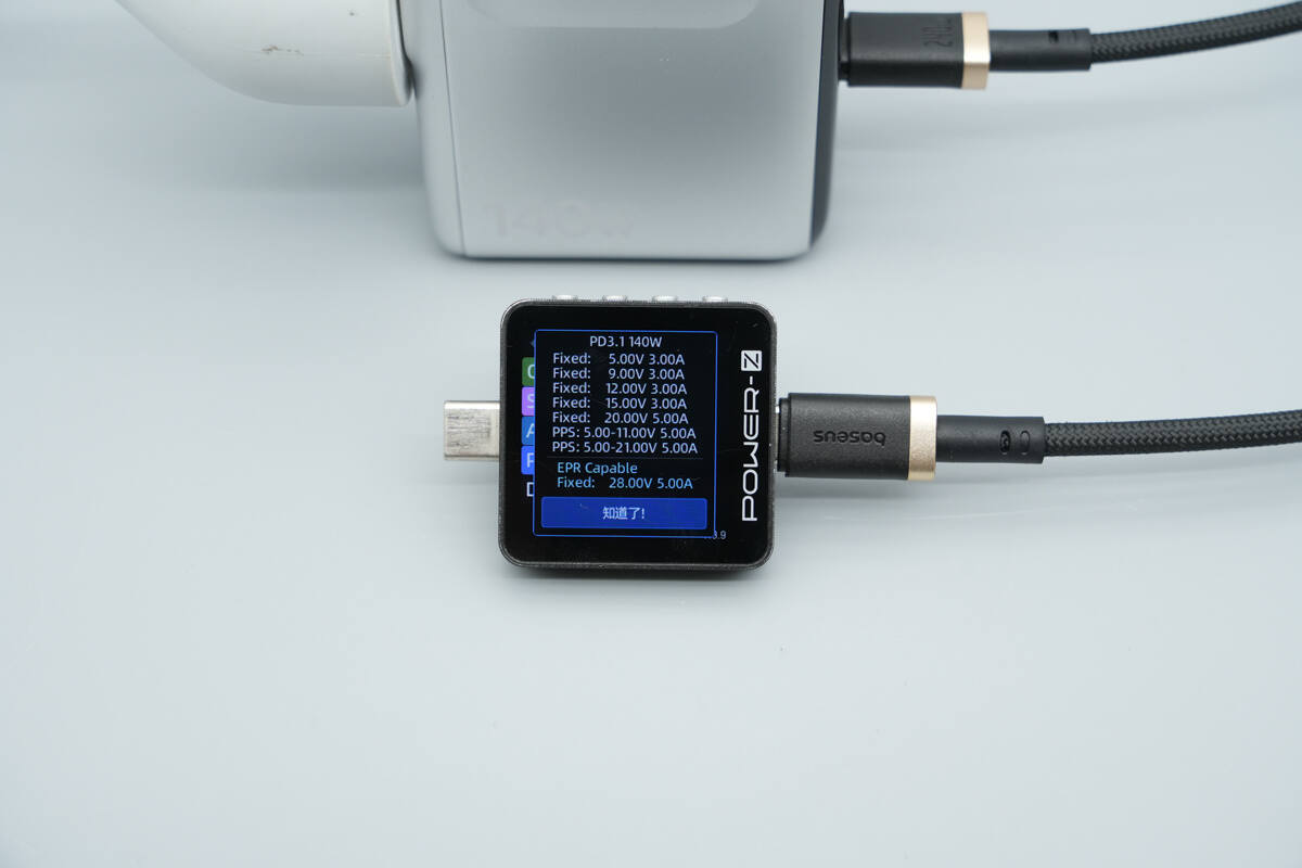
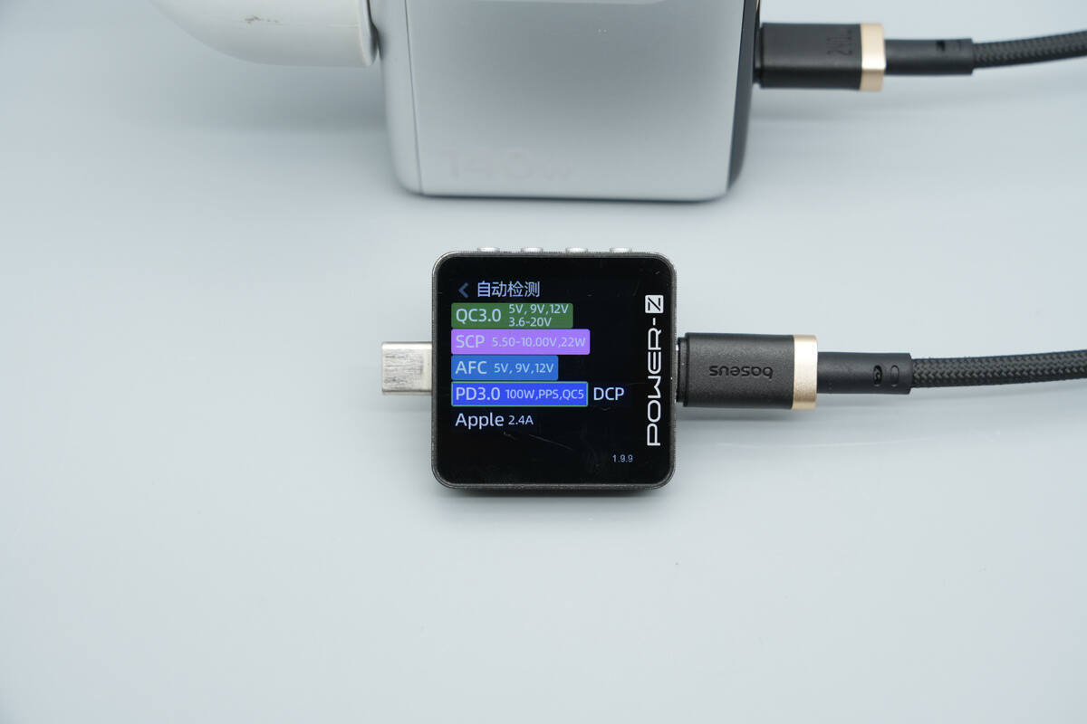
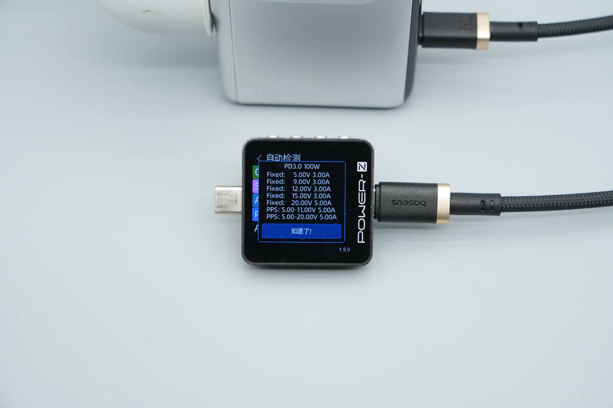
The USB-C1 supports QC3.0/5, SCP, AFC, PD3.1, PPS, DCP, and Apple 2.4A protocols.

It has six fixed PDOs of 5V3A, 9V3A, 12V3A, 15V3A, 20V5A, and 28V5A, along with two sets of PPS, which are 5-11V5A and 5-21V5A.
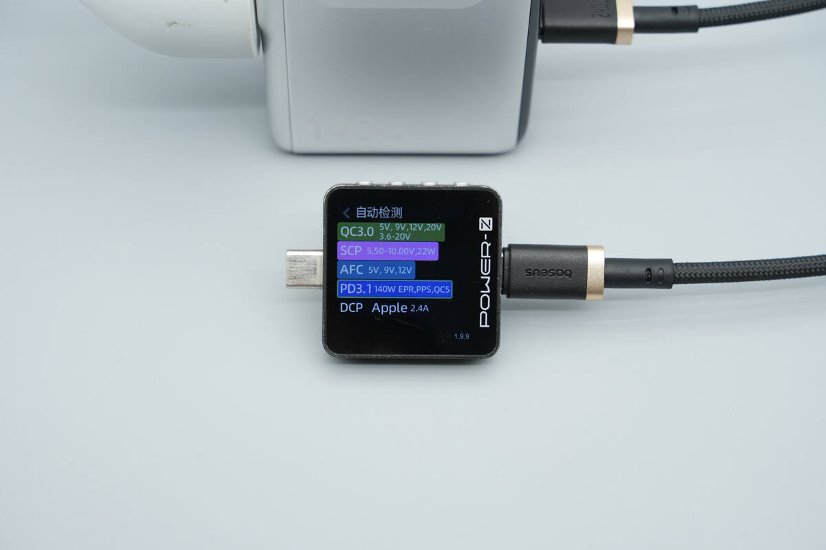
The USB-C2 port supports the same protocols as the USB-C1 port.
The PDO profiles are also identical.
The USB-C3 supports QC3.0/5, SCP, AFC, PD3.0, PPS, DCP, and Apple 2.4A protocols.
It has five fixed PDOs of 5V3A, 9V3A, 12V3A, 15V3A, and 20V5A, along with two sets of PPS, which are 5-11V5A and 5-20V5A.
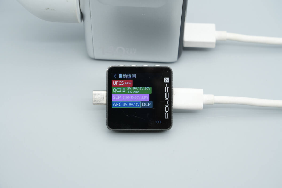
The USB-A supports UFCS, QC3.0, SCP, AFC, and DCP protocols.
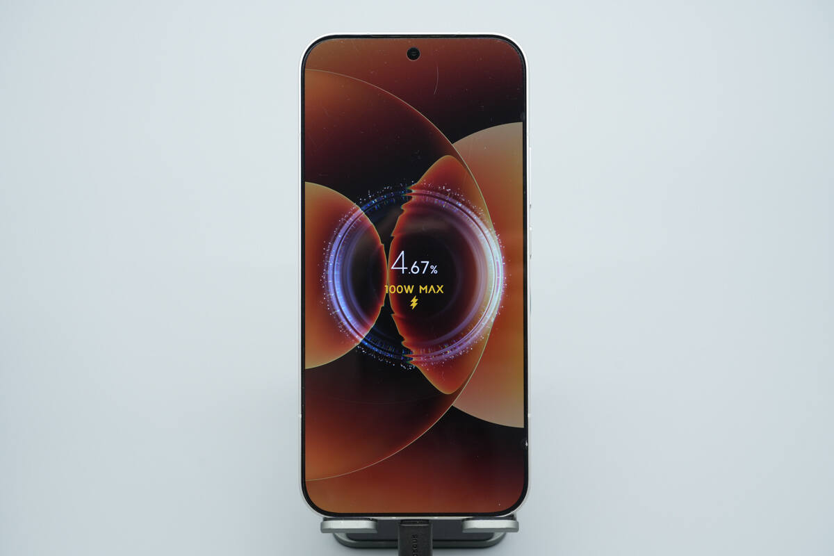
It also supports Xiaomi’s 120W Surge Fast Charging. When used to charge the Xiaomi 17 Pro Max, it successfully activated 100W Surge Fast Charging.
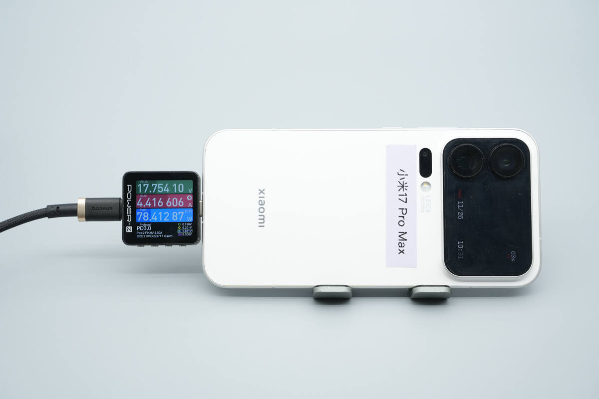
The charging power is approximately 78.41W.
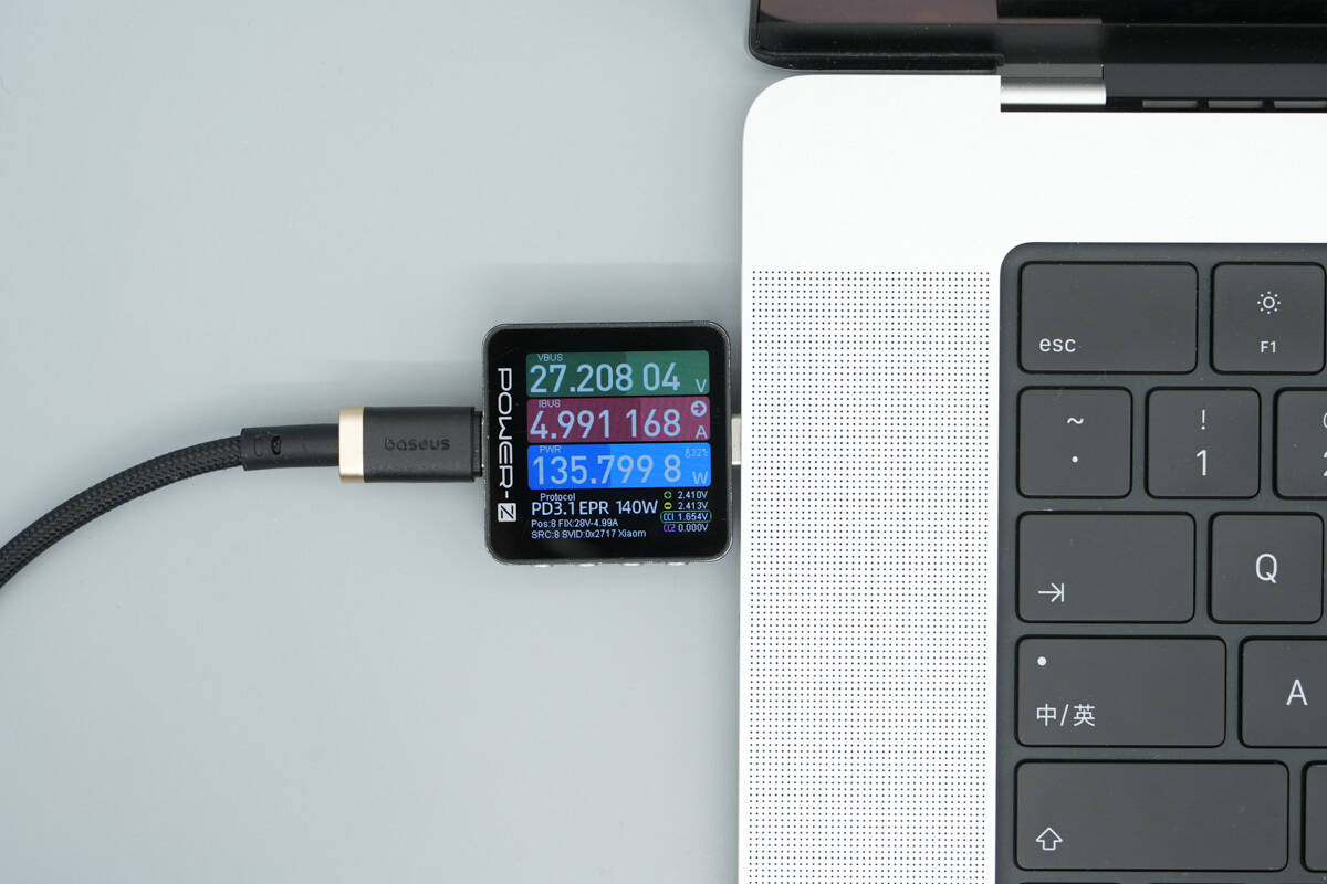
When used to charge a MacBook Pro, the power reaches approximately 135.8W, successfully activating 140W PD 3.1 fast charging.
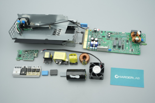
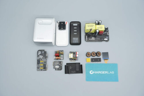
Teardown
Next, let's take it apart to see its internal components and structure.
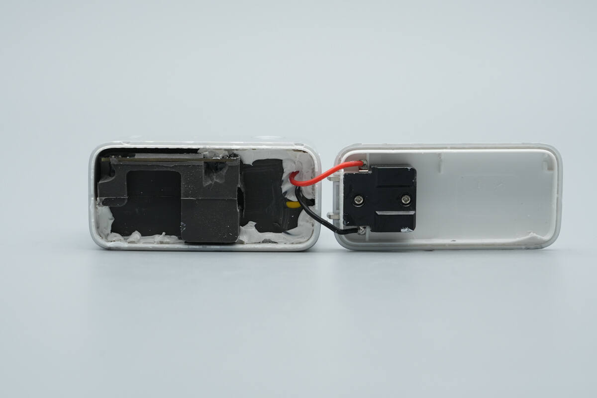
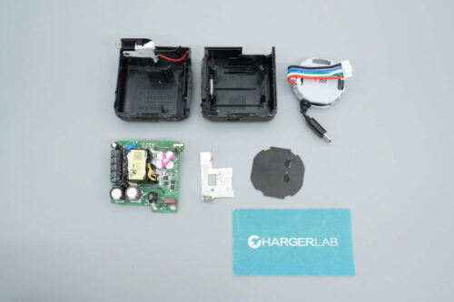
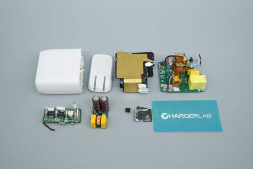
Remove the input connector housing. The prongs are secured with a plastic plate and screws, and connected to the PCBA module via wires.
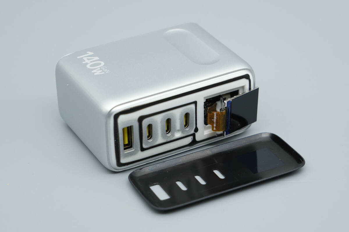
Remove the output panel. The screen is connected to the PCBA module via a ribbon cable.
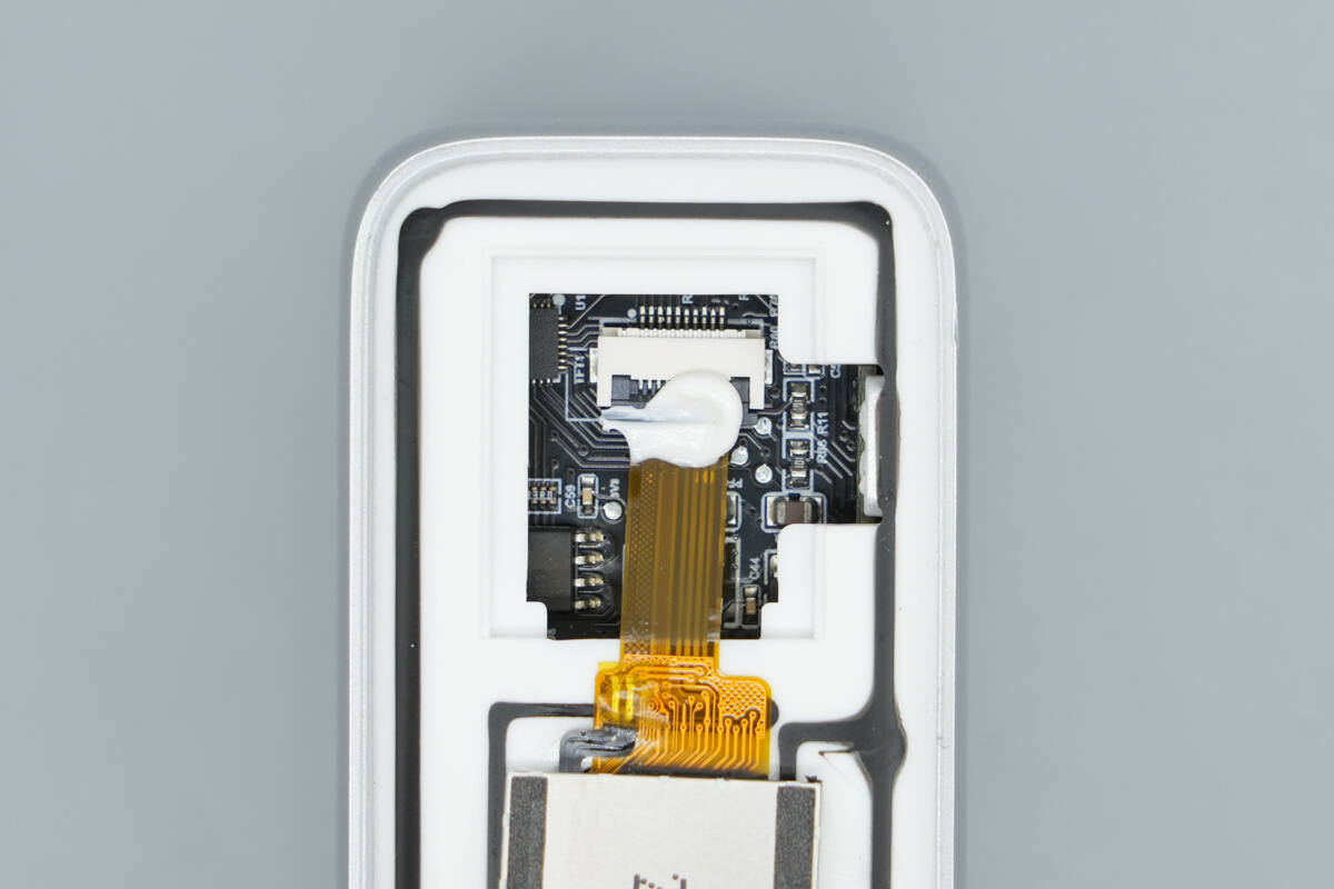
The connector is reinforced with adhesive sealing.

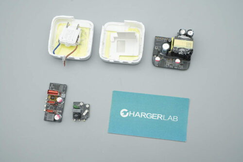
Remove the PCBA module.
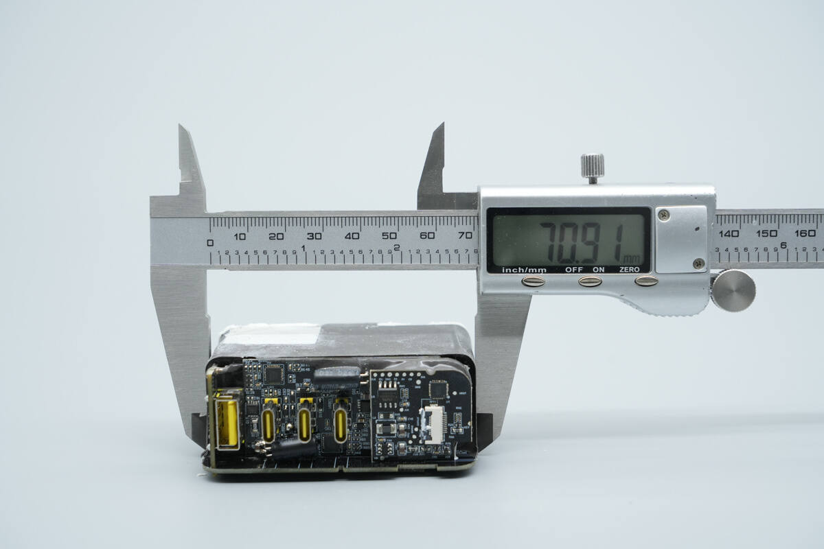
The length of the PCBA module is about 70.91 mm (2.79 inches).
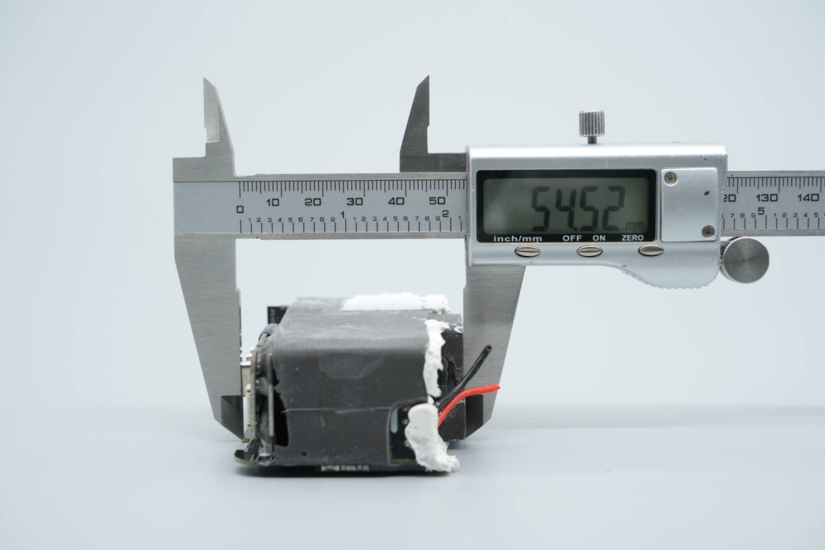
The width is about 54.52 mm (2.15 inches).
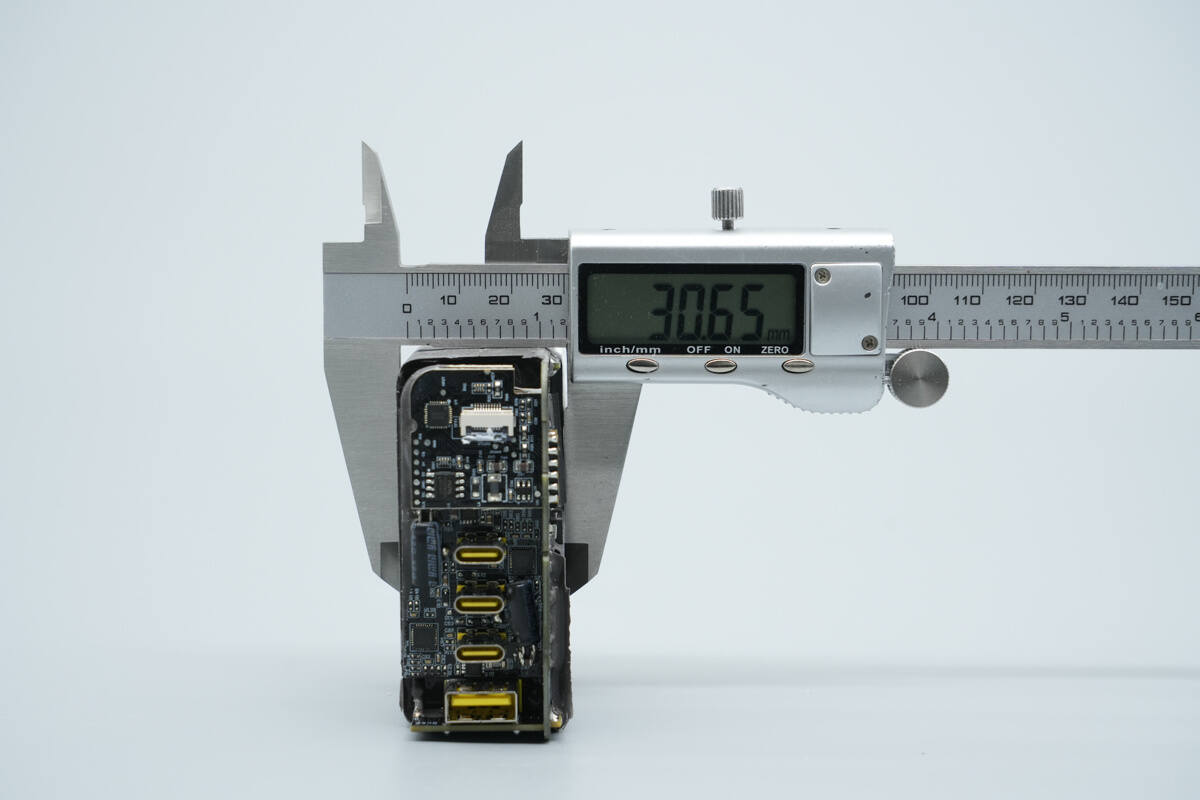
The thickness is about 30.65 mm (1.21 inches).
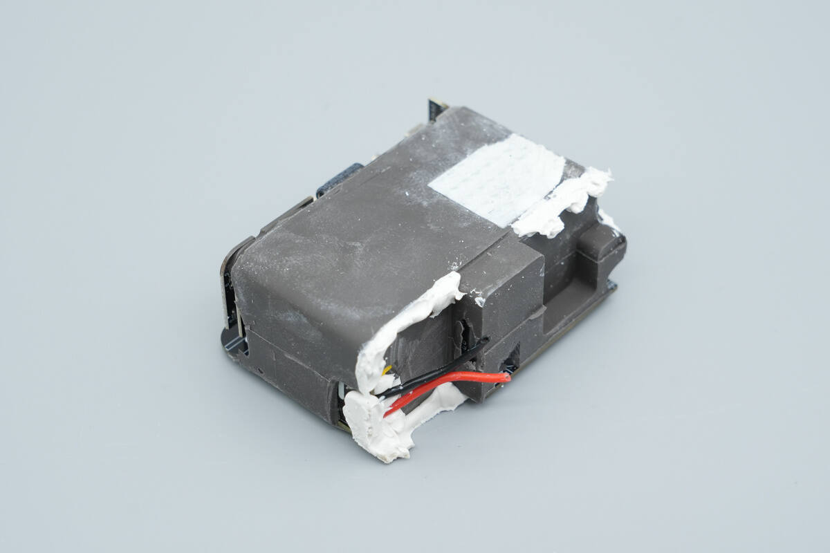
The PCBA module is encapsulated with adhesive to enhance weather resistance and heat dissipation performance.
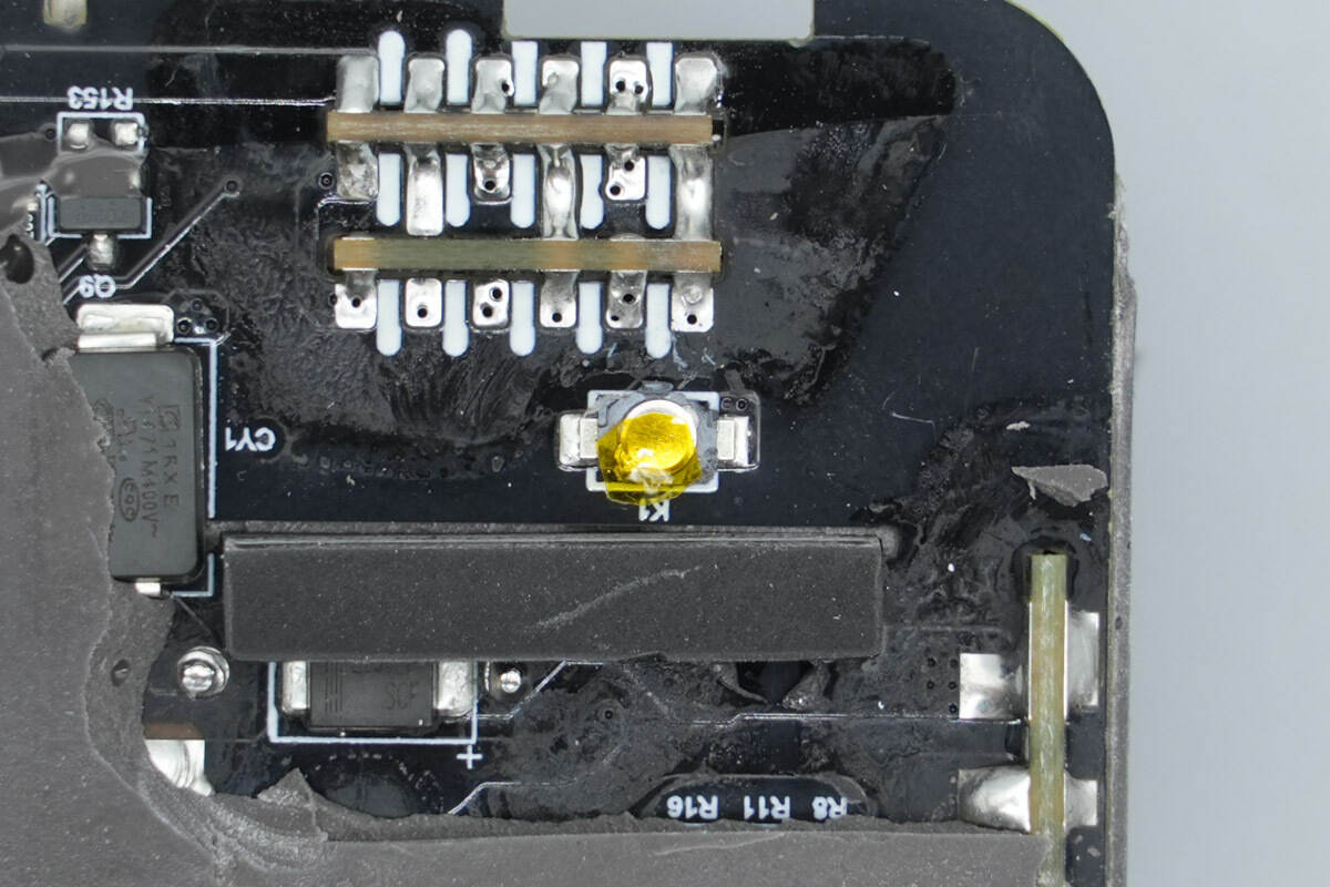
The function button area is covered with adhesive tape.

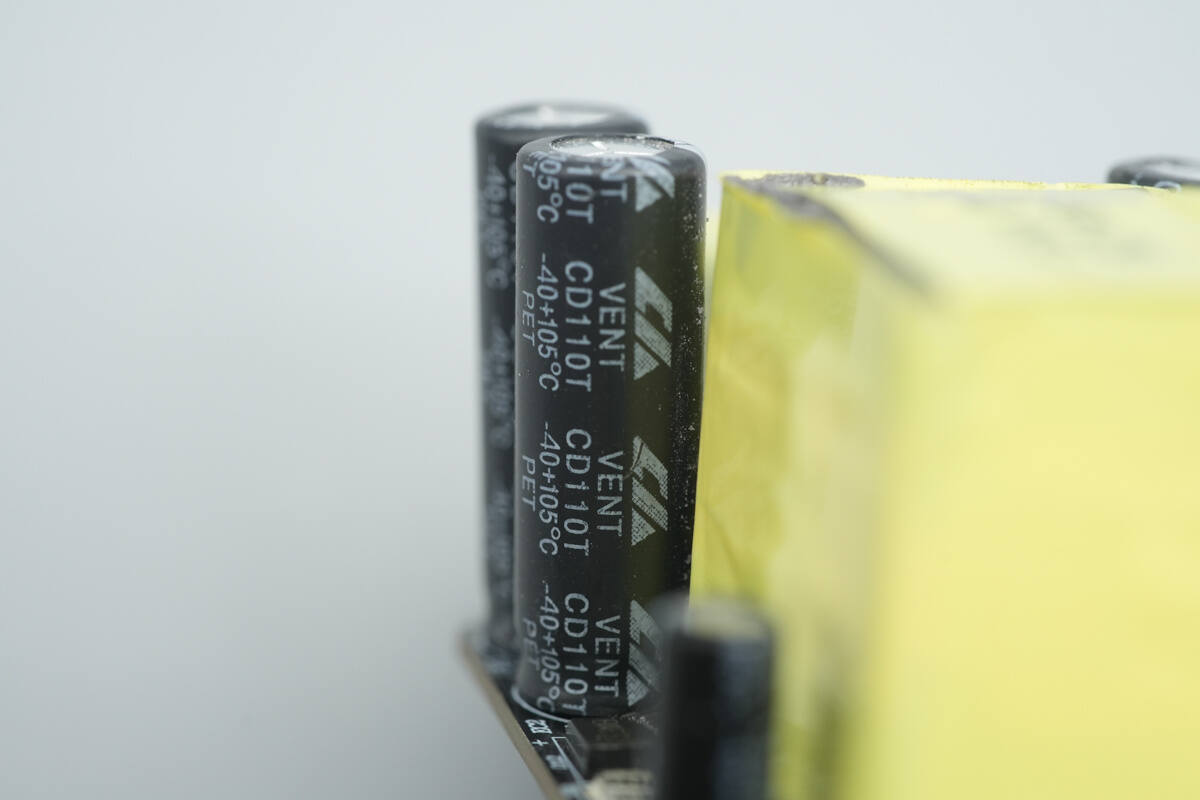
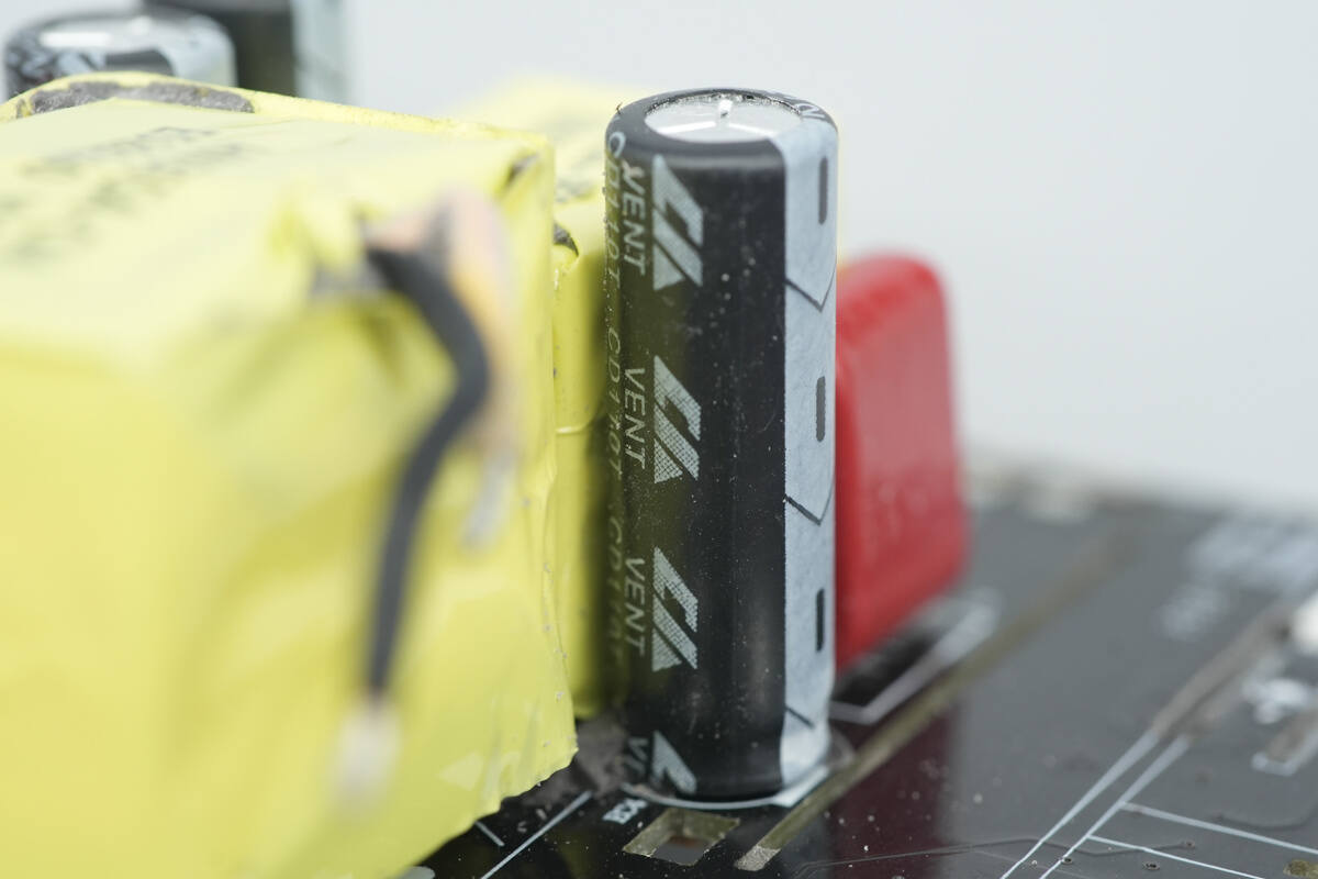
The PCBA module is cleaned. Small PCBs are installed on both sides of the module as well as at the output end.
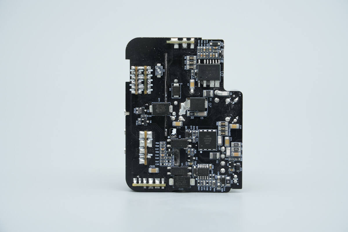
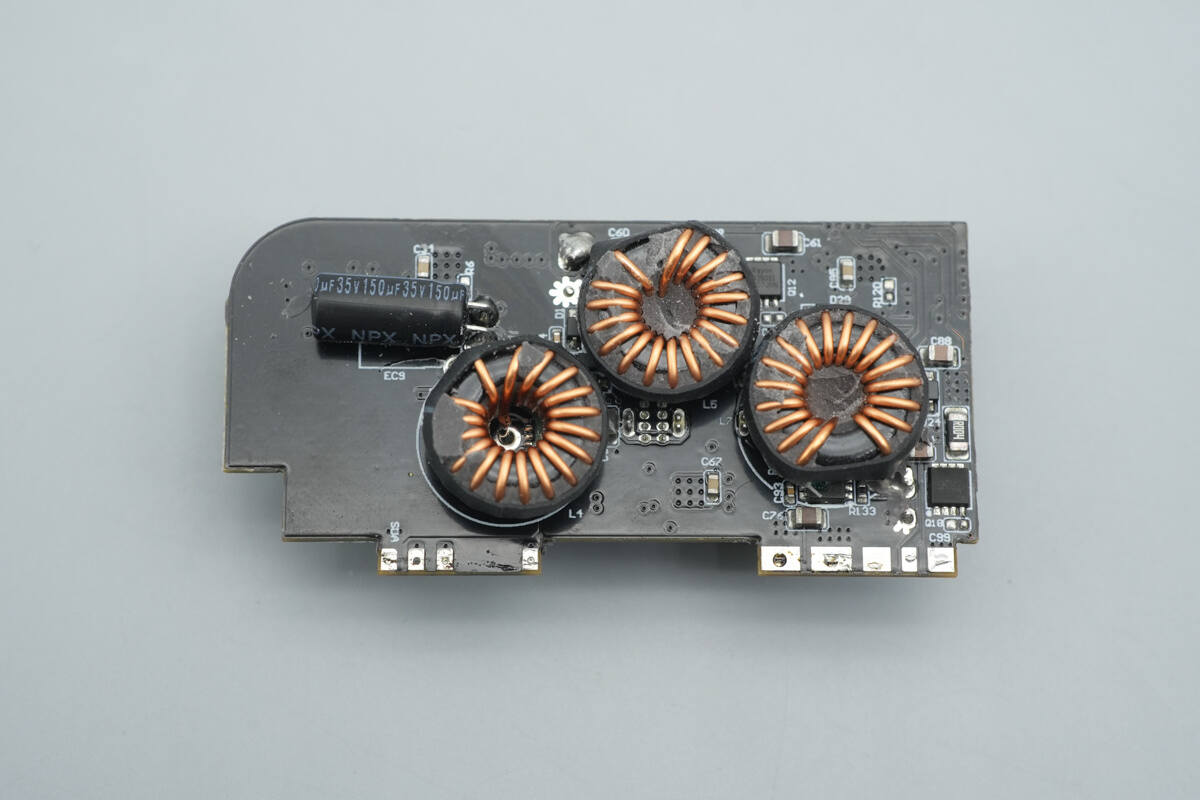
The backside of the PCBA module features components such as the PFC controller, PFC rectifier, master control chip, primary MOSFET, optocouplers, and SMD Y capacitors.
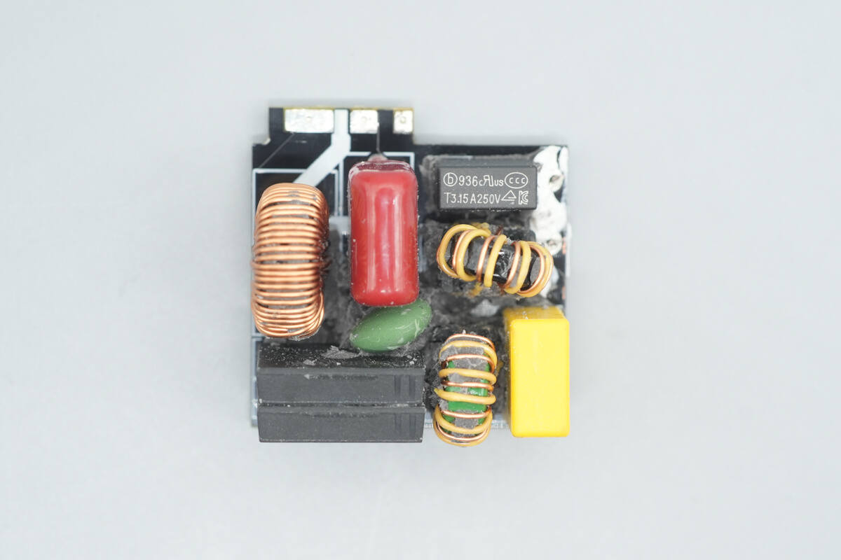
Remove the output small PCB. Its front side contains a time-delay fuse, common mode chokes, a safety X2 capacitor, an NTC thermistor, bridge rectifiers, a film capacitor, and a filter inductor.
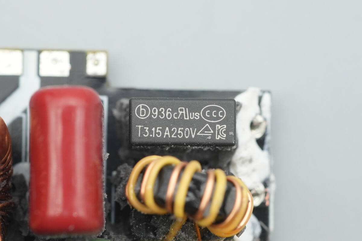
The time-delay fuse is from Betterfuse, part number 936, rated at 3.15A 250V.
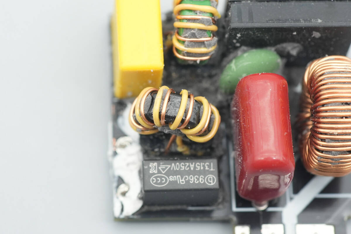
The common mode choke is used to filter out EMI interference.
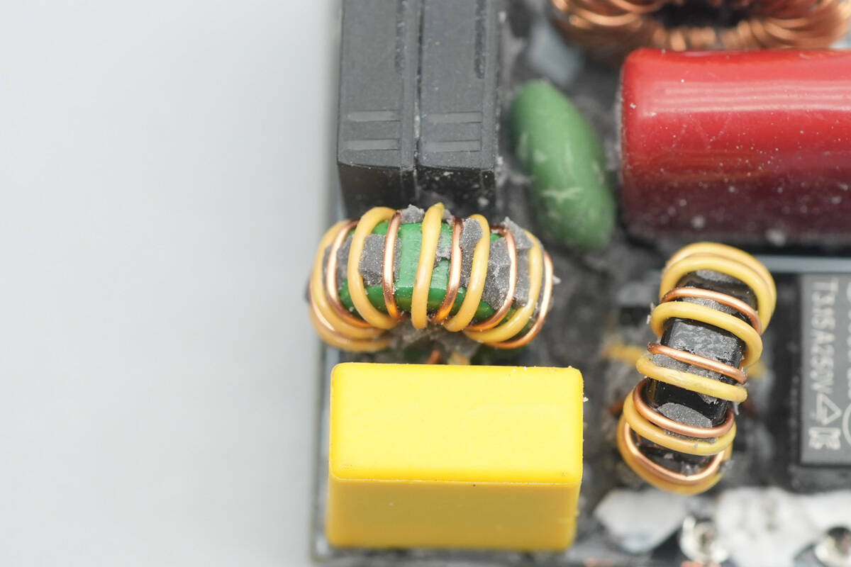
Close-up of the other common mode choke.
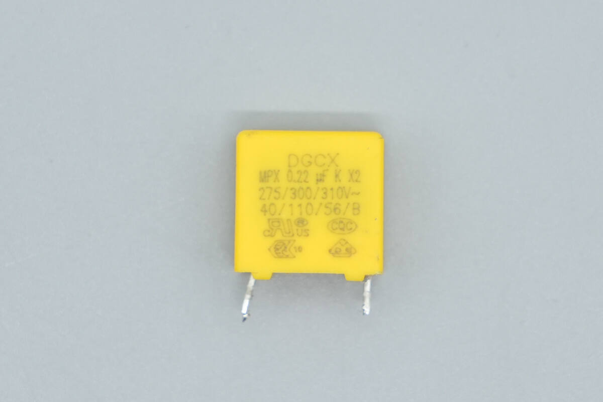
The safety X2 capacitor is from DGCX, with a capacitance of 0.22μF.
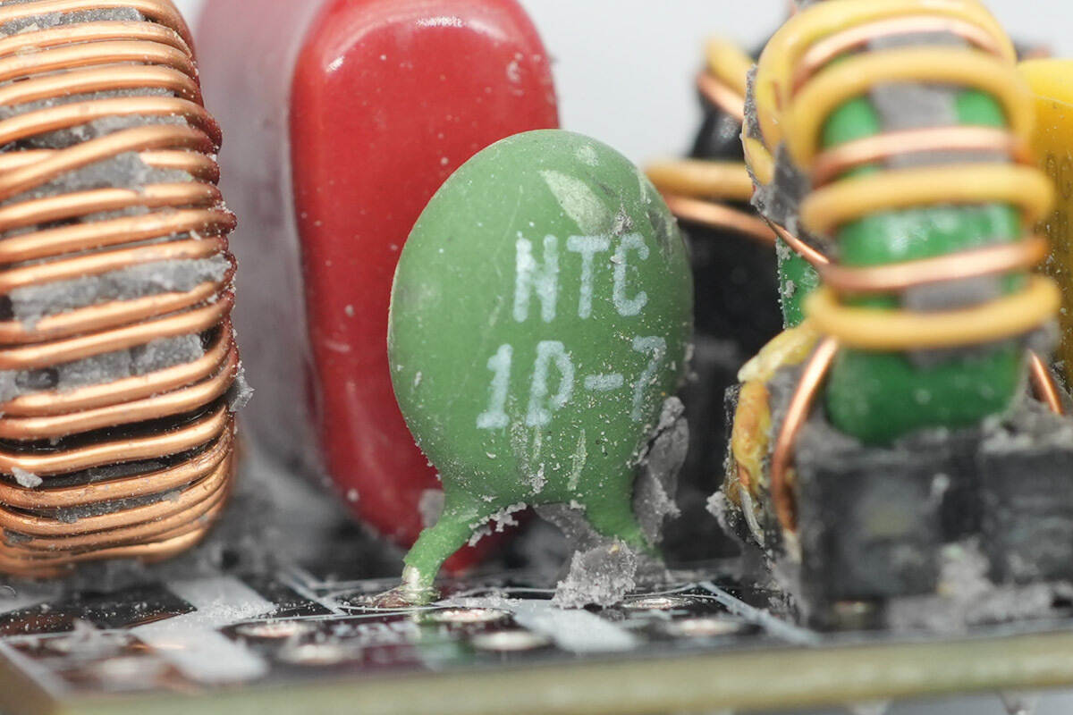
The NTC thermistor is used to suppress inrush current during power-on.
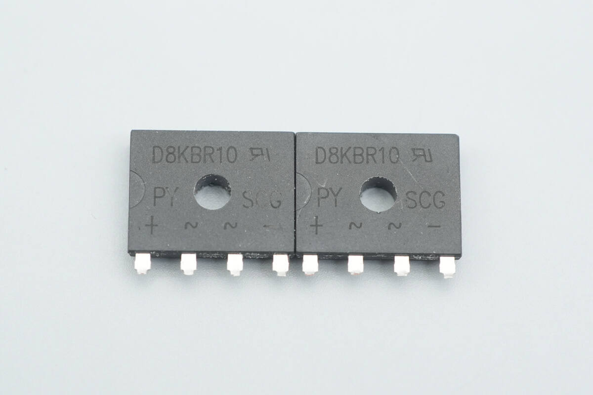
The two bridge rectifiers are from PY, model D8KBR10A, rated at 8A 1000V, and use the D3K package.

The film capacitor is from DGCX, with a specification of 1μF 450V.
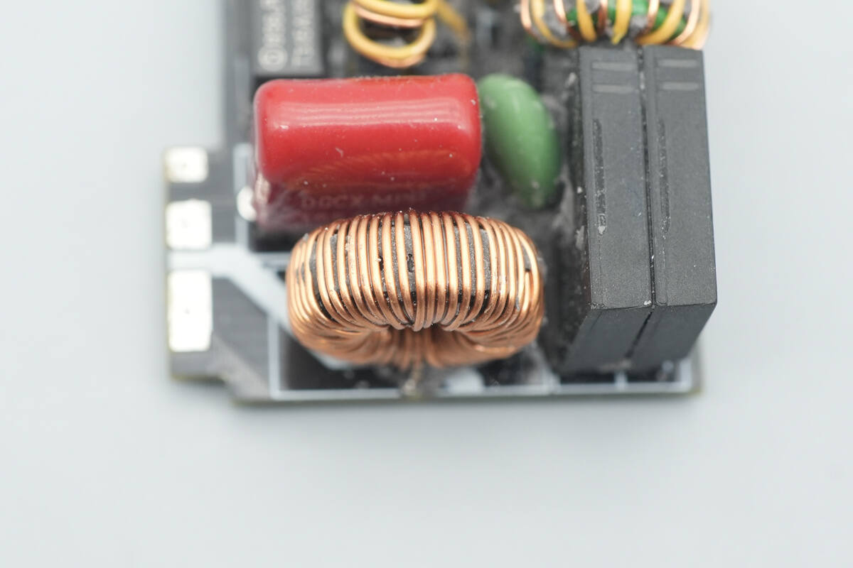
Close up of the filter inductor.
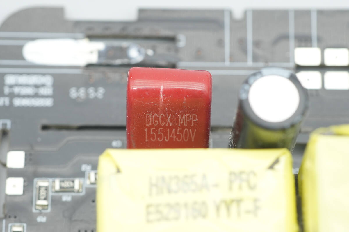
The other film capacitor is also from DGCX, with a specification of 1.5μF 450V.
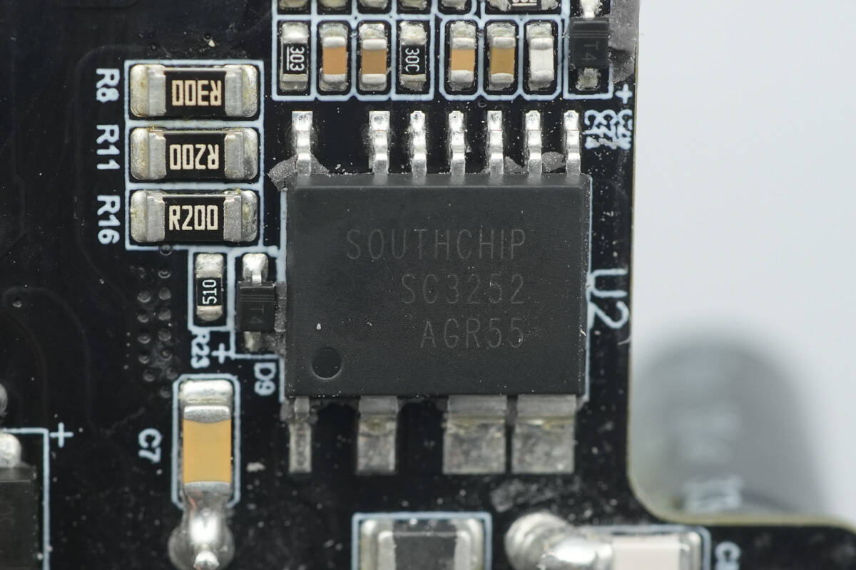
The PFC controller is from SouthChip, model SC3252. This is an efficient CrMBoost PFC controller integrated with 650V GaN, designed for boost converters. The SC3252 achieves high performance through a multi-mode control strategy. It operates in critical conduction mode (CrM) under heavy or full load conditions. As the load decreases, it switches to discontinuous conduction mode (DCM), using valley switching and reduced frequency to enhance efficiency. In no-load conditions, the chip enters burst mode to reduce power consumption and minimize audio noise.
By combining the SC3252 with a flyback controller and secondary synchronous rectification controller, high efficiency can be achieved across the entire load range, and the system can easily meet the stringent standby power requirements to comply with efficiency regulations. Thanks to the SC3252, the PFC stage can achieve a near unity power factor and sinusoidal input current with minimal external components.
The SC3252 provides comprehensive protection features to prevent damage to the circuit under abnormal conditions. The chip is housed in an ESOP-10W package, simplifying user design and reducing system costs.
Close up of the PFC boost inductor.
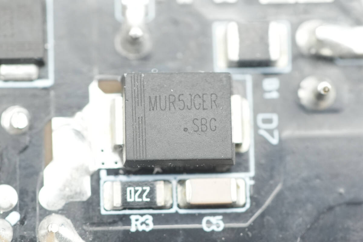
The PFC rectifier is from PY, model MUR5JGER. It is an ultra-fast recovery diode with a rated current of 5A and a voltage rating of 600V, housed in an SMC package.
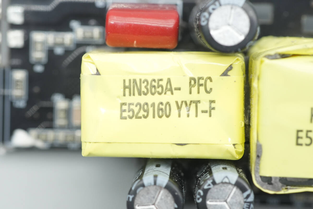
The two high-voltage filtering electrolytic capacitors are from ChuangHui.
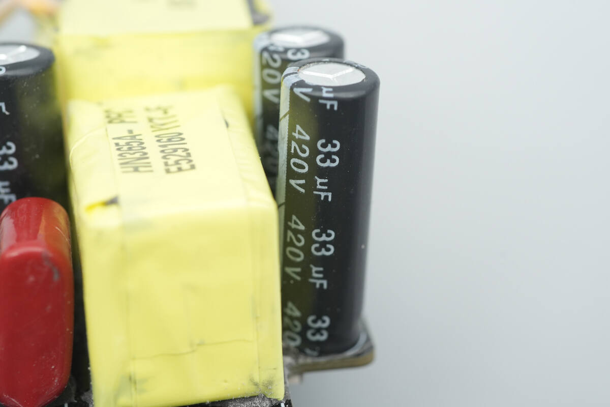
Both are rated at 420V, 33μF.
The third high-voltage filtering electrolytic capacitor is also from ChuangHui.
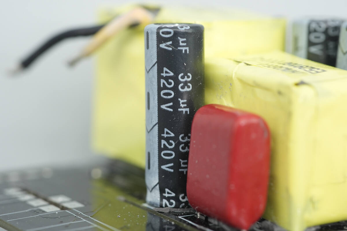
Its specification is also 420V, 33μF.
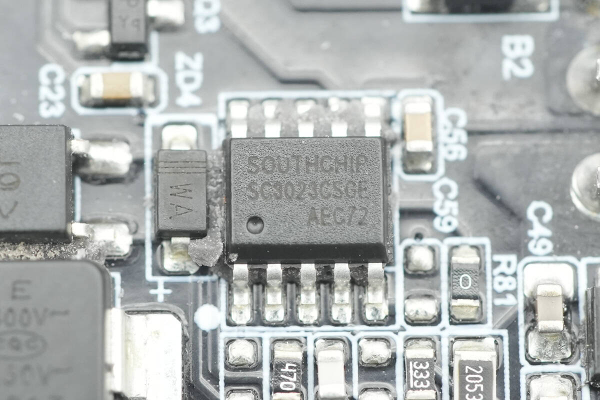
The master control chip is from SouthChip, model SC3023. It is a high-frequency quasi-resonant flyback controller with built-in GaN drive, capable of directly driving GaN FETs. The SC3023 features X-capacitor discharge and high-voltage startup, and includes adaptive switching frequency foldback to achieve higher efficiency across the entire load range. In QR and DCM modes, valley switching is used to improve efficiency. Under no-load conditions, it operates in a low-power mode to reduce system standby consumption. The chip also provides comprehensive protection features, supporting both internal and external over-temperature protection.
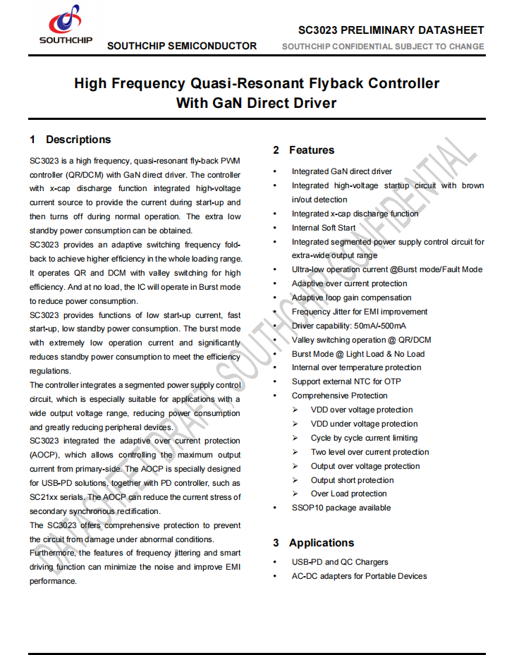
Here is the information about SouthChip SC3023.
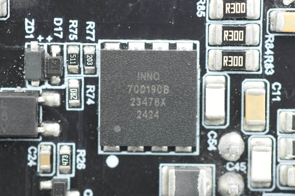
The primary MOSFET is from Innoscience, model INN700DA190B. It is a 700V enhancement-mode GaN transistor, upgraded from the previous 650V rating, with a transient voltage tolerance of 800V. The device has an on-resistance of 190 mΩ, supporting higher power applications.
It supports ultra-high switching frequencies, has no reverse-recovery charge, and features very low gate and output charge. It meets JEDEC standards for industrial applications and includes built-in ESD protection. The device is RoHS-compliant, lead-free, and conforms to EU REACH regulations, making it suitable for high-efficiency, high-density applications such as AC-DC and DC-DC conversion. It is housed in a DFN 5×6 package.
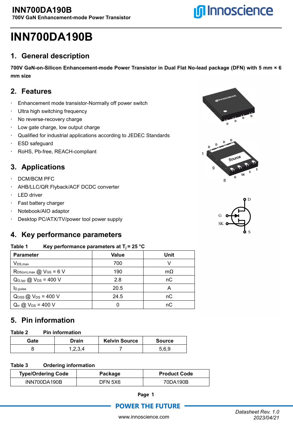
Here is the information about Innoscience INN700DA190B.
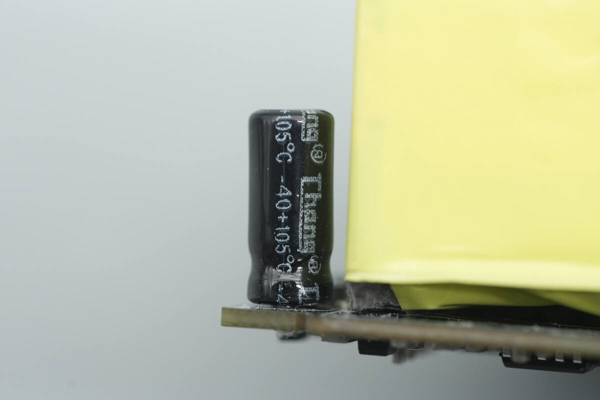
The capacitor supplying power to the master control chip is from Chang.
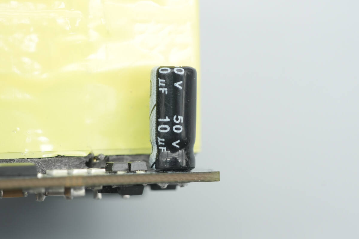
Its specification is 50V, 10 μF.
Close-up of the transformer.
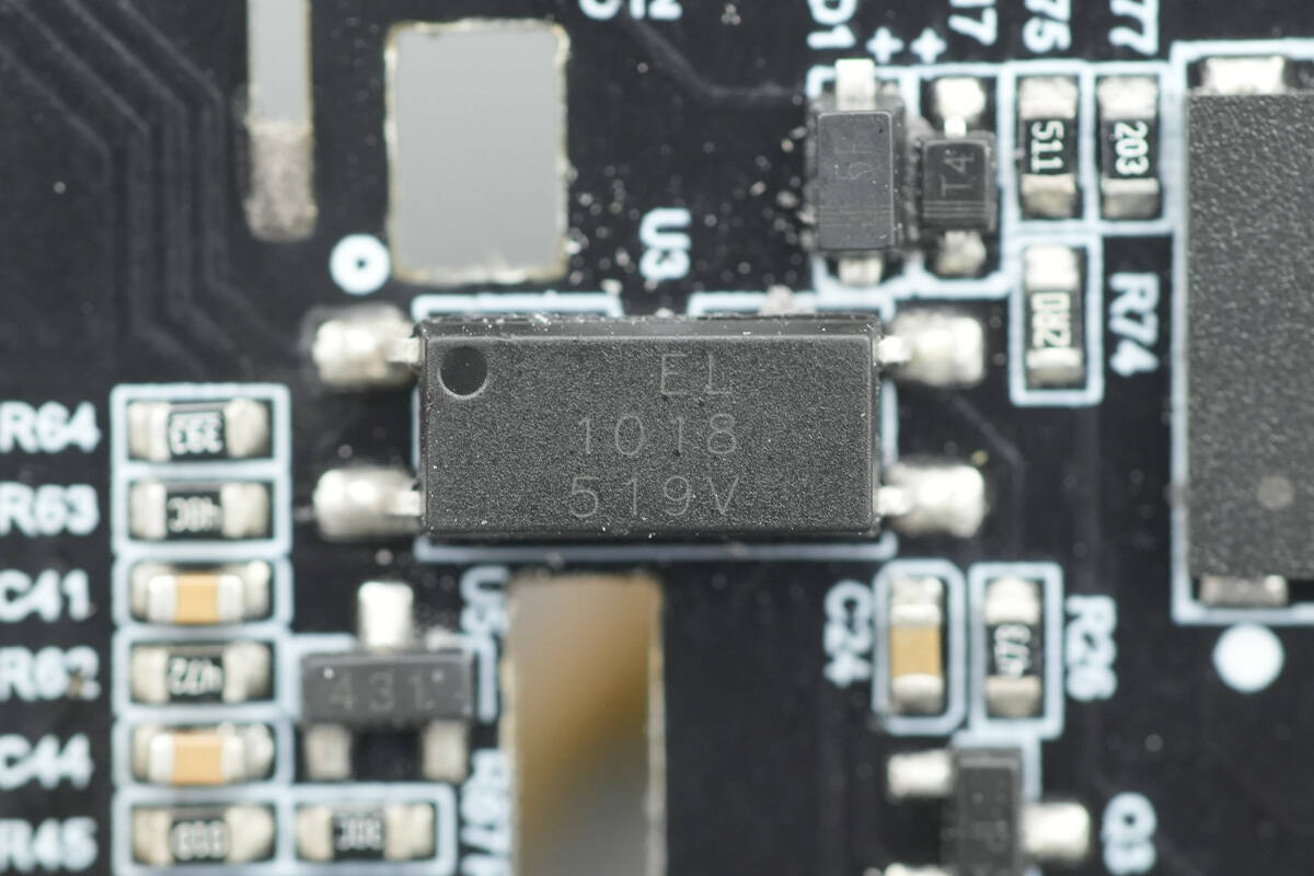
The Everlight EL1018 optocoupler is used for output voltage feedback.
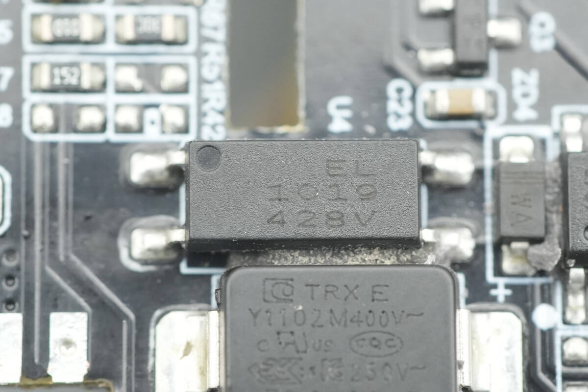
Close-up of the other Everlight EL1019 optocoupler.
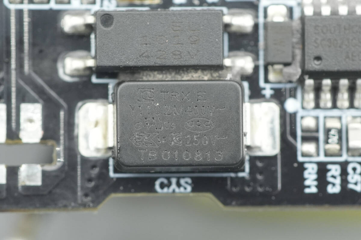
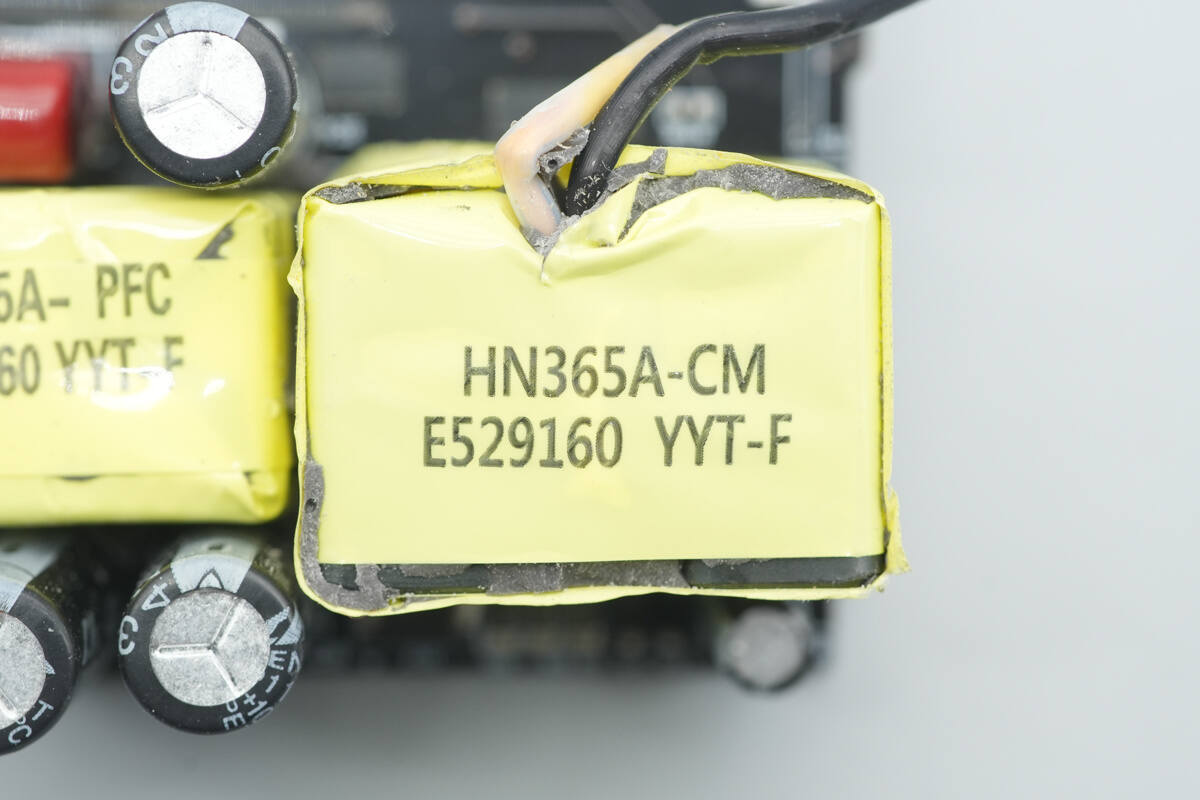
The SMD Y capacitor is from TRX, part number TMY1102M. Its compact size and light weight make it well-suited for high-density power products such as GaN fast chargers.
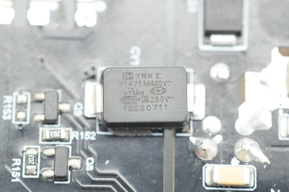
The other TRX SMD Y capacitor has the part number TMY1471M.
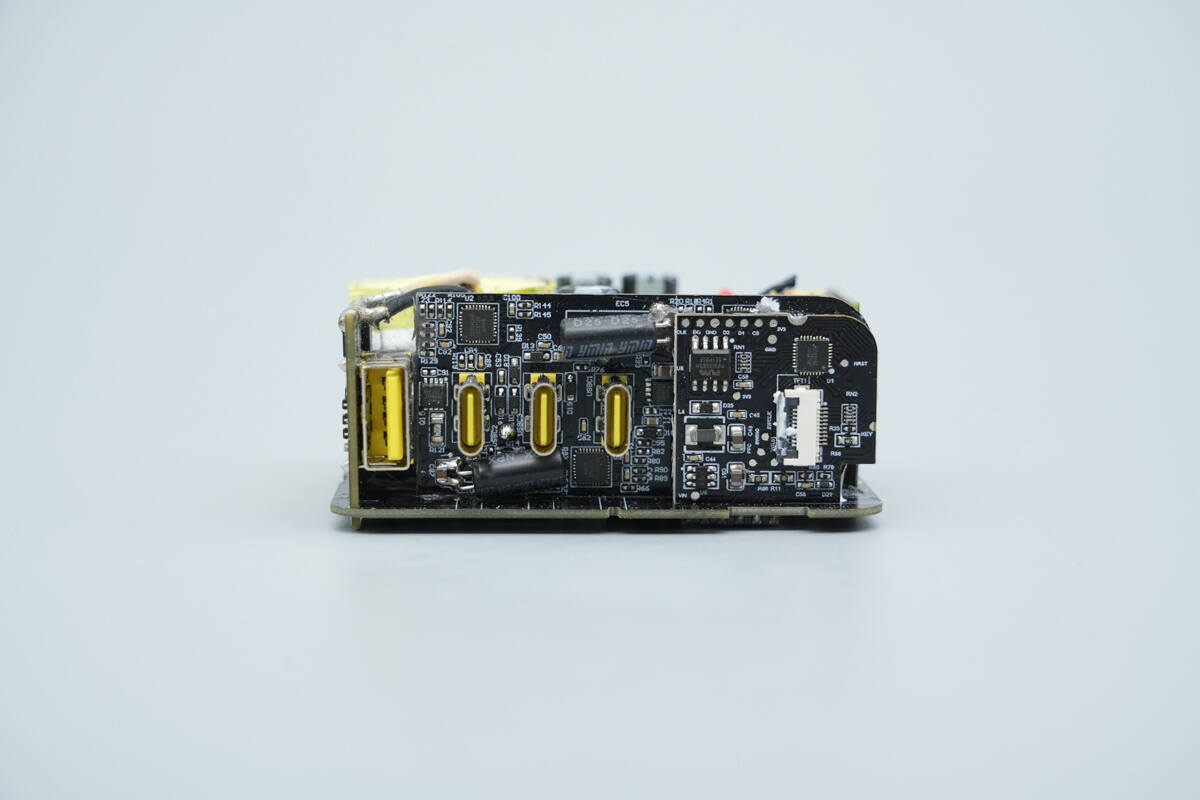
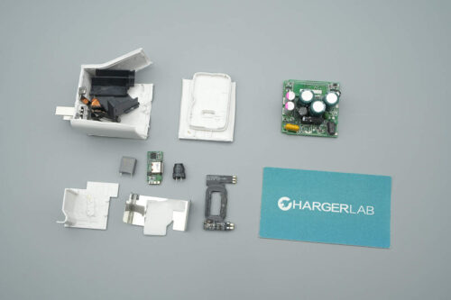
The USB-C port, USB-A ports, and the display control are all implemented on separate small PCBs.
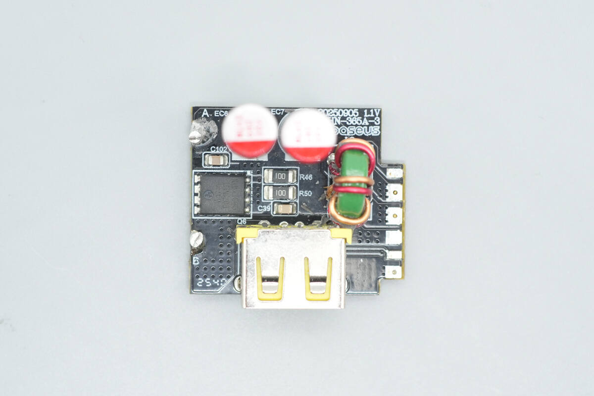
Remove the PCB housing the USB-A socket. On the front side, it features a synchronous rectifier, solid capacitors, and a filter inductor.
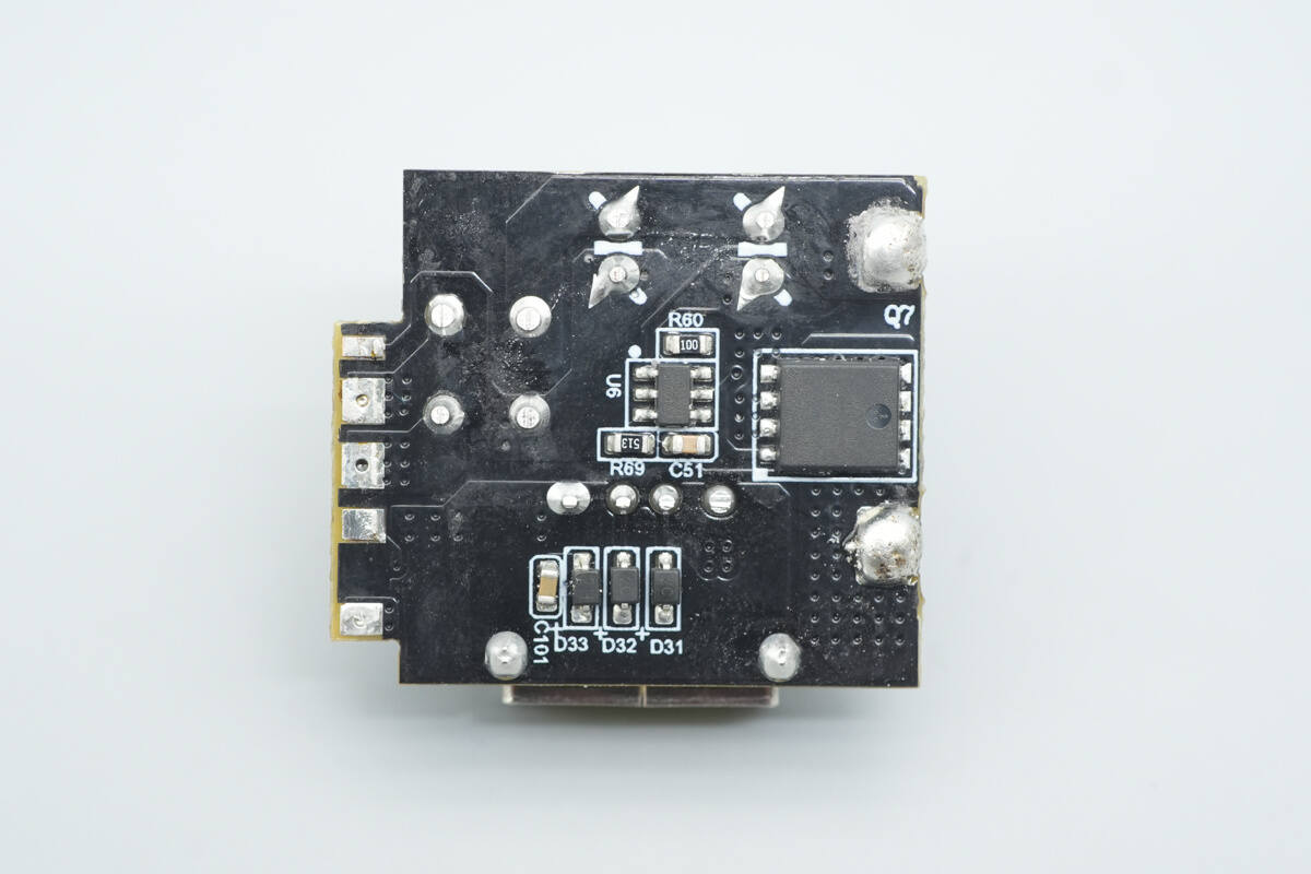
On the back side, it features the synchronous rectifier controller along with the synchronous rectifier.
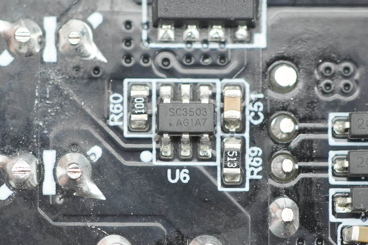
The synchronous rectifier controller is from SouthChip, model SC3503. It is an adaptive turn-on detection and fast turn-off synchronous rectifier controller that requires no auxiliary winding for power. The output voltage can go as low as 0 V. Its patented adaptive turn-on detection circuit prevents false activation of the synchronous rectifier and is compatible with various MOSFETs. The device features ultra-low quiescent current, supports multiple operating modes, and can control both high-side and low-side synchronous rectification, all with minimal external components.
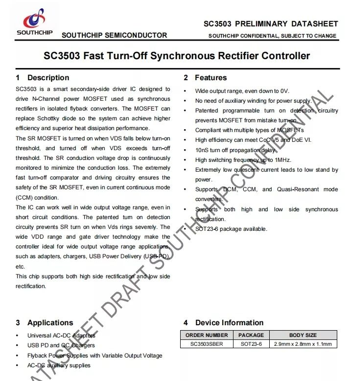
Here is the information about SouthChip SC3503.
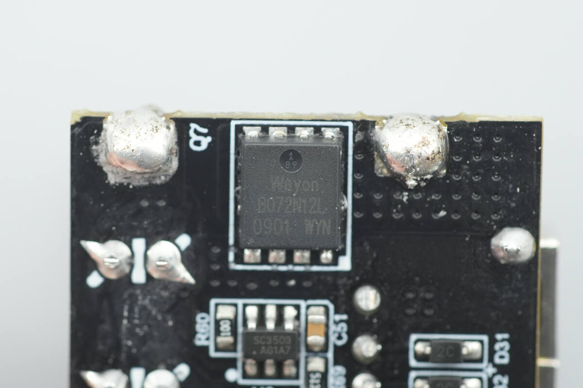
The synchronous rectifier is from WAYON, model WMB072N12LG2. It is an NMOS with a voltage rating of 120 V and an on-resistance of 7 mΩ, housed in a PDFN 5×6-8L package.
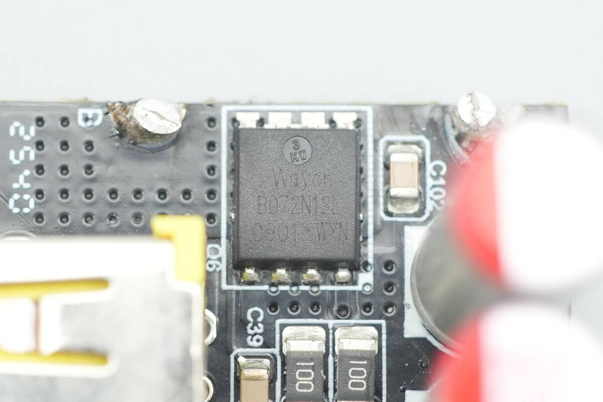
The other synchronous rectifier also uses the WAYON WMB072N12LG2.
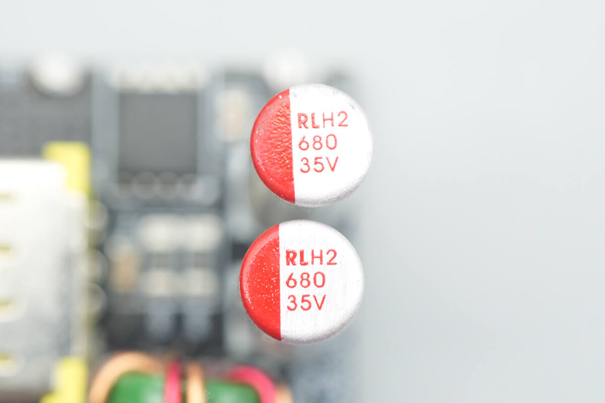
Both output solid capacitors are rated at 35V, 680μF.
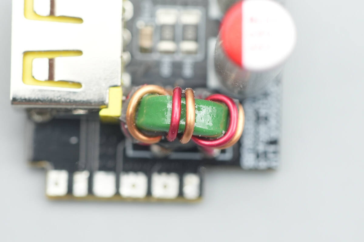
Close-up of the filter inductor.
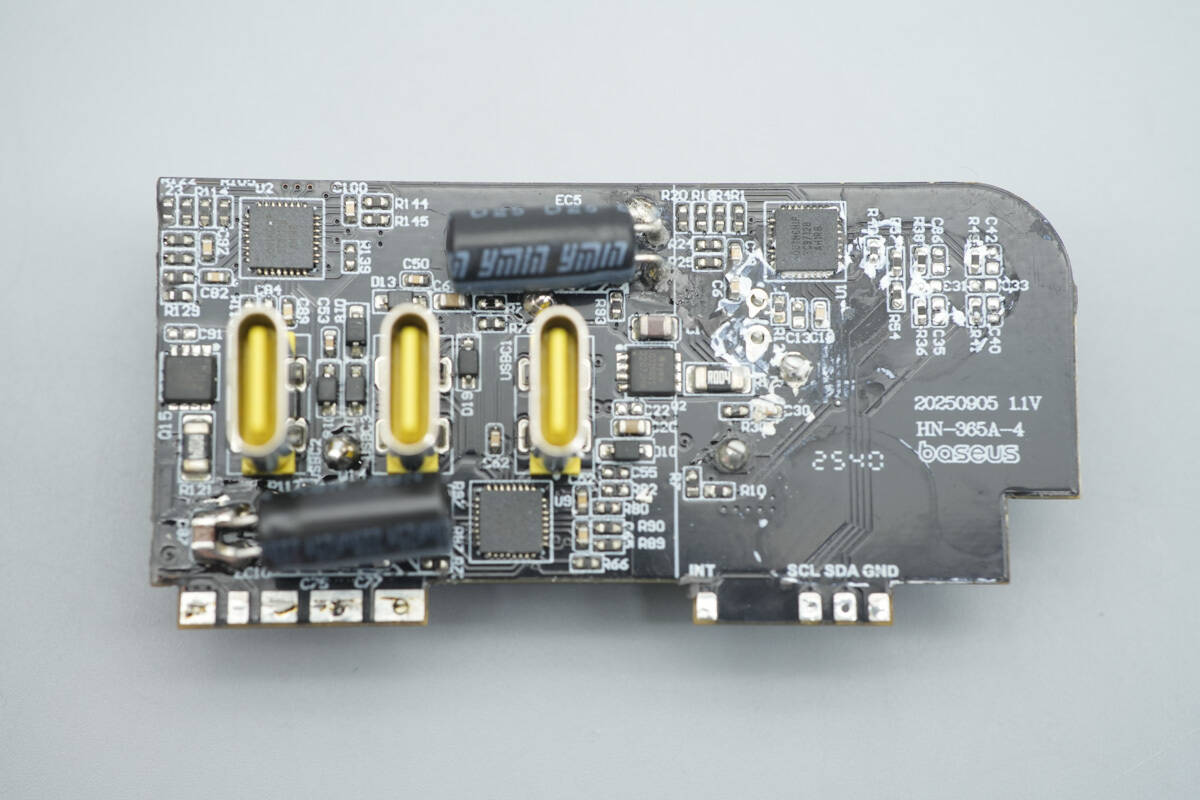
The PCB housing the USB-C socket features three secondary buck converter circuits.
The back side features buck inductors, filter capacitors, synchronous buck MOSFETs, and output VBUS MOSFETs.
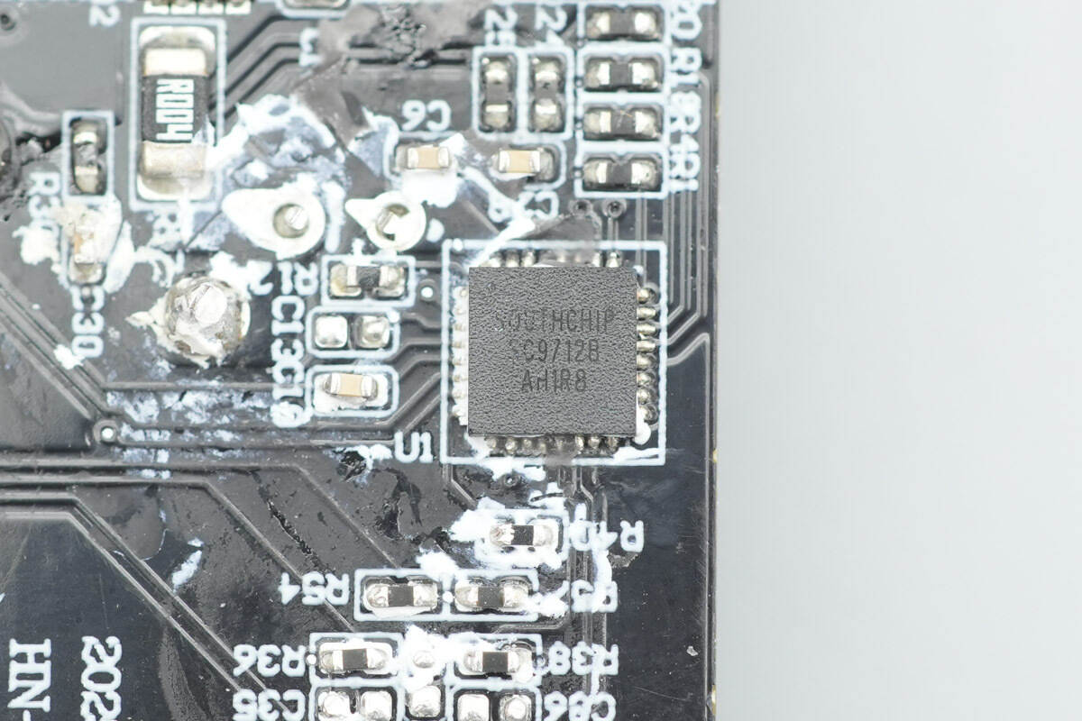
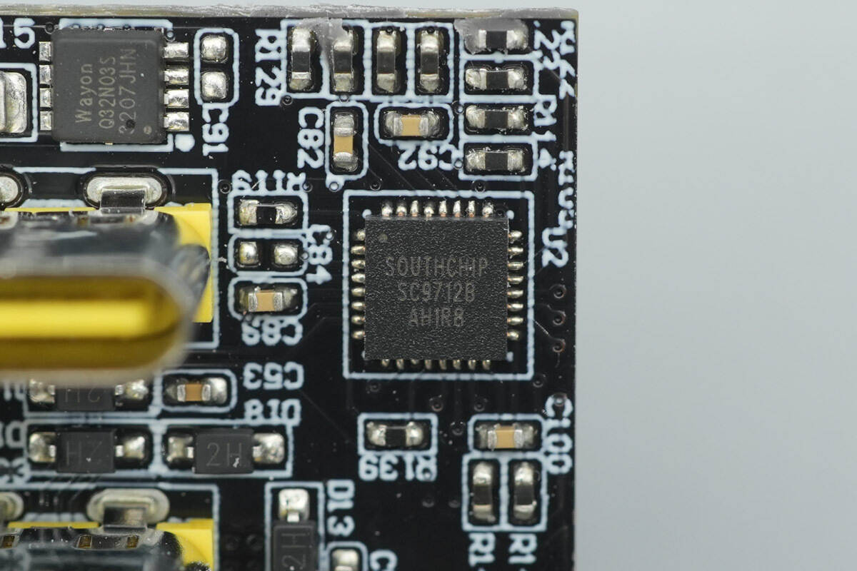
The buck protocol chip for the USB-C1 port is from SouthChip, model SC9712B. This is a highly integrated dual-port fast charging SoC that supports multiple fast charging protocols. It features a 36V efficient synchronous buck controller and includes one Type-C interface and two DPDM fast charging protocol interfaces, minimizing the need for external components. It also supports the UFCS fast charging protocol.
The SC9712B supports dual-chip cooperation, enabling dual-C port fast charging, and the 2C1A configuration requires no MCU control. Two SC9712B chips can communicate with each other, allowing full power output in single-port operation and automatic power distribution when both ports are in use.
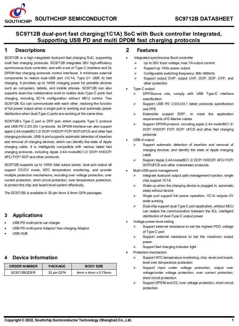
The SC9712B supports a total output power of up to 140W, with both ports supporting CC/CV modes, NTC temperature monitoring, and providing multiple protection mechanisms, including over-voltage protection, over-current protection, short-circuit protection, and over-temperature protection, effectively safeguarding the chip and system. It is housed in a 32-pin, 4×4 mm QFN package.
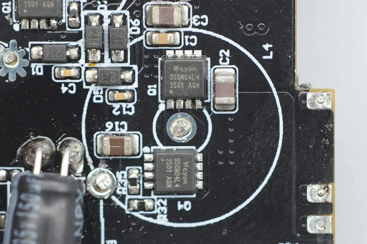
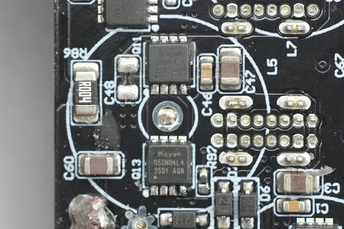
The two synchronous buck MOSFETs are from WAYON, marked with 050N04L4, and are model WMQ050N04LG2. These are NMOS with a voltage rating of 40V and an on-resistance of 5mΩ, housed in a PDFN 30×30-8L package.

The buck protocol chip for the USB-C2 port is also the SouthChip SC9712B.
The two synchronous buck MOSFETs paired with the USB-C2 port are also WAYON WMQ050N04LG2.
The buck protocol chip for the USB-C3 and USB-A ports is also SouthChip SC9712B.
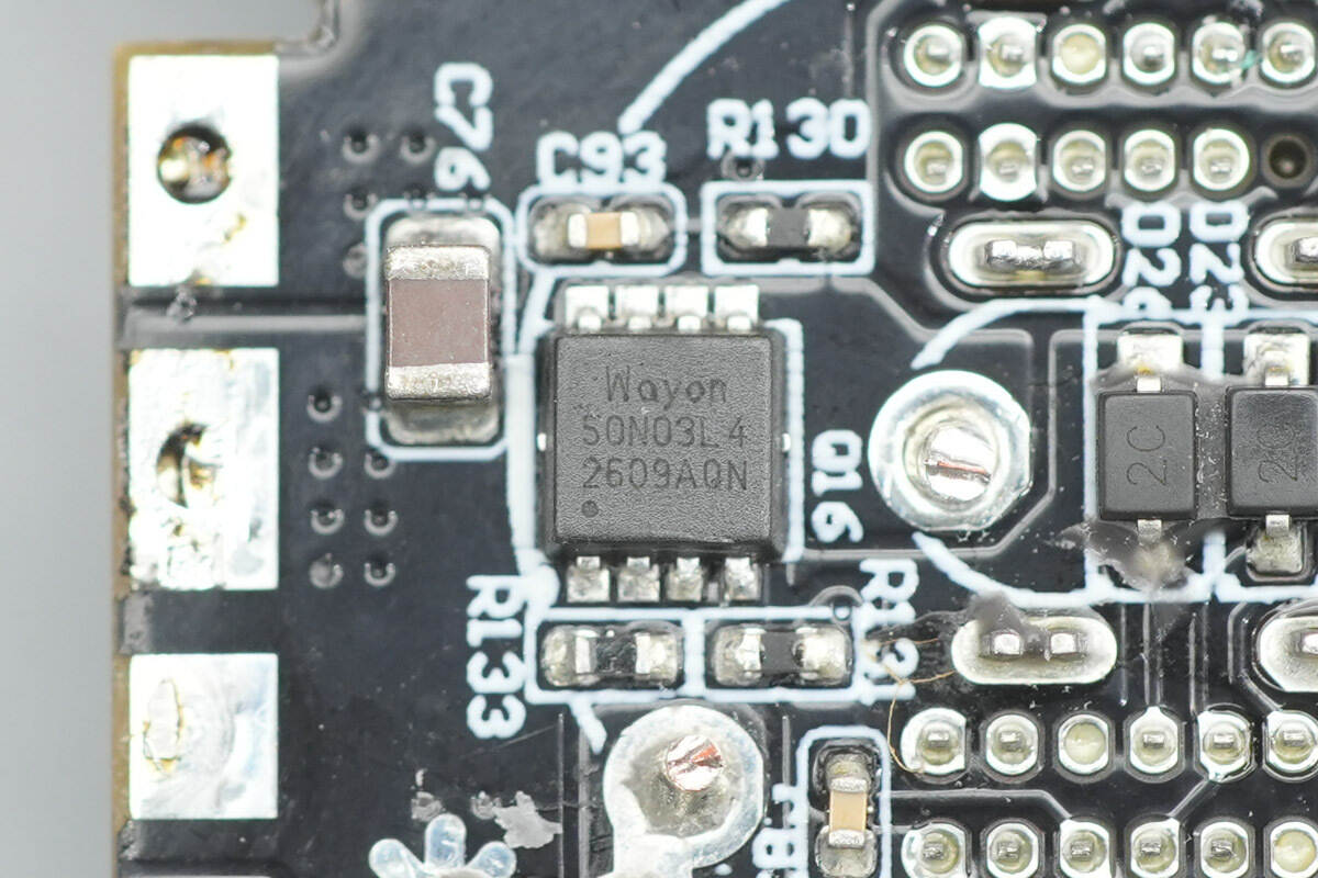
The synchronous buck MOSFETs paired with the USB-C3 and USB-A ports are from WAYON, marked with 50N03L4, and are model WMQ050N03LG4. These are NMOS with a voltage rating of 30V and an on-resistance of 5.4mΩ, housed in a PDFN 30×30-8L package.
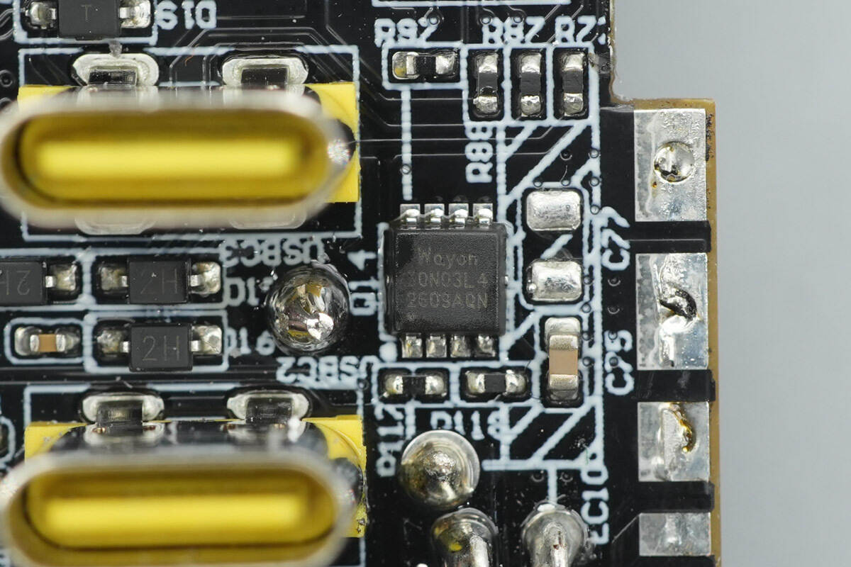
The other WAYON WMQ050N03LG4 synchronous buck MOSFET is laid out on the front side of the small PCB.
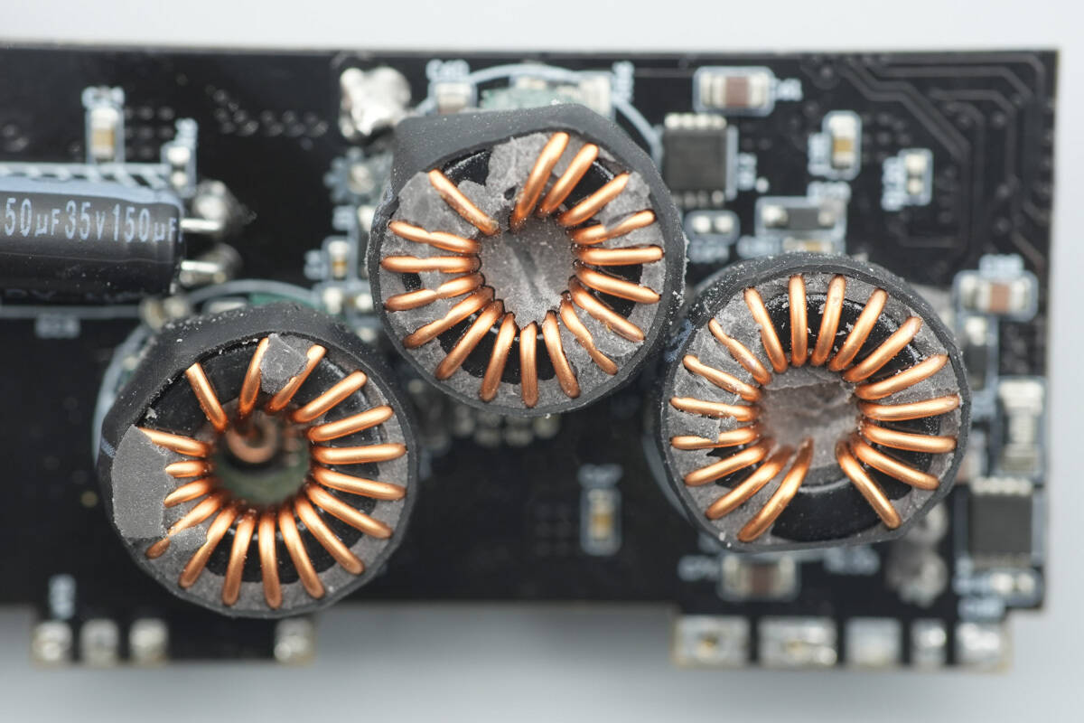
The buck inductors are all covered with heat shrink tubing for insulation protection.
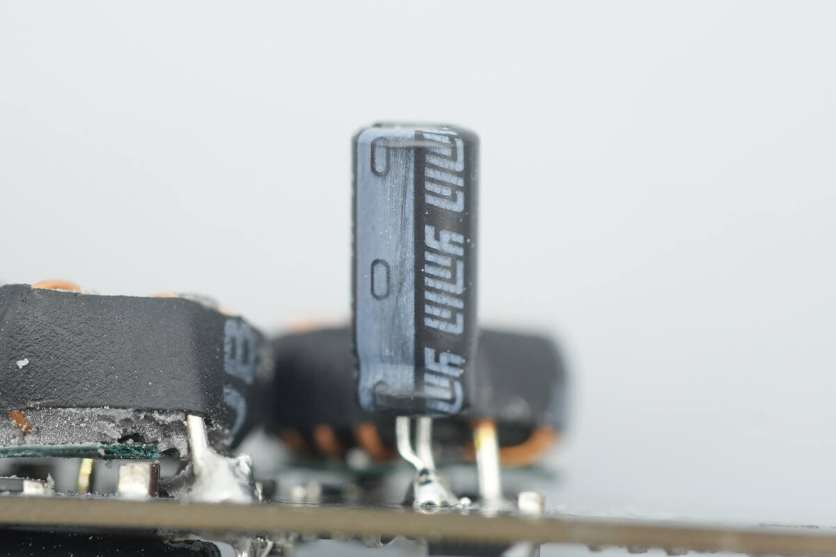
The buck output filter solid capacitors are all from YMIN.
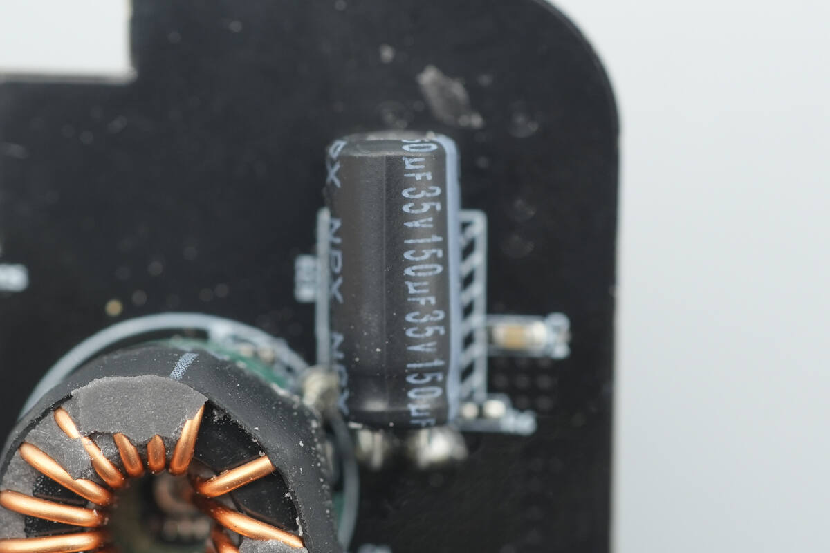
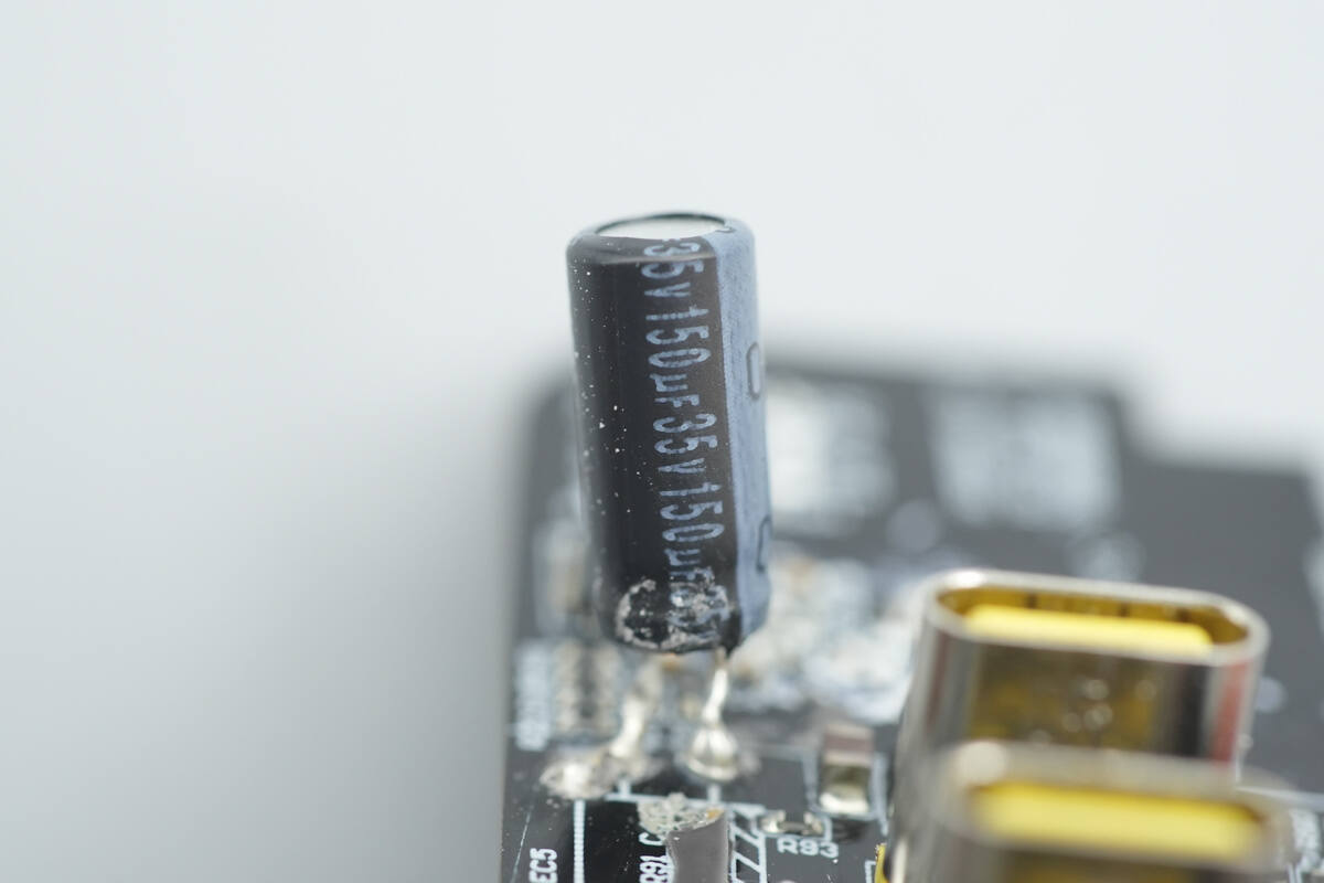
The three capacitors are all from the NPX high-capacity density series. The capacitor used for the USB-C1 port's buck output filtering is rated at 35V, 150μF.
The capacitor used for the USB-C2 port is also rated at 35V, 150μF.
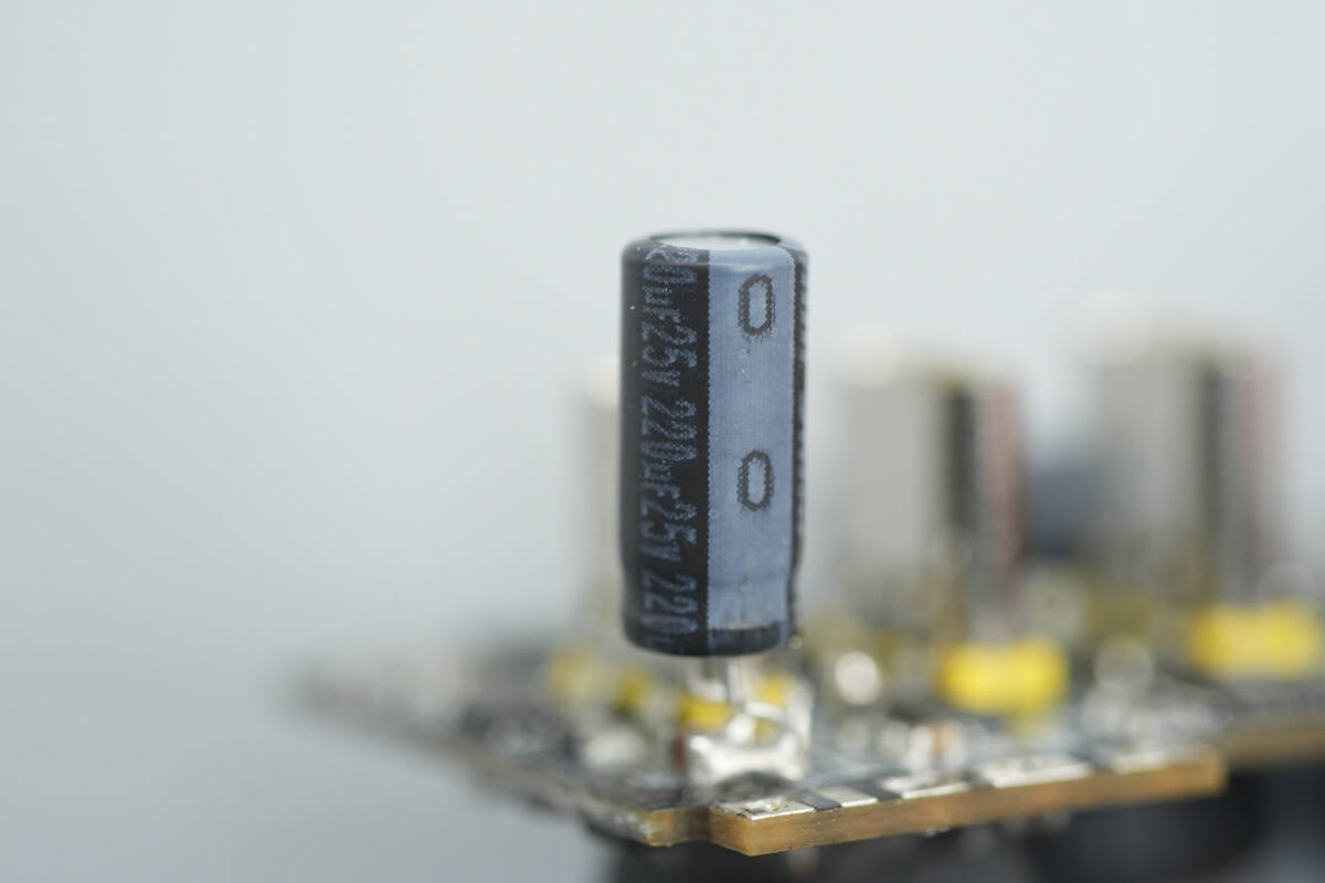
The capacitor used for the USB-C3 and USB-A ports is rated at 25V, 220μF.
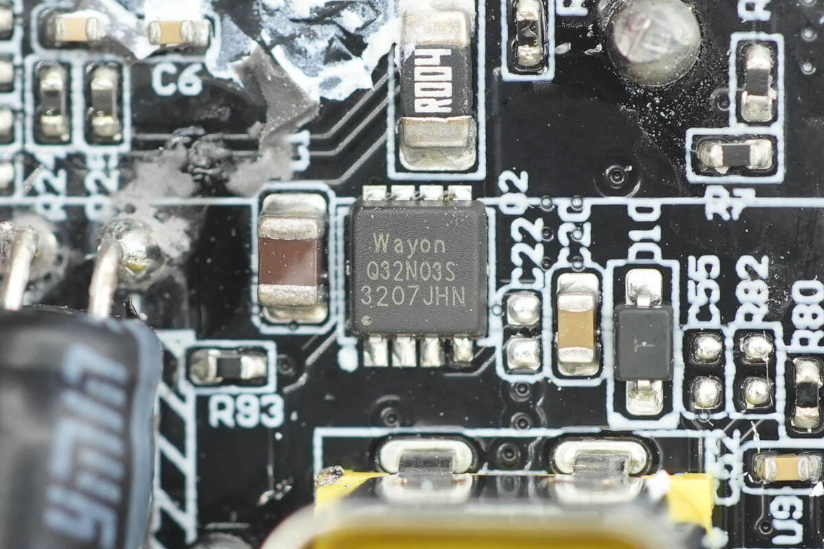
The output VBUS MOSFET for the USB-C1 port is from WAYON, model WMQ32N03TS. It is an NMOS with a voltage rating of 30V and an on-resistance of 9mΩ, housed in a PDFN 30×30-8L package.
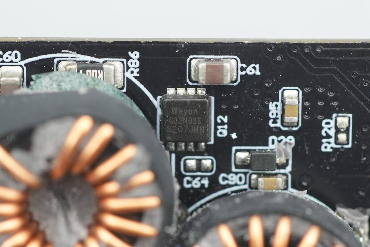
The output VBUS MOSFET for the USB-C2 port is also the WAYON WMQ32N03TS.
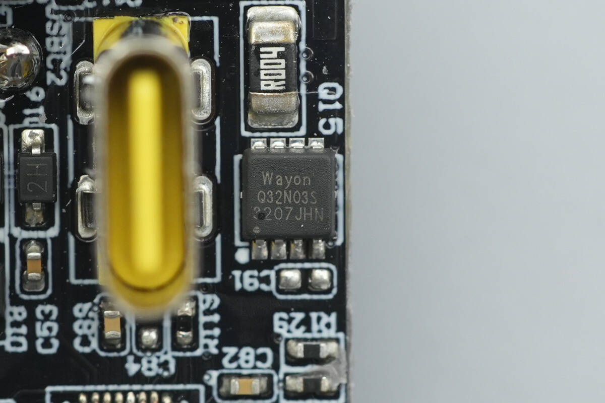
The output VBUS MOSFET for the USB-C3 port is also the WAYON WMQ32N03TS.
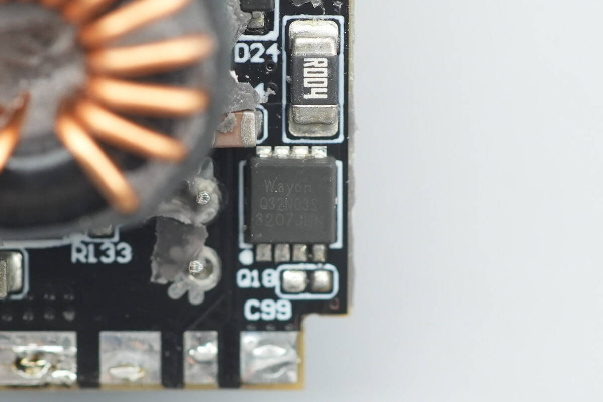
The output VBUS MOSFET for the USB-A port is also the WAYON WMQ32N03TS.
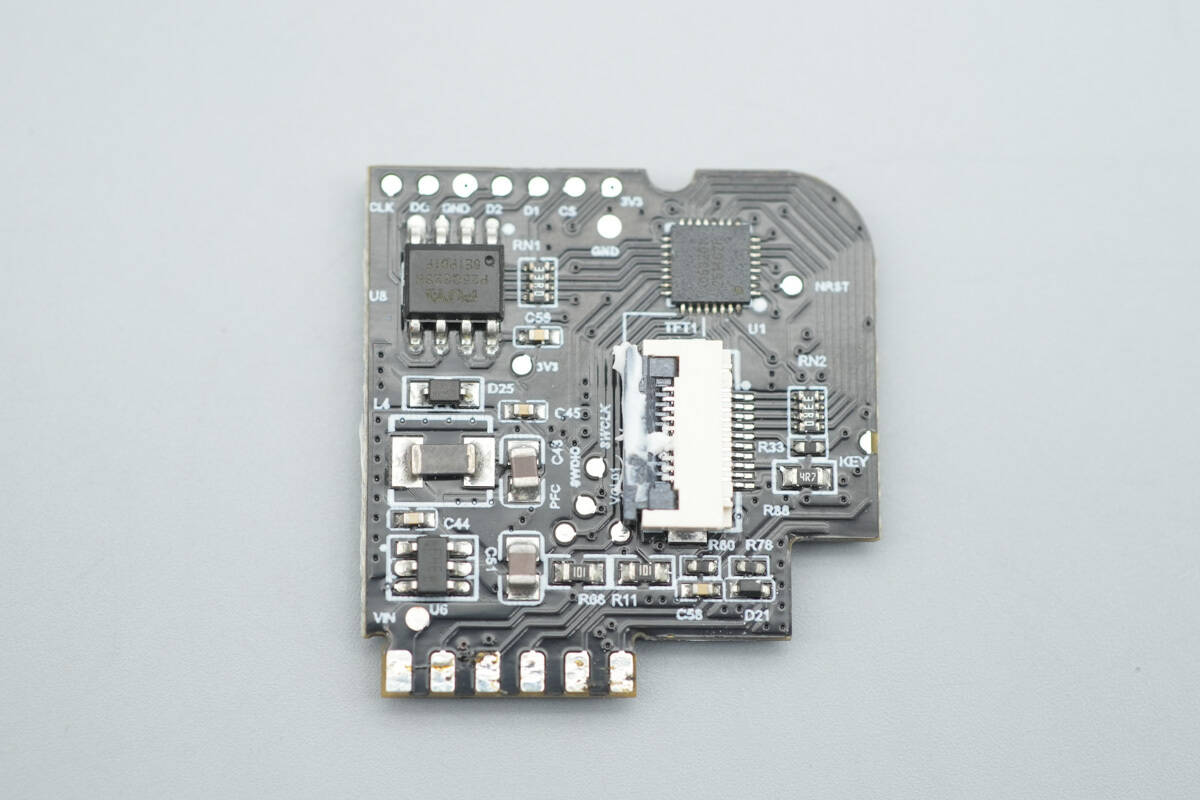
The front side of the display control PCB features components such as the MCU, memory, and other devices.
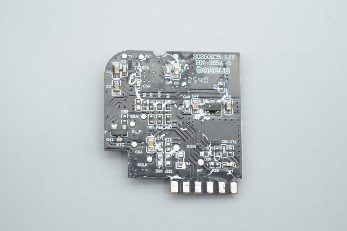
The back side overview.
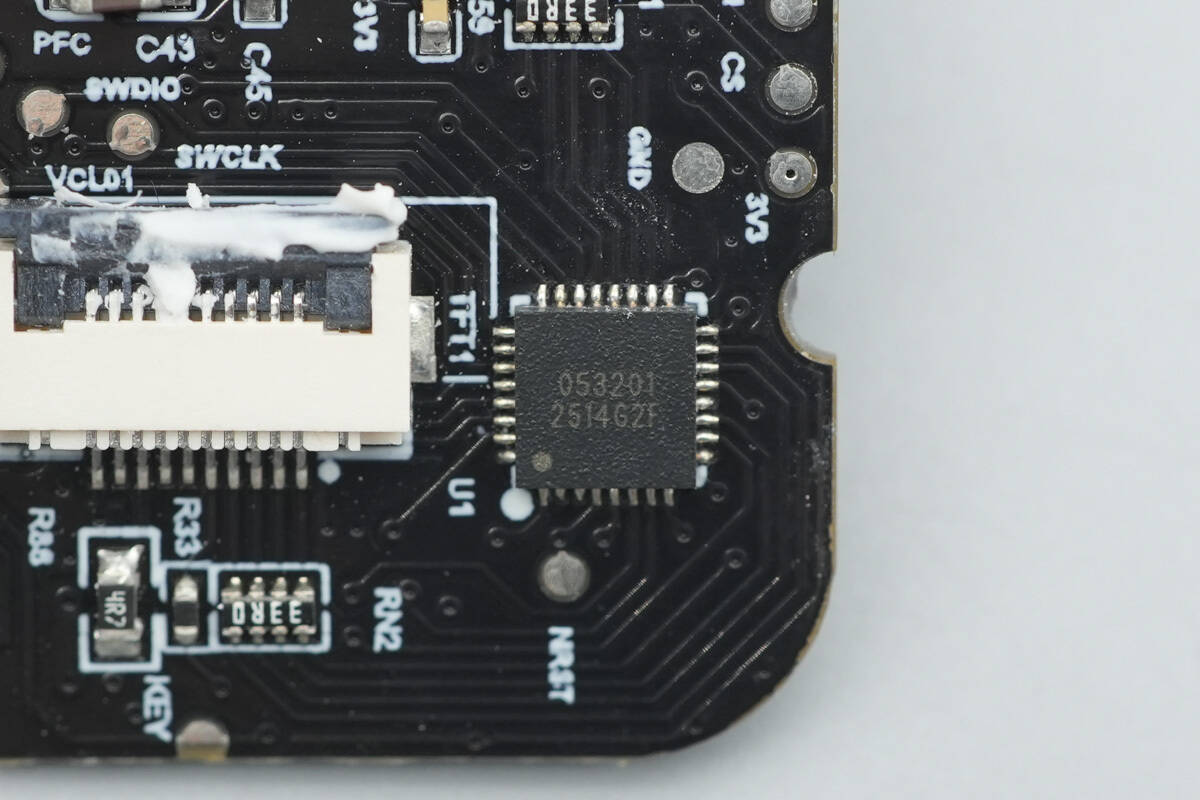
The MCU used for screen control is marked with 053201 and comes in a QFN32 package.
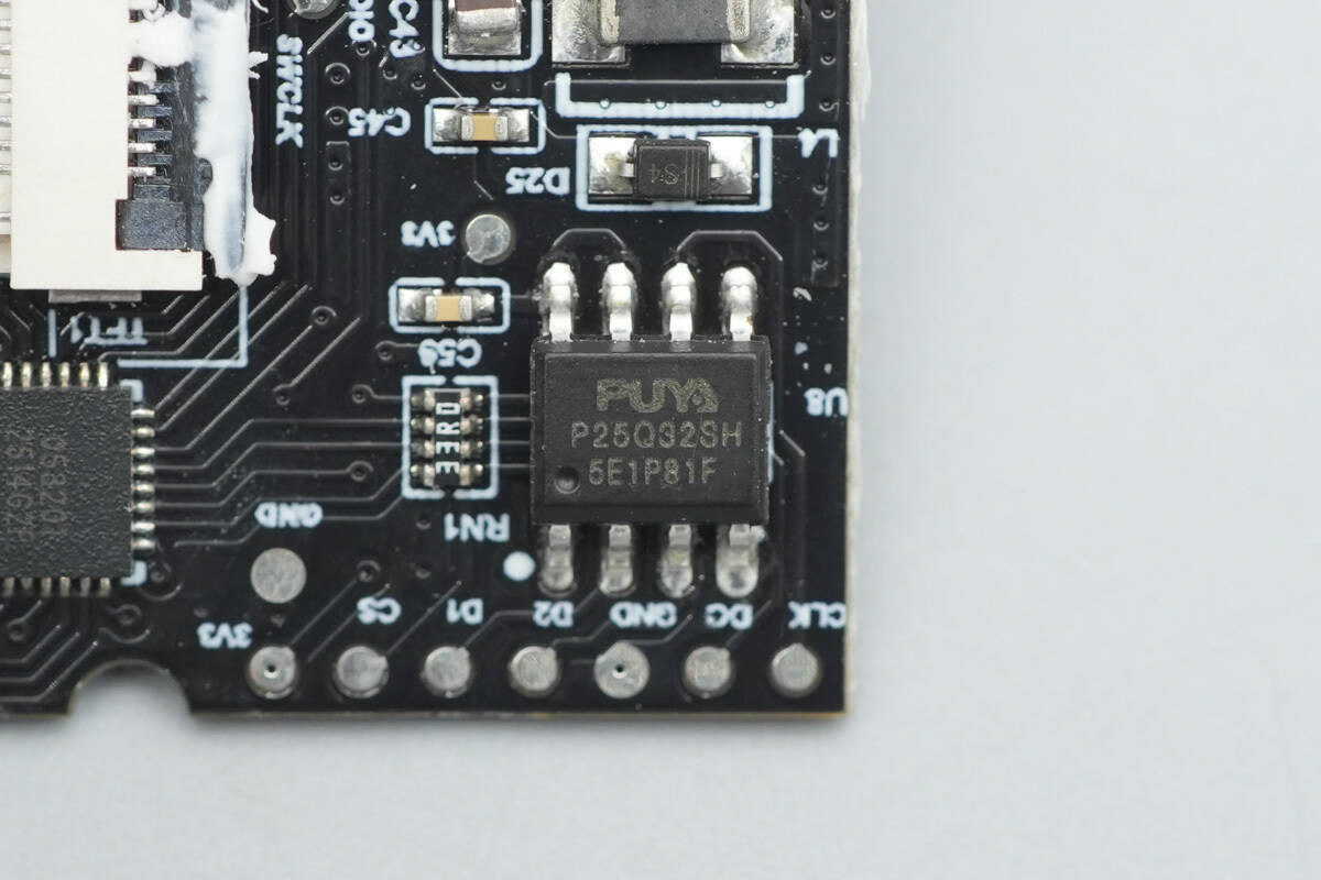
The memory is from Puya, model P25Q32SH. It is a serial interface flash memory device, specifically designed for high-volume consumer applications. The device features a flexible erase architecture, and its page-erase granularity makes it highly suitable for data storage, eliminating the need for additional storage devices.
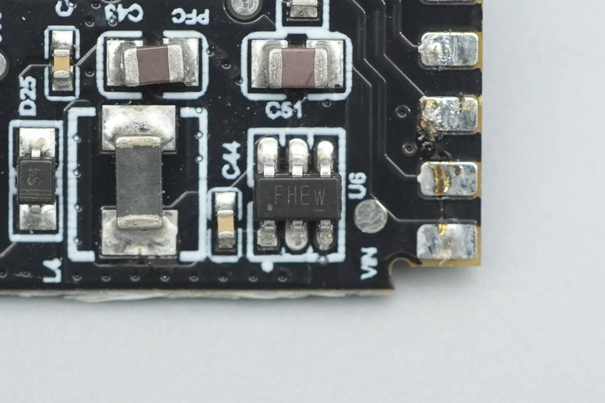
One of the chips is from ETA, marked with "FH," and is housed in a SOT23-6 package.

Well, those are all components of the Baseus PicoGo AH11 140W GaN Fast Charger.
Summary of ChargerLAB
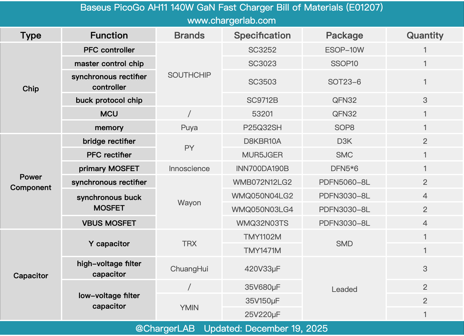
Here is the component list of the Baseus PicoGo AH11 140W GaN Fast Charger for your convenience.
Its smart display not only supports mainstream Windows but also provides more detailed information, such as output voltage, current, and other parameters for each interface. The three USB-C ports and one USB-A port are compatible with PD3.1/PPS, SCP, and other protocols, allowing simultaneous charging of devices such as laptops, tablets, smartphones, and headphones.
After taking it apart, we found that it uses the full fast charging power solution from SouthChip, including the SC3252, SC3023, SC3503, and SC9712B, paired with Innoscience's INN700DA190B GaN device and several power devices from WAYON. The PCBA module is encapsulated with resin to enhance heat dissipation and weather resistance.
Related Articles:
1. Teardown of GreatWall 3000W Platinum CRPS Power Supply (GW-CRPS3000L5R)
2. Teardown of Belkin BoostCharge Pro Dual USB-C 67W GaN Wall Charger (WCH020yz)
3. Teardown of Huntkey 140W GaN Charger (HKC14028050-0B1)