Introduction
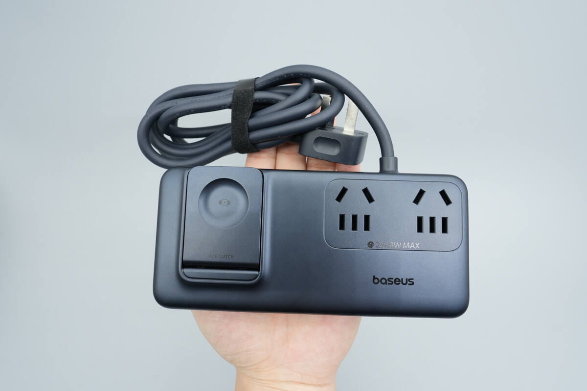
Baseus has introduced a 7-in-1 100W charging station that has passed Huawei’s official protocol certification, supporting Huawei 66W SuperCharge and wireless charging for Huawei smartwatches. It features two AC power sockets and adopts an independent, strong-and-weak-current partitioned architecture, along with surge protection to ensure safe power usage.
The charging station is also equipped with two USB-C ports and one USB-A port, a 1-meter braided retractable cable, and a built-in wireless charging pad for smartwatches. Either USB-C port supports up to 100W output and features automatic power distribution, enabling fast charging for a smartphone and a laptop simultaneously. Below, we take a closer look at the detailed design of the product.
Product Appearance
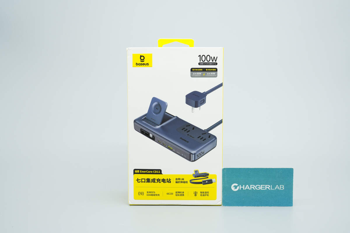
The front of the packaging box displays the Baseus brand, the product appearance, output power, product name, and key selling points.
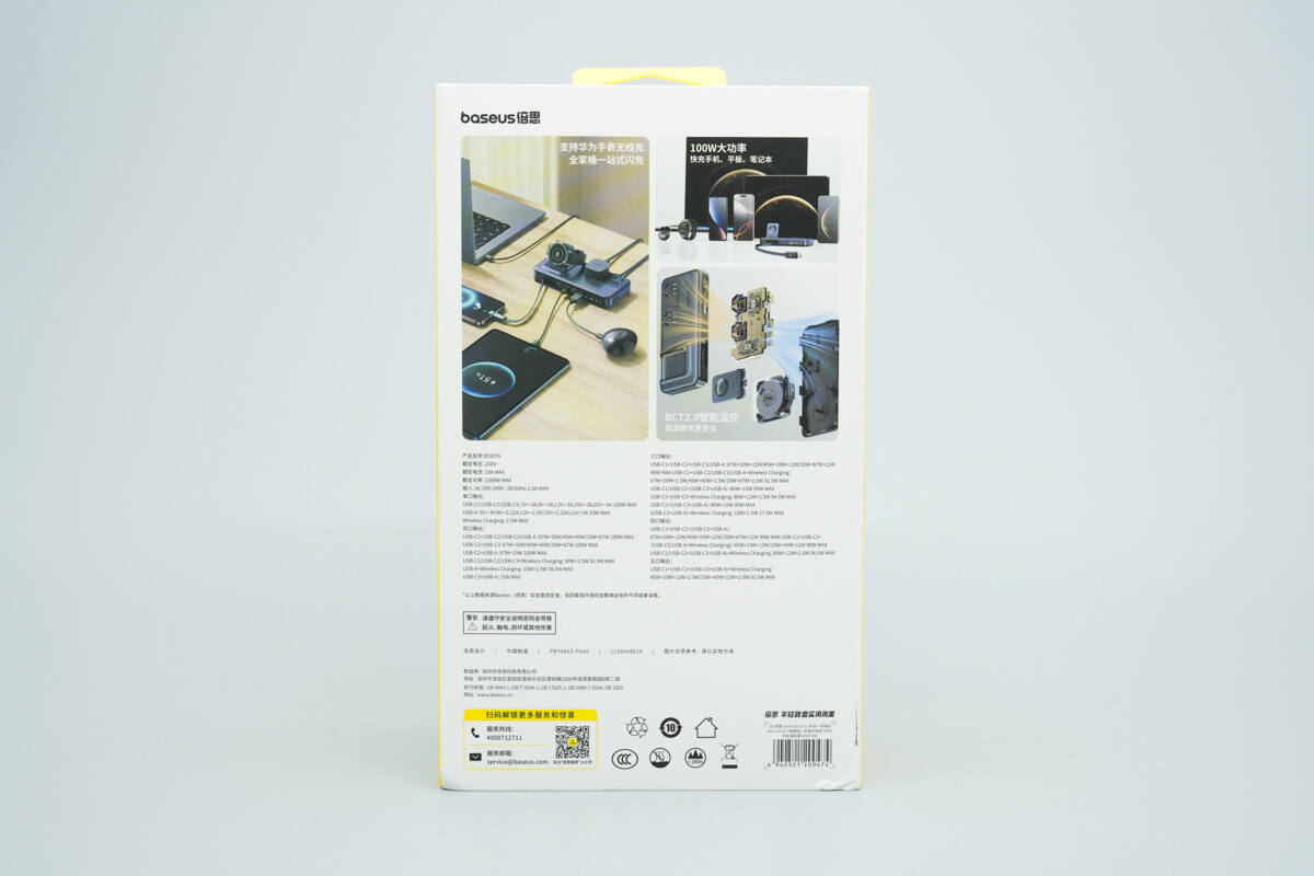
The back of the packaging box shows product usage scenarios and technical specifications.
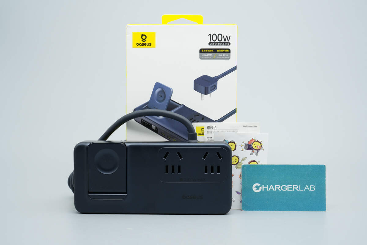
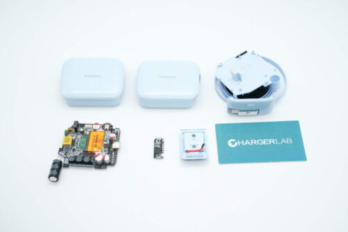
The package includes the charging station, a user manual, stickers, and other accessories.
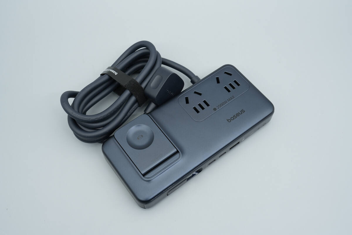
It comes with a built-in three-prong AC power cord with a conductor cross-section of 1.5 mm², and the main unit features a flat, elongated rectangular form factor.
It comes with a built-in three-prong AC power cord with a conductor cross-section of 1.5 mm², and the main unit features a flat, elongated rectangular form factor.
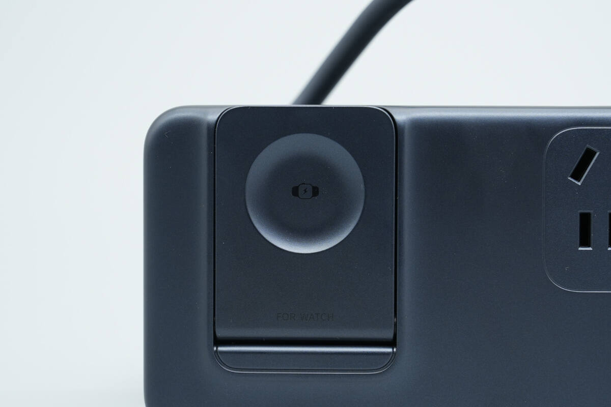
The wireless charging module supports adjustable angles and can be freely positioned at different tilt angles.
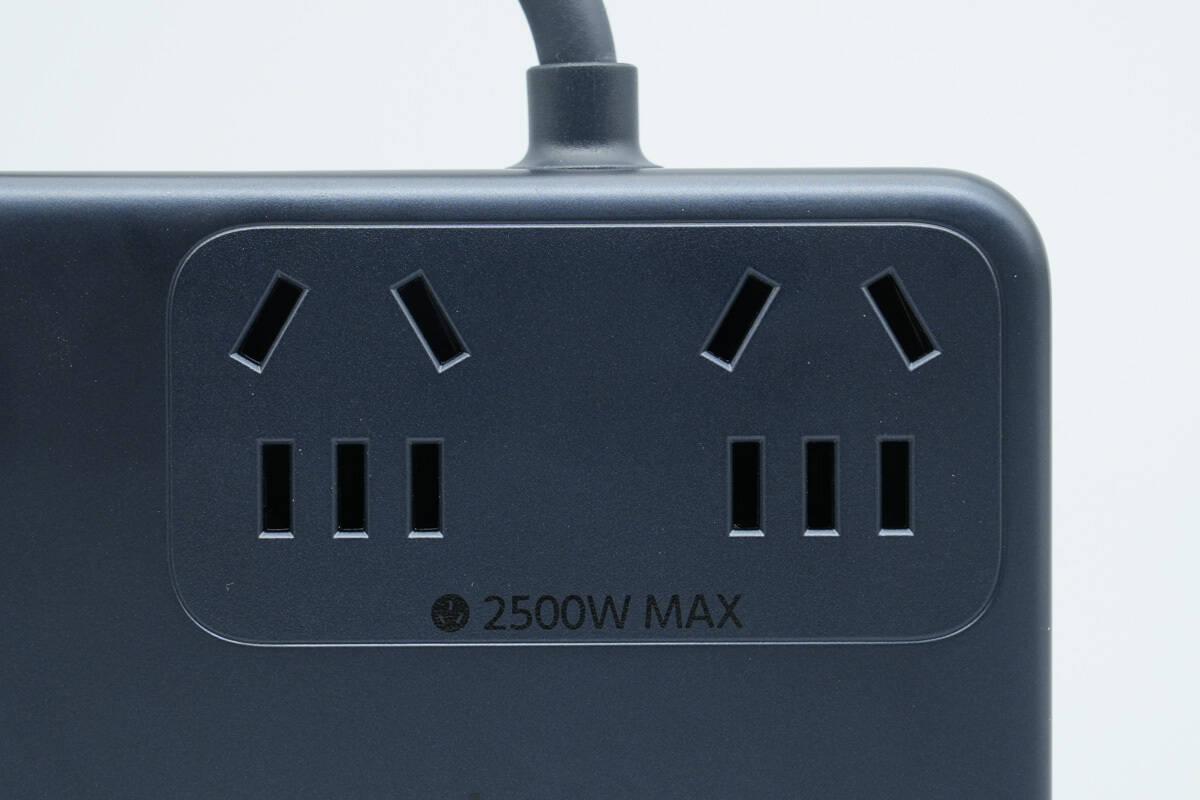
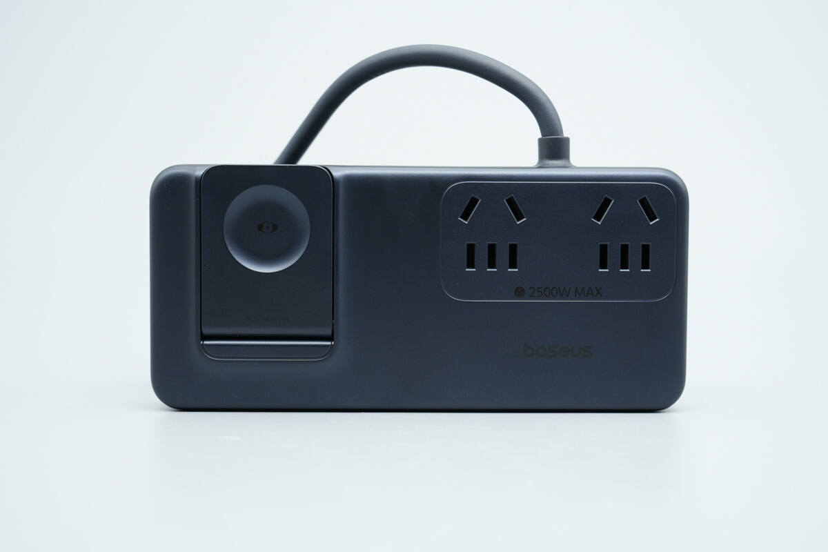
Close-up of the two five-hole AC power sockets.
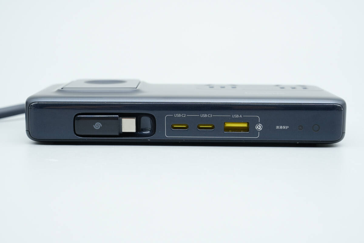
The front of the unit features a retractable USB-C cable, along with two USB-C ports and a USB-A port, while the right side is equipped with a surge protection indicator.
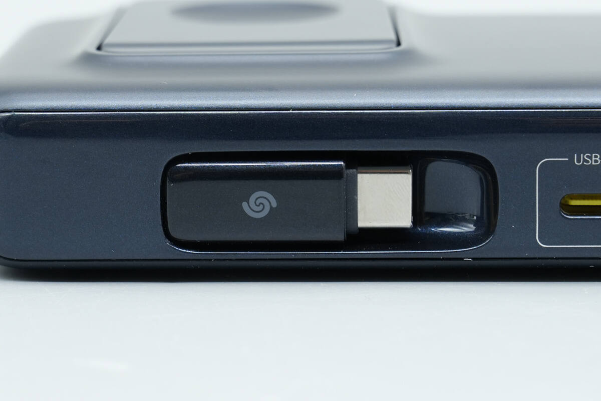
The retractable cable connector is made of a zinc-alloy housing.
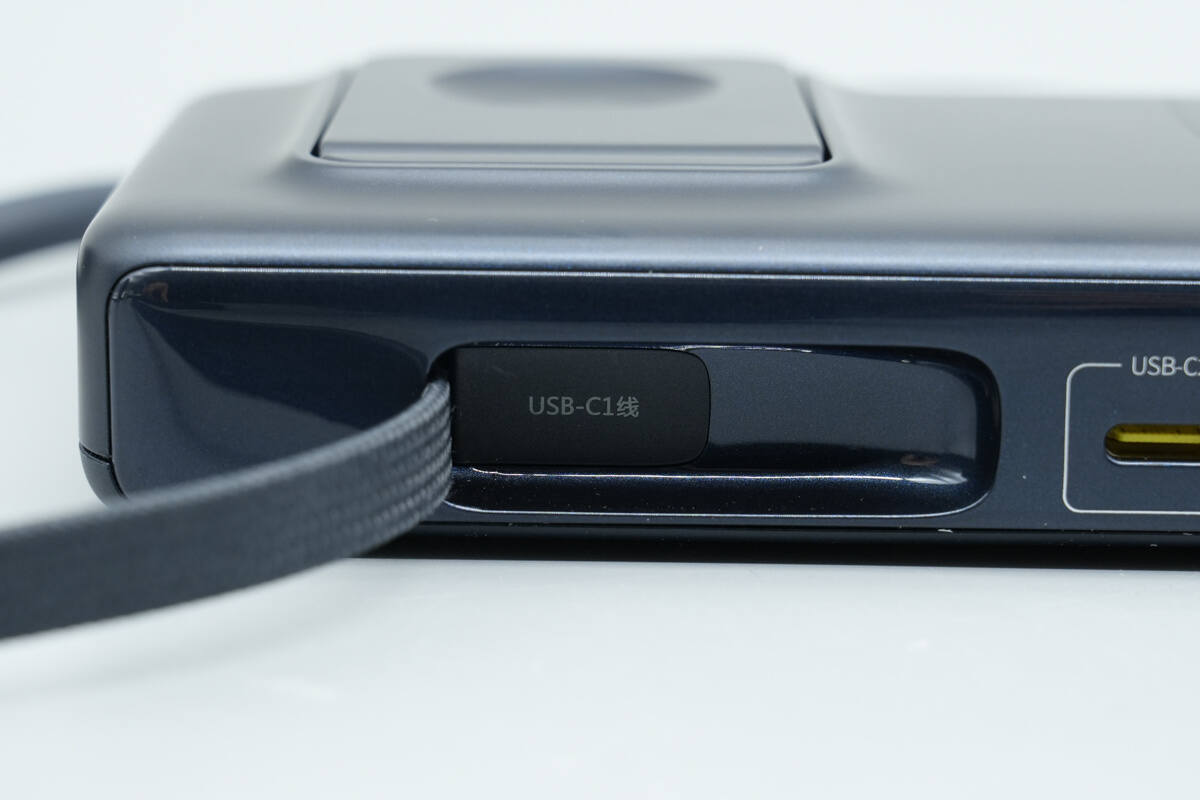
It features magnetic attachment for secure placement and is made of braided material.
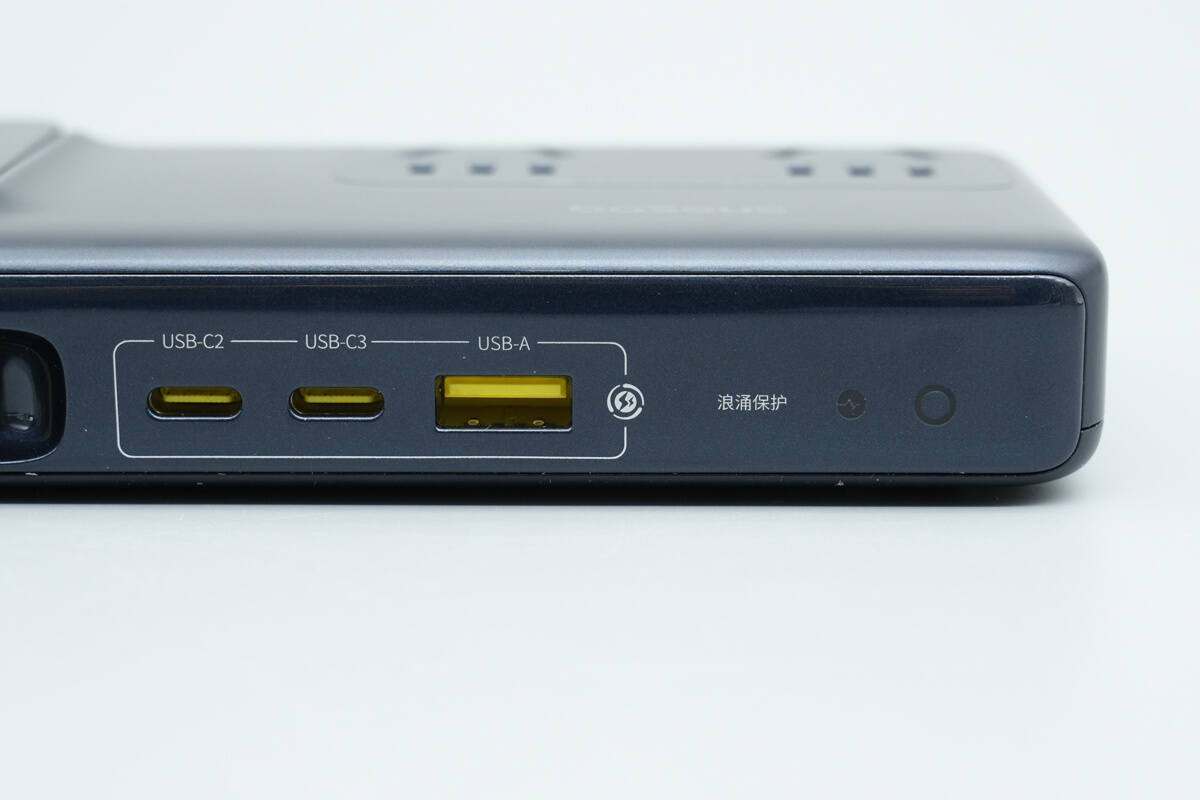
The plastic sheets of USB-C and USB-A ports are yellow.
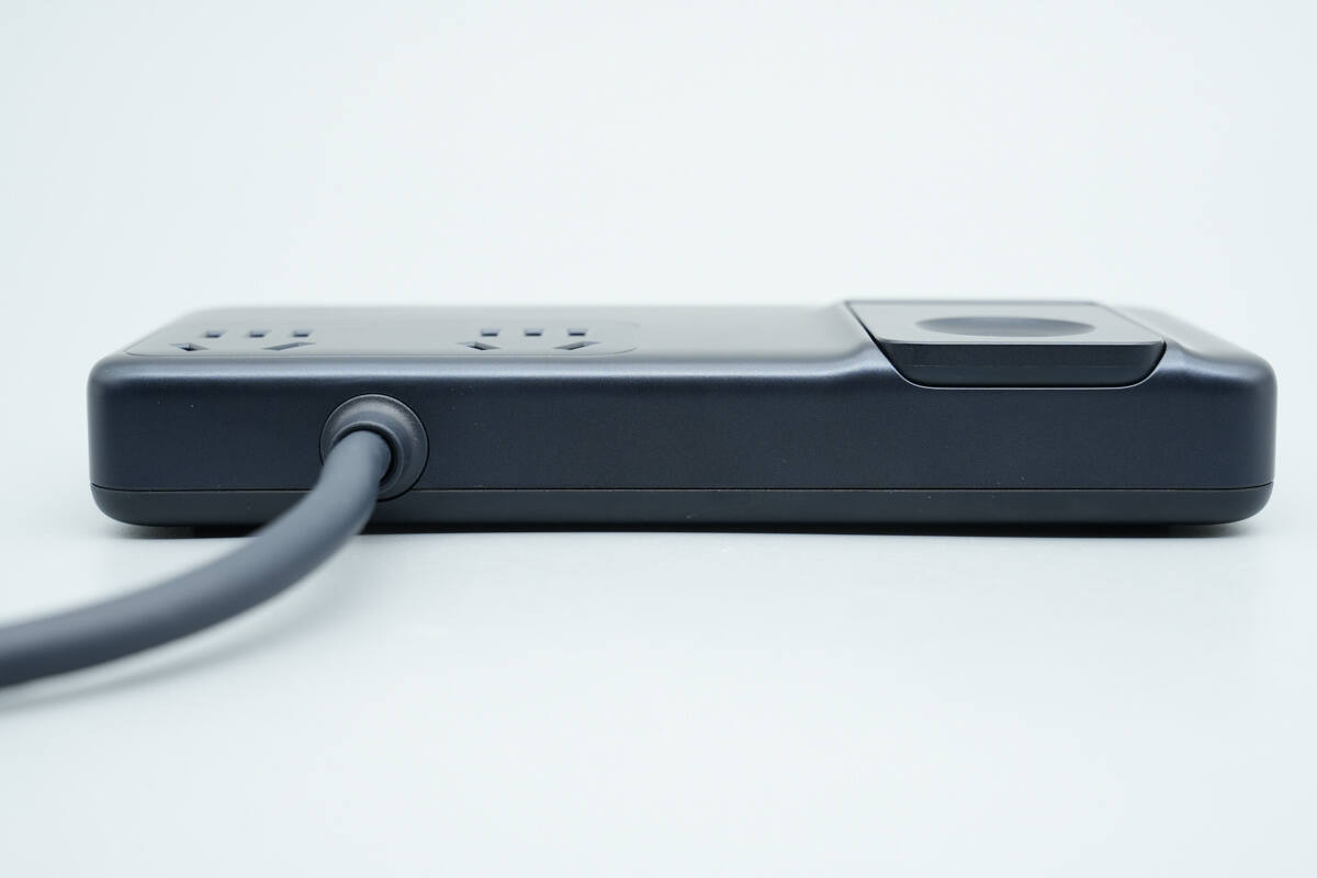
The rear of the unit is equipped with the power cord.
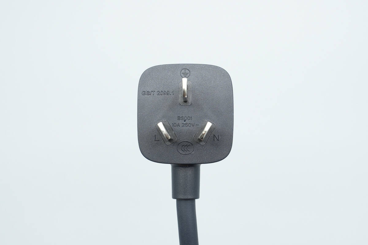
Close-up of the three-prong plug.
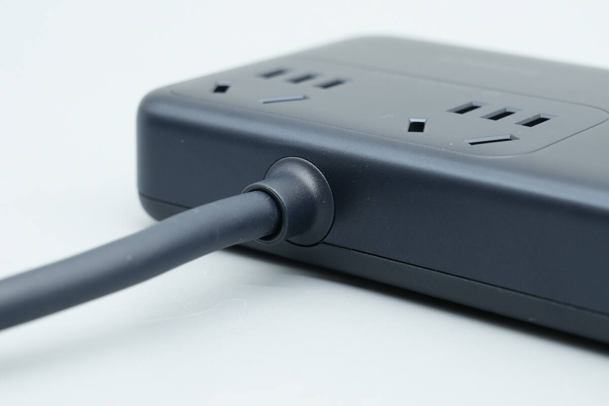
The junction between the power cord and the main unit is fitted with a protective rubber sleeve to prevent bending and enhance durability.
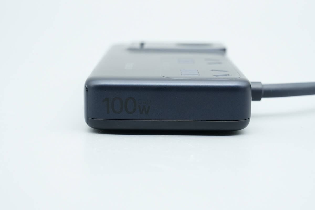
The side of the unit is labeled with the 100W output power.
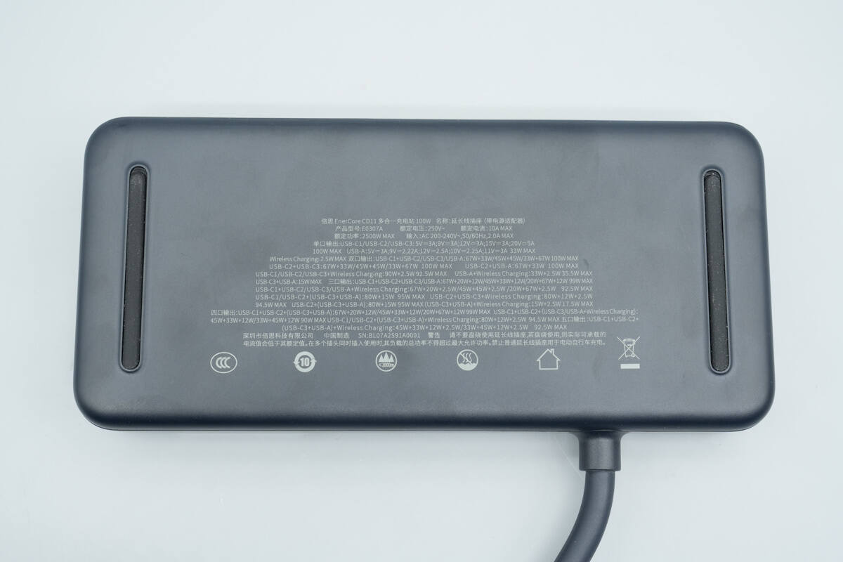
The bottom of the unit features anti-slip pads on both sides and displays product information.
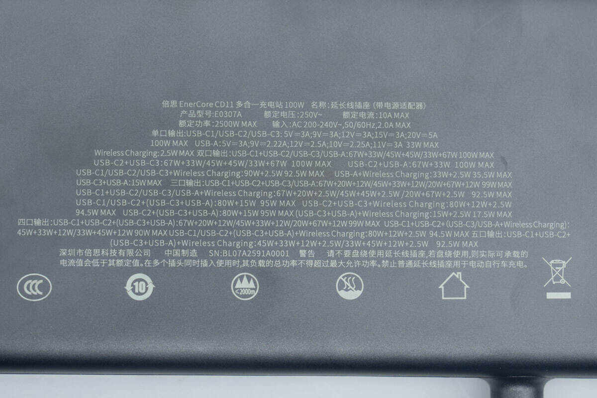
Baseus EnerCore CD11 Multi-functional Charging Station 100W
Name: Extension Socket (with Power Adapter)
Model: E0307A
Rated Voltage: 250V~
Rated Current: 10A MAX
Rated Power: 2500W MAX
Input: AC 200-240V~, 50/60Hz, 2.0A MAX
Single-port Output:
USB-C1/C2/C3: 5V 3A, 9V 3A, 12V 3A, 15V 3A, 20V 5A, 100W MAX
USB-A: 5V 3A, 9V 2.22A, 12V 2.5A, 10V 2.25A, 11V 3A, 33W MAX
Wireless Charging: 2.5W MAX
Dual-port Output:
C1 + C2/C3/USB-A: 67W + 33W / 45W + 45W / 33W + 67W, 100W MAX
C2 + C3: 67W + 33W / 45W + 45W / 33W + 67W, 100W MAX
C2 + USB-A: 67W + 33W, 100W MAX
C1/C2/C3 + Wireless Charging: 90W + 2.5W, 92.5W MAX
USB-A + Wireless Charging: 33W + 2.5W, 35.5W MAX
C3 + USB-A: 15W MAX
Three-port Output:
C1 + C2 + C3/USB-A: 67W + 20W + 12W / 45W + 33W + 12W / 20W + 67W + 12W, 99W MAX
C1 + C2/C3/USB-A + Wireless Charging: 67W + 20W + 2.5W / 45W + 45W + 2.5W / 20W + 67W + 2.5W, 92.5W MAX
C1 + C2 + (C3 + USB-A): 80W + 15W, 95W MAX
C2 + C3 + Wireless Charging: 80W + 12W + 2.5W, 94.5W MAX
C2 + (C3 + USB-A): 80W + 15W, 95W MAX
(C3 + USB-A) + Wireless Charging: 15W + 2.5W, 17.5W MAX
Four-port Output:
C1 + C2 + (C3 + USB-A): 67W + 20W + 12W / 45W + 33W + 12W / 20W + 67W + 12W, 99W MAX
C1 + C2 + (C3/USB-A + Wireless Charging): 45W + 33W + 12W / 33W + 45W + 12W, 90W MAX
C1/C2 + (C3 + USB-A + Wireless Charging): 80W + 12W + 2.5W, 94.5W MAX
Five-port Output:
C1 + C2 + (C3 + USB-A) + Wireless Charging: 45W + 33W + 12W + 2.5W / 33W + 45W + 12W + 2.5W, 94.5W MAX
The product has obtained CCC certification.
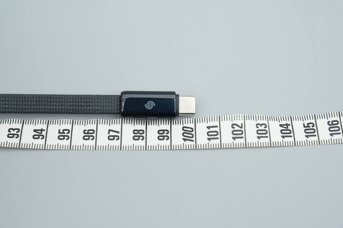
The length of the retractable cable is about 1 m (39.37 inches).
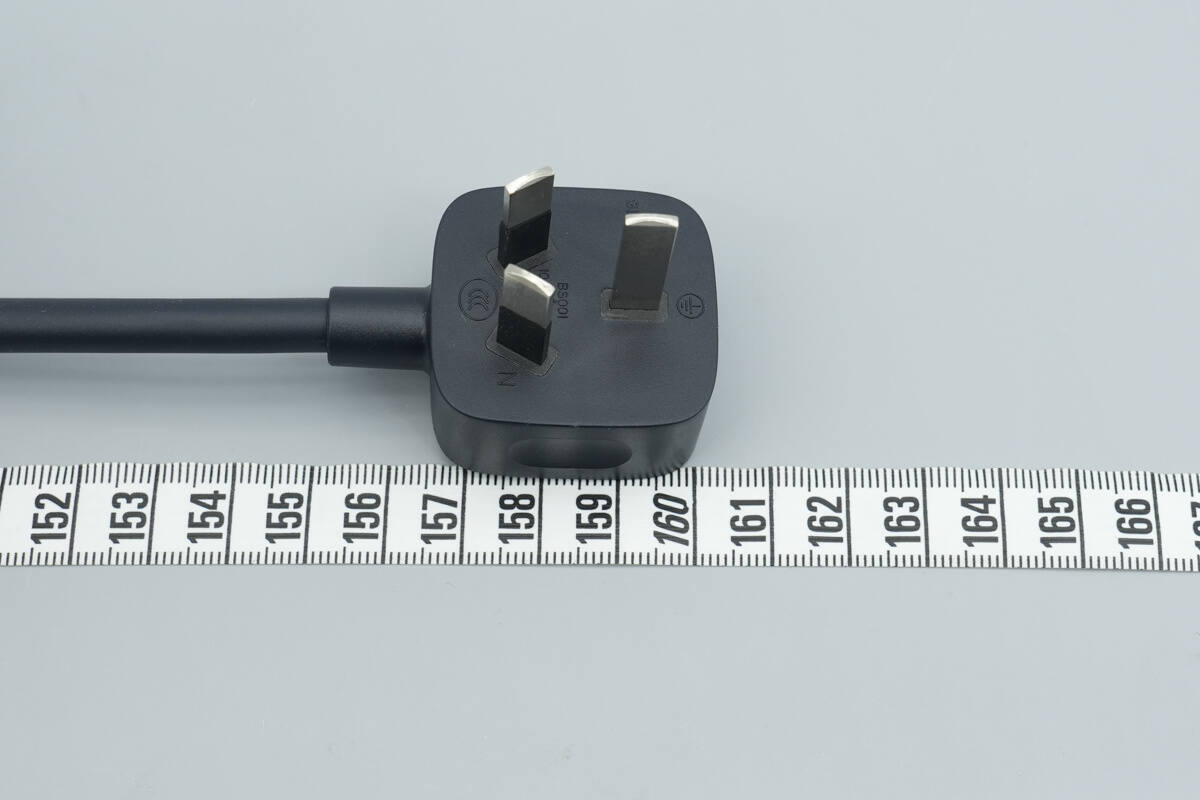
The length of the power cord is about 160 cm (63 inches).
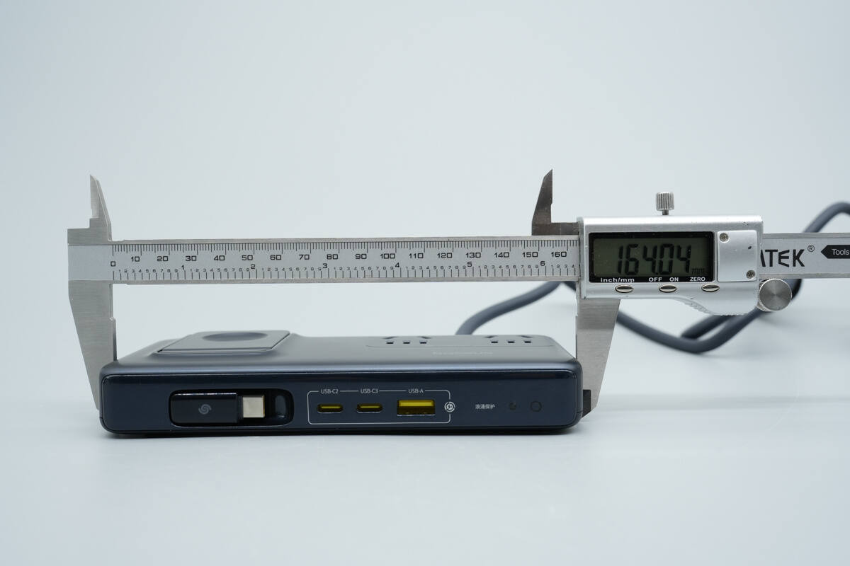
The length of the charging station is about 164 mm (6.46 inches).
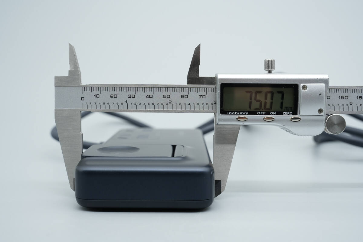
The width is about 75.1 mm (2.96 inches).
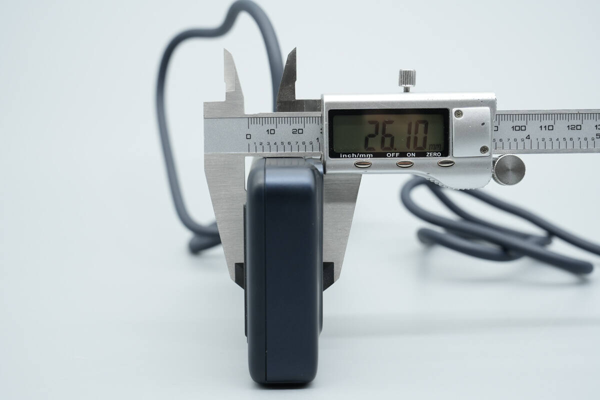
The thickness is about 26.1 mm (1.028 inches).
That's how big it is on the hand.
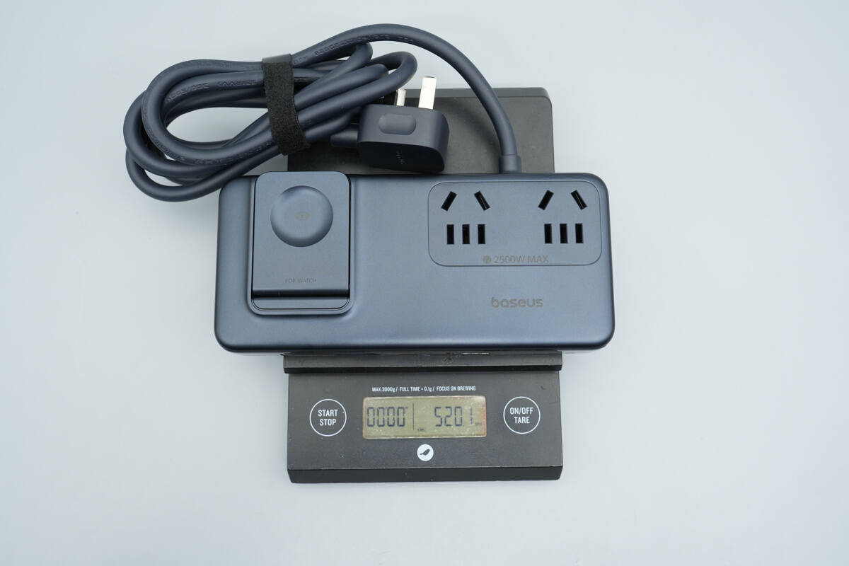
The weight is about 520 g (18.34 oz).
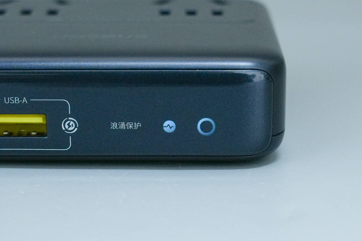
When the charging station is connected to the power supply, the surge protection and power indicator lights turn on.
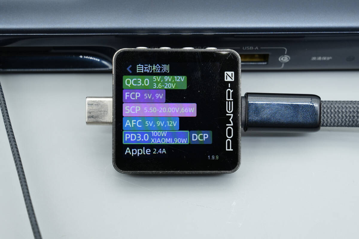
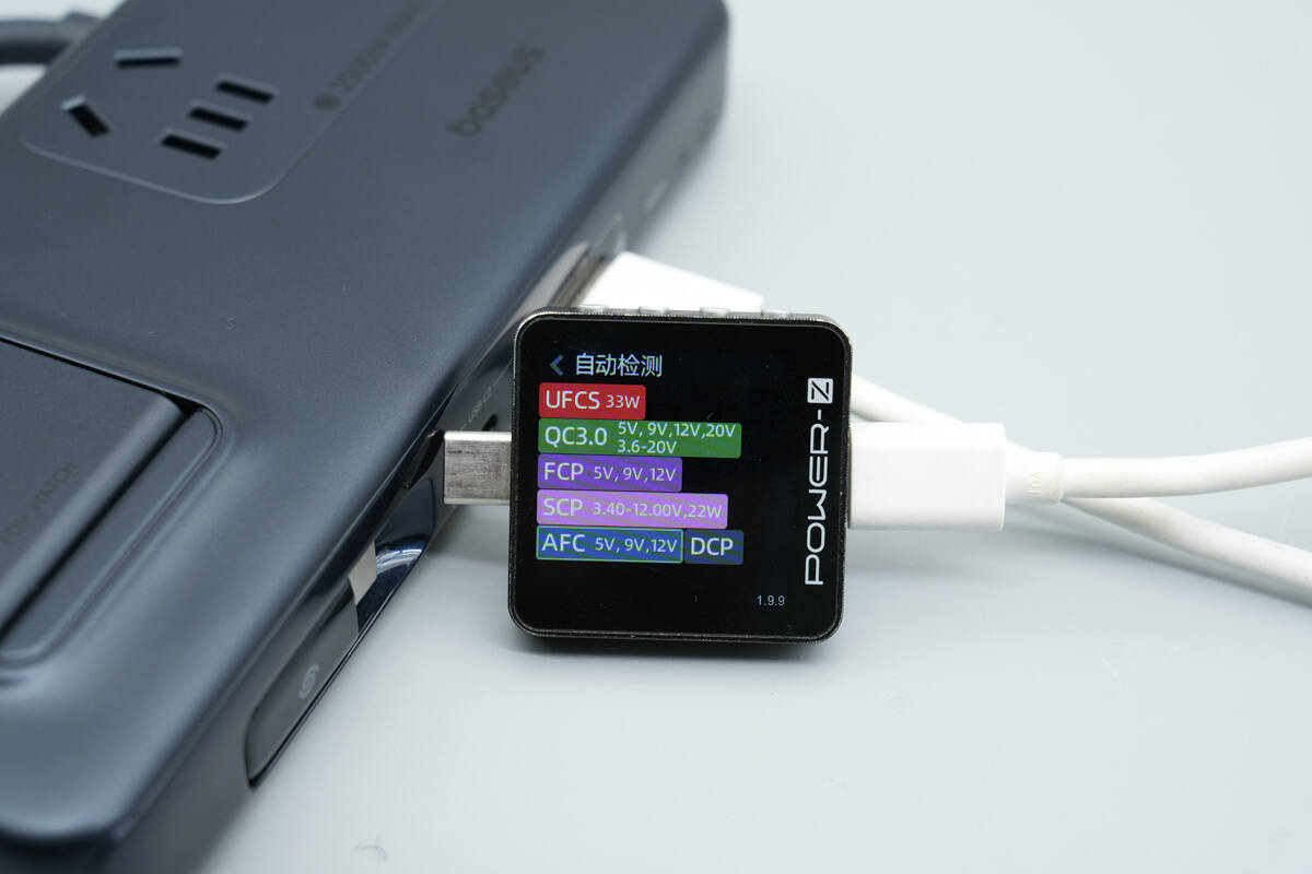
ChargerLAB POWER-Z KM003C shows that the USB-C cable supports QC3.0, FCP, SCP, AFC, PD3.0, DCP, and Apple 2.4A charging protocols, and also supports Xiaomi’s 90W proprietary fast-charging protocol.
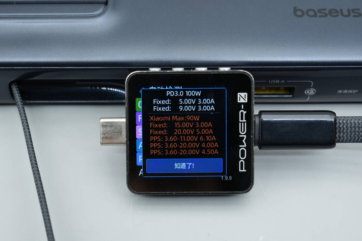
It features four fixed PDOs of 5V 3A, 9V 3A, 15V 3A, and 20V 5A, as well as three Xiaomi proprietary PPS voltage levels: 3.6–11V 6.1A, 3.6–20V 4A, and 3.6–20V 4.5A.
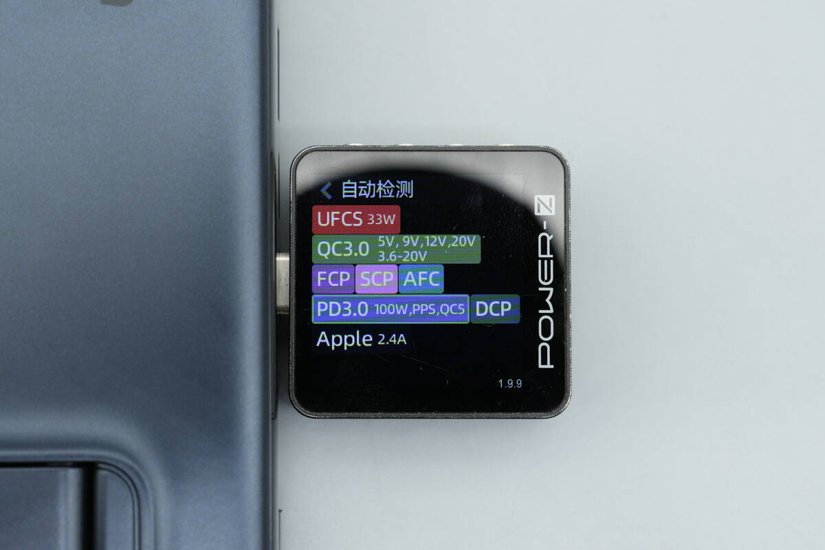
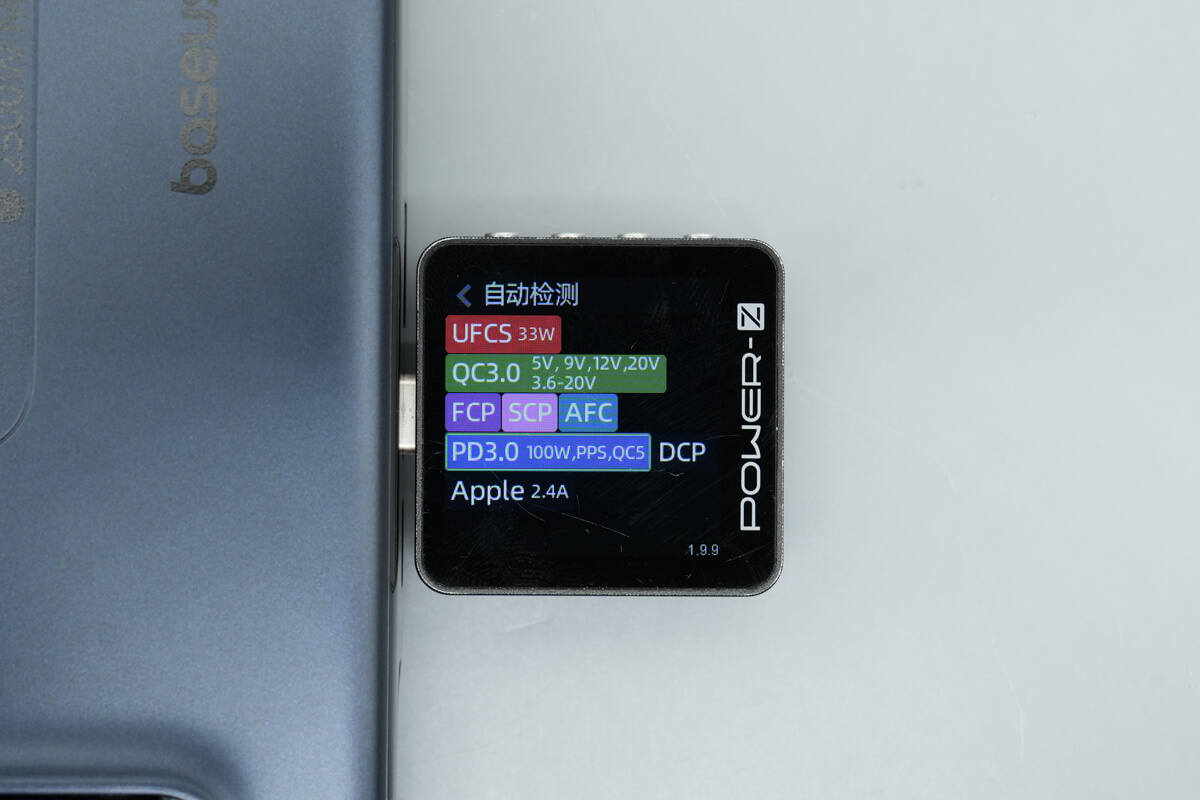
The USB-C2 ports supports QC3.0/5, FCP, SCP, AFC, PD3.0, PPS, DCP, and Apple 2.4A charging protocols.
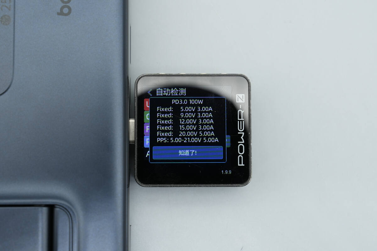
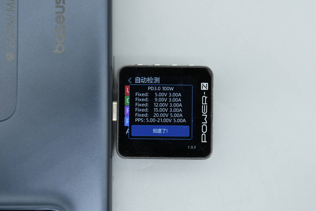
It features five fixed PDOs of 5V3A, 9V3A, 12V3A, 15V3A, and20V5A. It also has one set of PPS, which is 5-21V 5A.
The USB-C1 and USB-C2 ports support exactly the same protocols.
The PDO reports are also identical.
The USB-A port supports QC3.0, FCP, SCP, AFC, and DCP charging protocols.
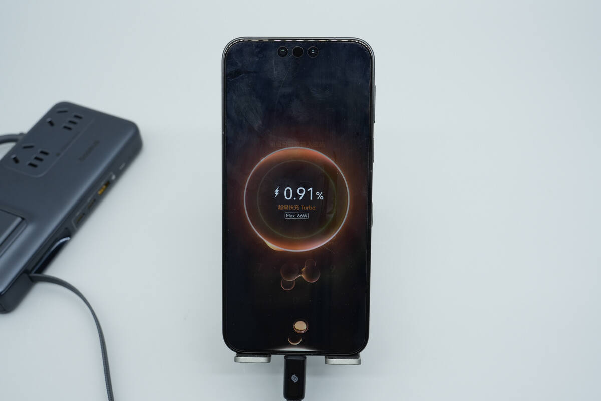
When connected to the Huawei Mate 80, it successfully initiates 66W SCP fast charging.
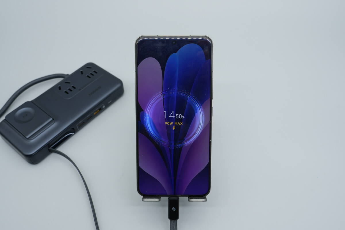
When connected to the Xiaomi 15 Pro, it successfully initiates 90W fast charging.
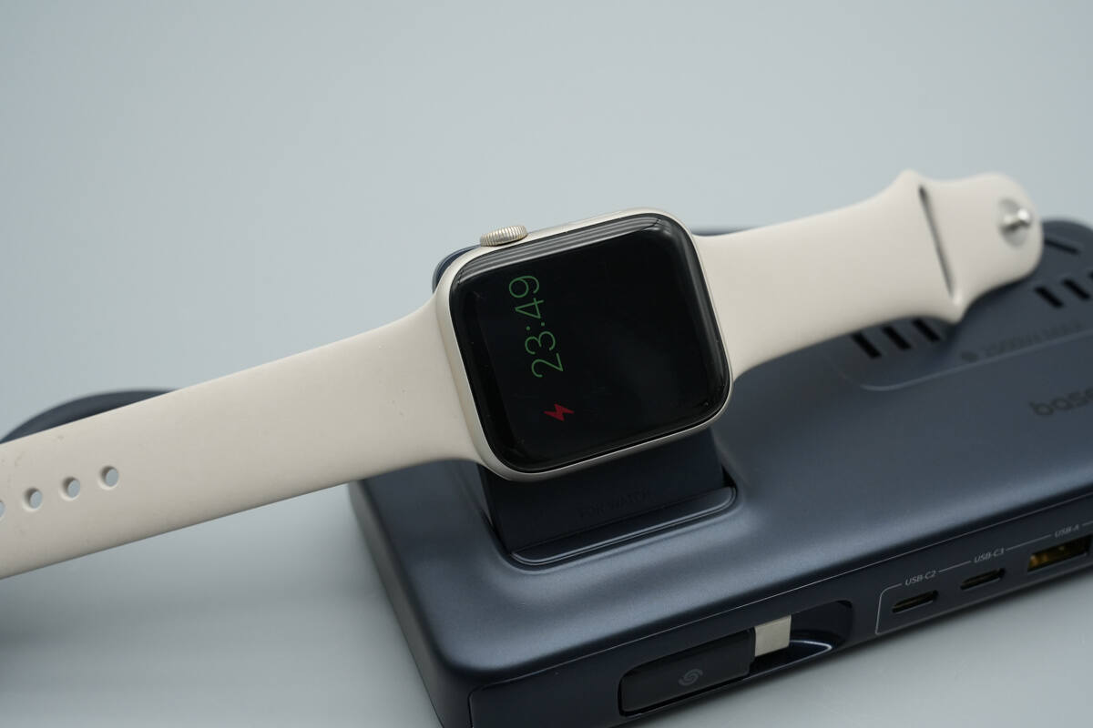
It can also wirelessly charge the Apple Watch SE.
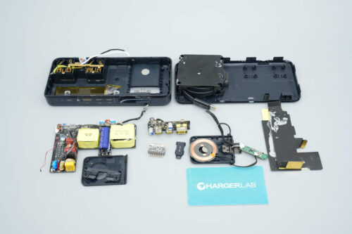
Teardown
Next, let's take it apart to see its internal components and structure.
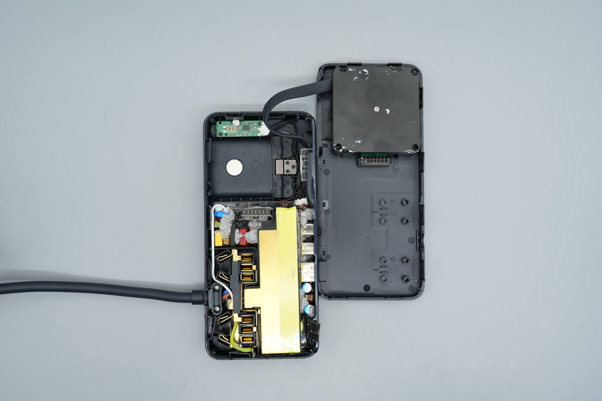
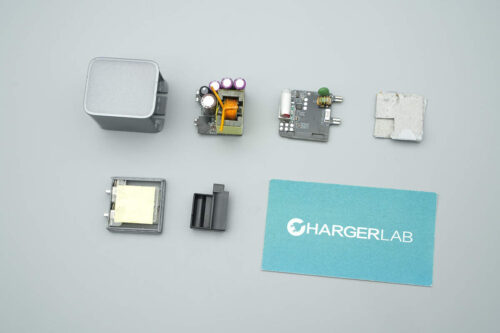
Open the case along the seam.
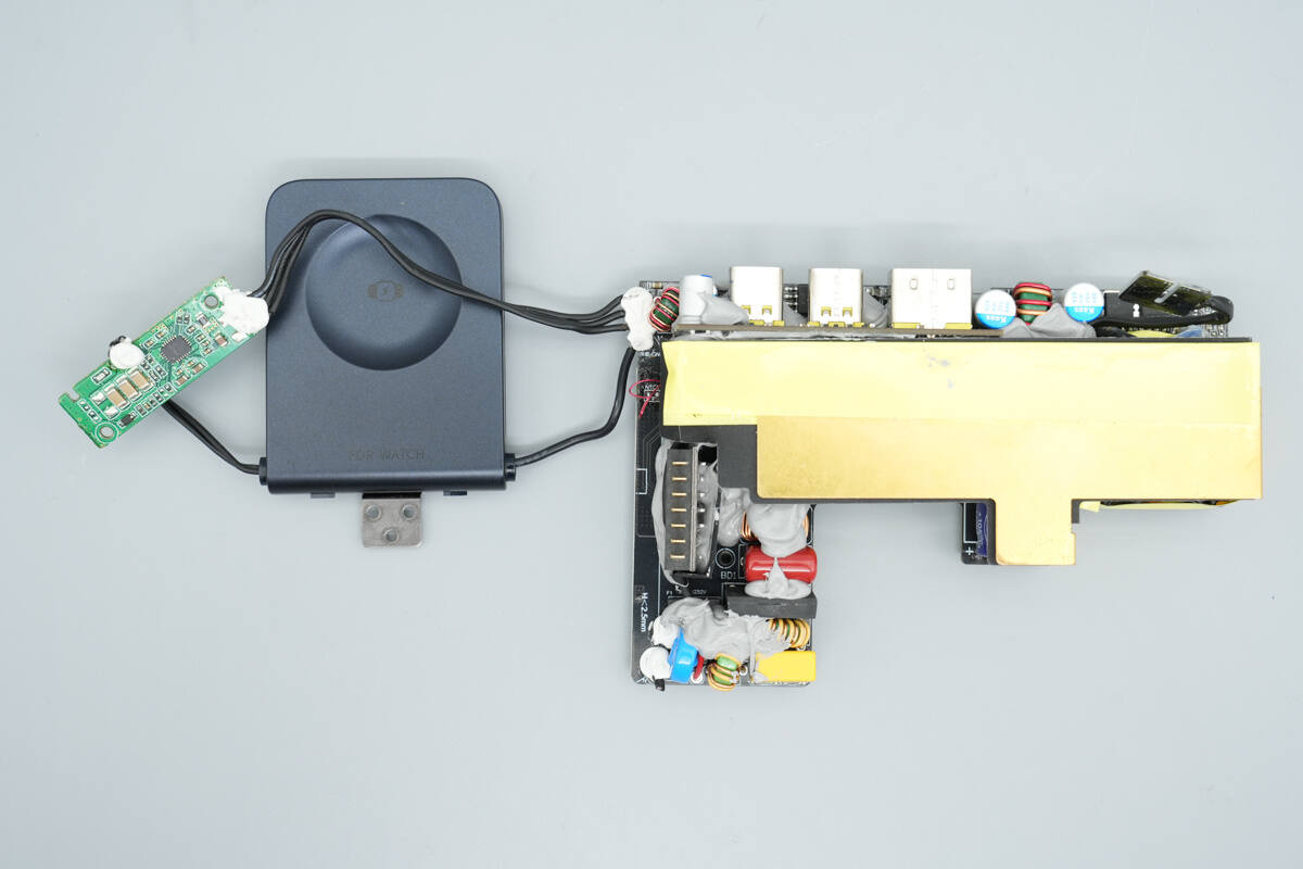
Inside, there is a socket module and a PCBA module, with the retractable cable module on the right, and the wireless charging PCBA module positioned further to the right.
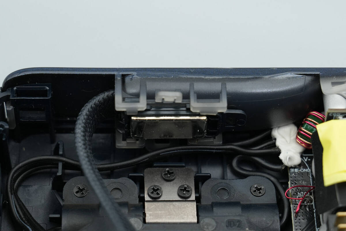
The retractable cable connector is secured in place using magnetic attachment.
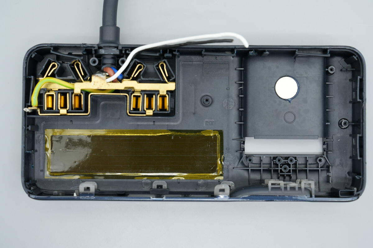
The socket module is insulated by a plastic housing, and the PCBA module is equipped with a heat-dissipating copper plate.
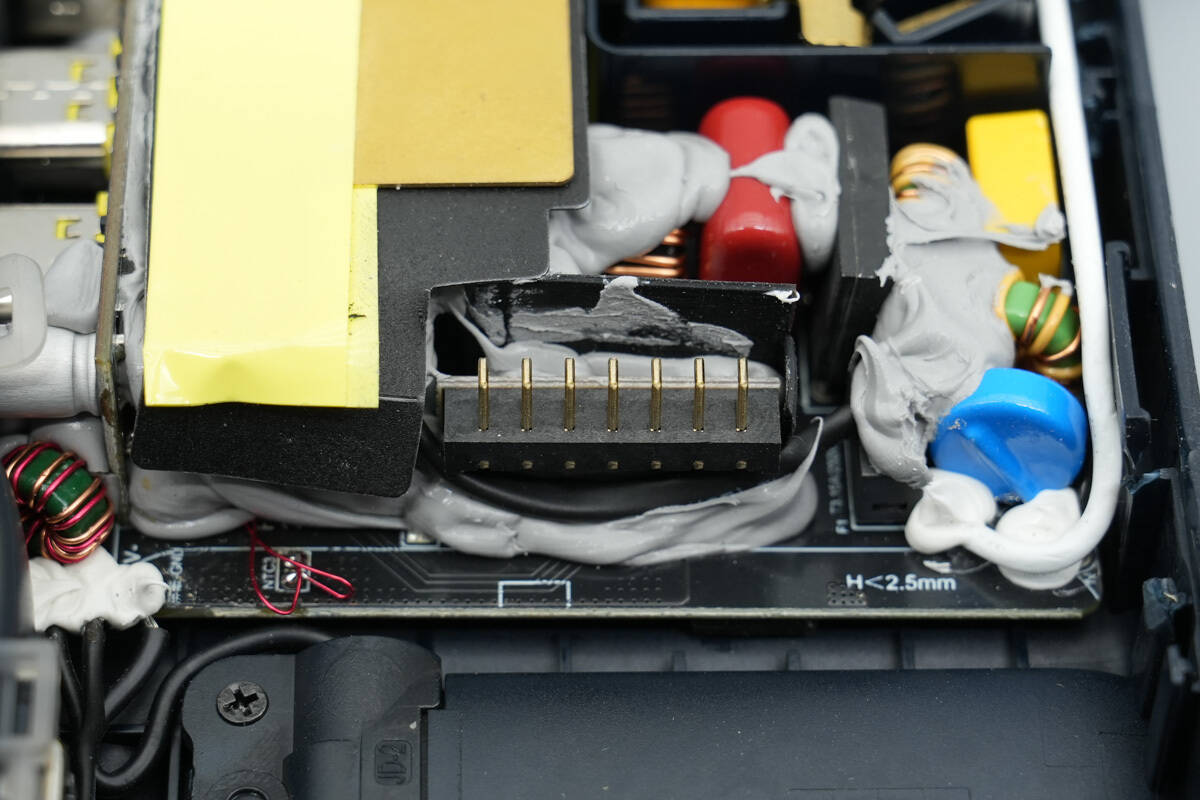
The retractable cable module is connected to the PCBA module via a connector.

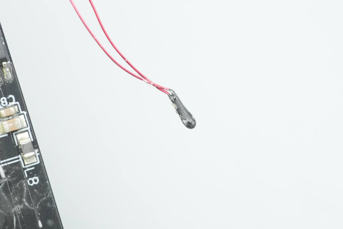
The PCBA module is connected via wires that are soldered in place, with the solder joints reinforced using adhesive.
The connecting wires were cut to remove the PCBA module. A graphite thermal pad is applied at the corresponding position of the PCBA module.
The graphite thermal pad is insulated with high-temperature adhesive tape.
The PCBA module is soldered to connect the wireless charging module.
The solder joints are reinforced with adhesive.
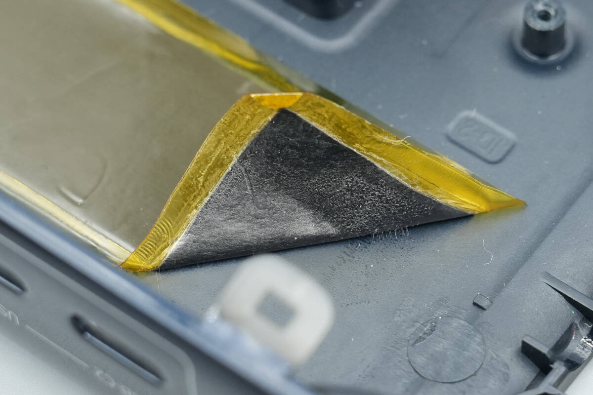
The front of the PCBA module features a brass heat sink, and internally it is insulated with a Mylar sheet.
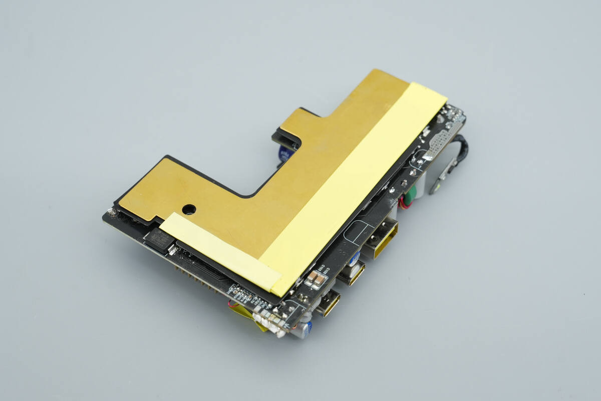
The back of the PCBA module is also equipped with a brass heat sink.
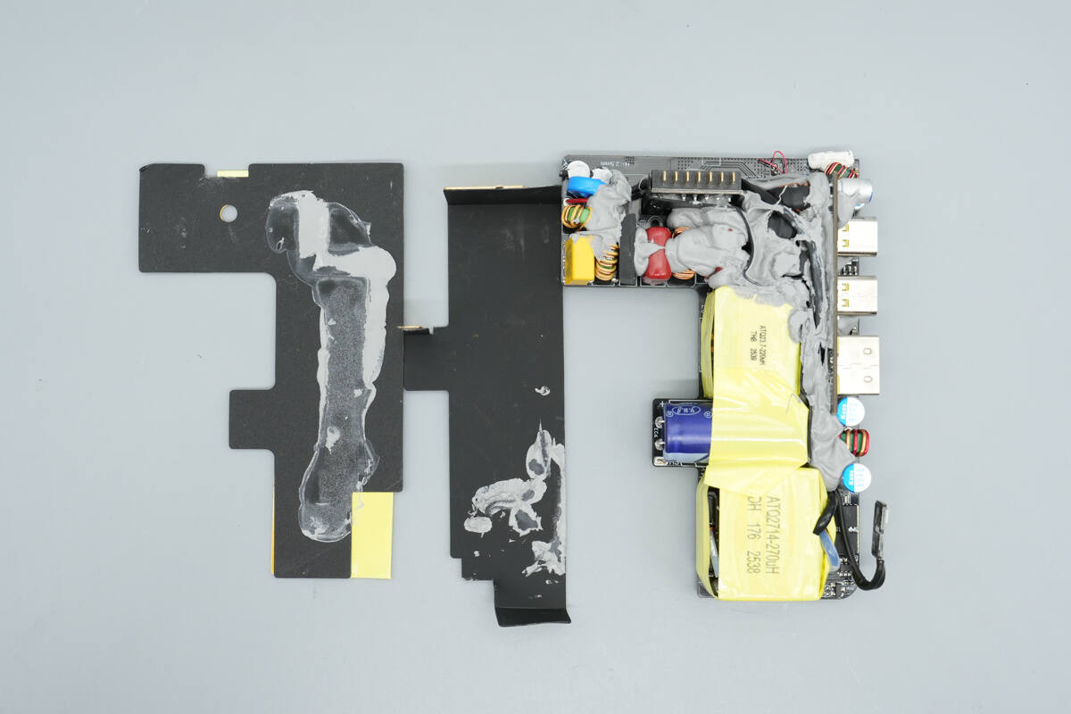
Remove the front and back heat sinks. Thermal adhesive is applied between the transformer and the inductor, and a Mylar sheet provides insulation between the high-voltage and low-voltage sides.
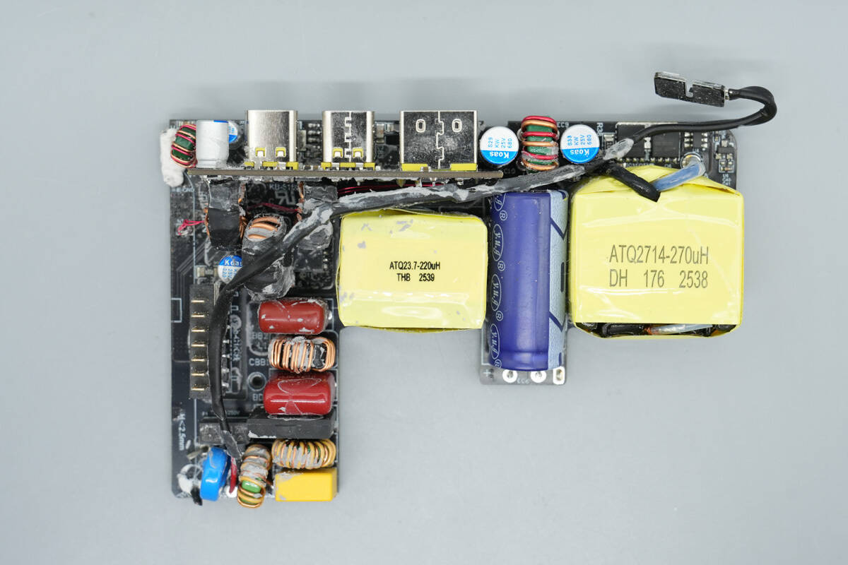
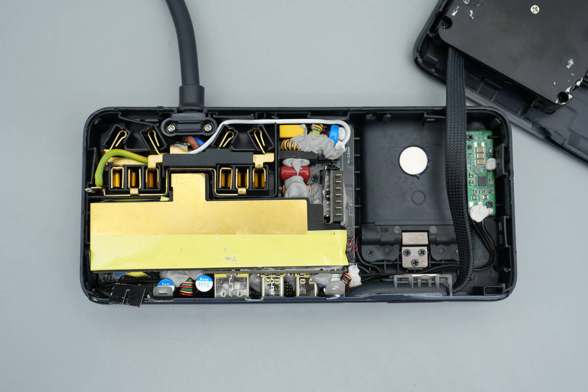
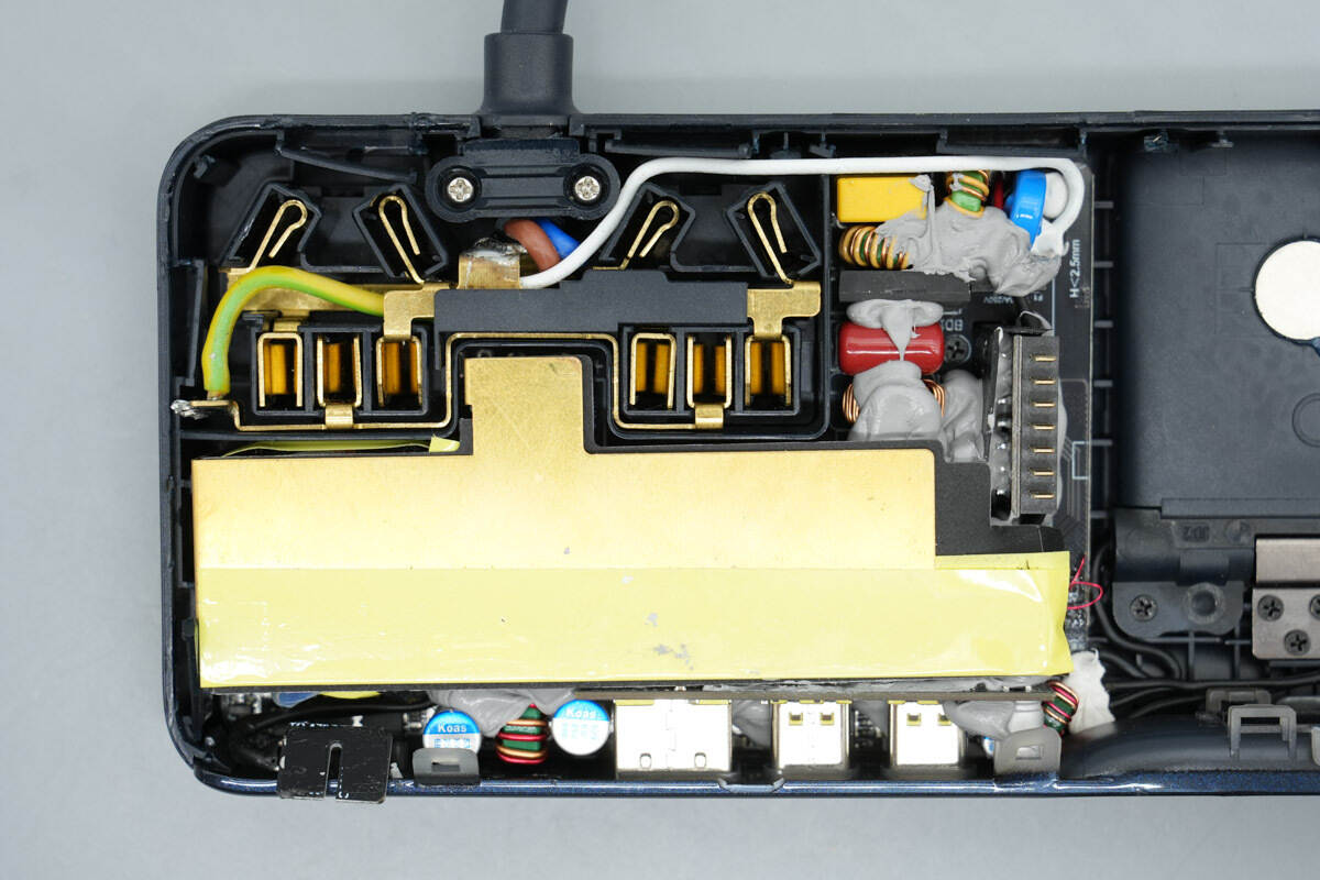
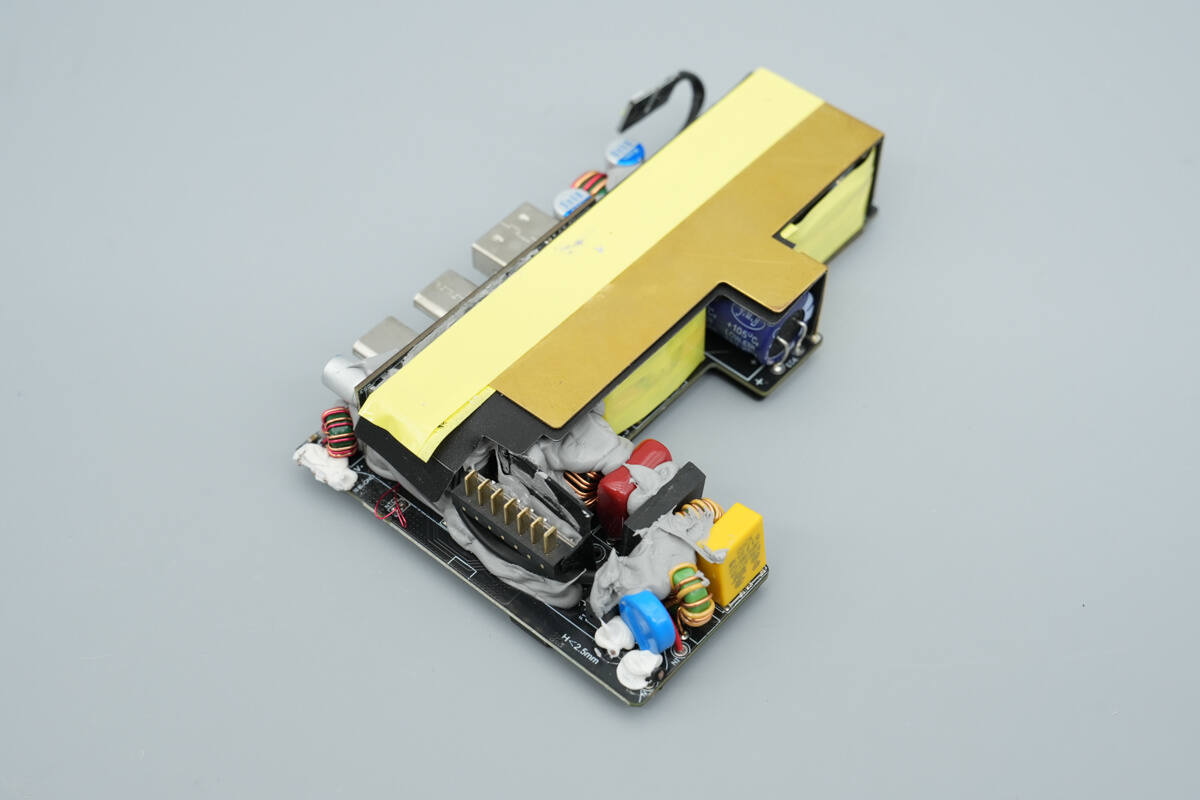
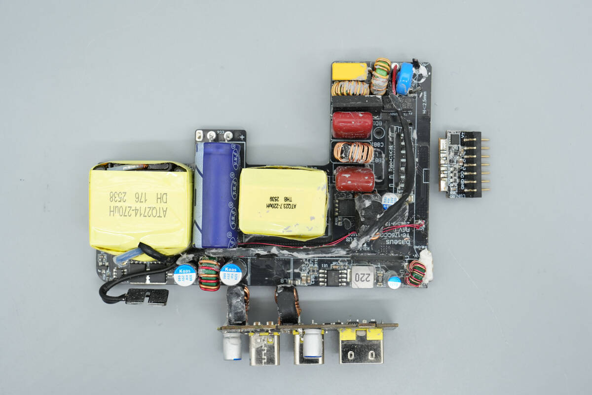
Overview of the front of the PCBA module: the lower-left corner houses the AC input terminals, including a fuse, varistor, common mode choke, safety X2 capacitor, bridge rectifier, film capacitors, and a filter inductor. Above these are the USB-C and USB-A sockets along with the buck PCB, while a buck inductor is located below.
In the central area, there is a PFC boost inductor. On the right side, high-voltage filter capacitors and the transformer are positioned. Above the transformer are the synchronous rectifier controller, synchronous rectifiers, and solid capacitors.
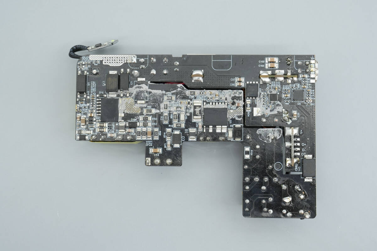
On the back, there are SMD Y capacitors, a GaN PFC chip and a GaN flyback chip, a feedback optocoupler, protocol chips, a synchronous buck controller, and synchronous buck MOSFETs. A slot is cut between the primary and secondary sides, with a Mylar sheet inserted for insulation.
The buck PCB and output socket PCB were removed to continue the disassembly.
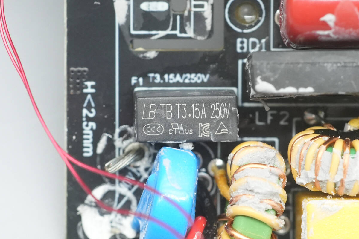
The fuse at the input comes from Lanbao, with a specification of 3.15A 250V.
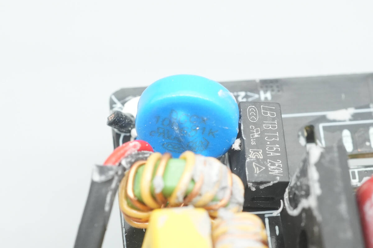
The varistor is from DGCX, model 10D681K, and is used to absorb overvoltage surges.
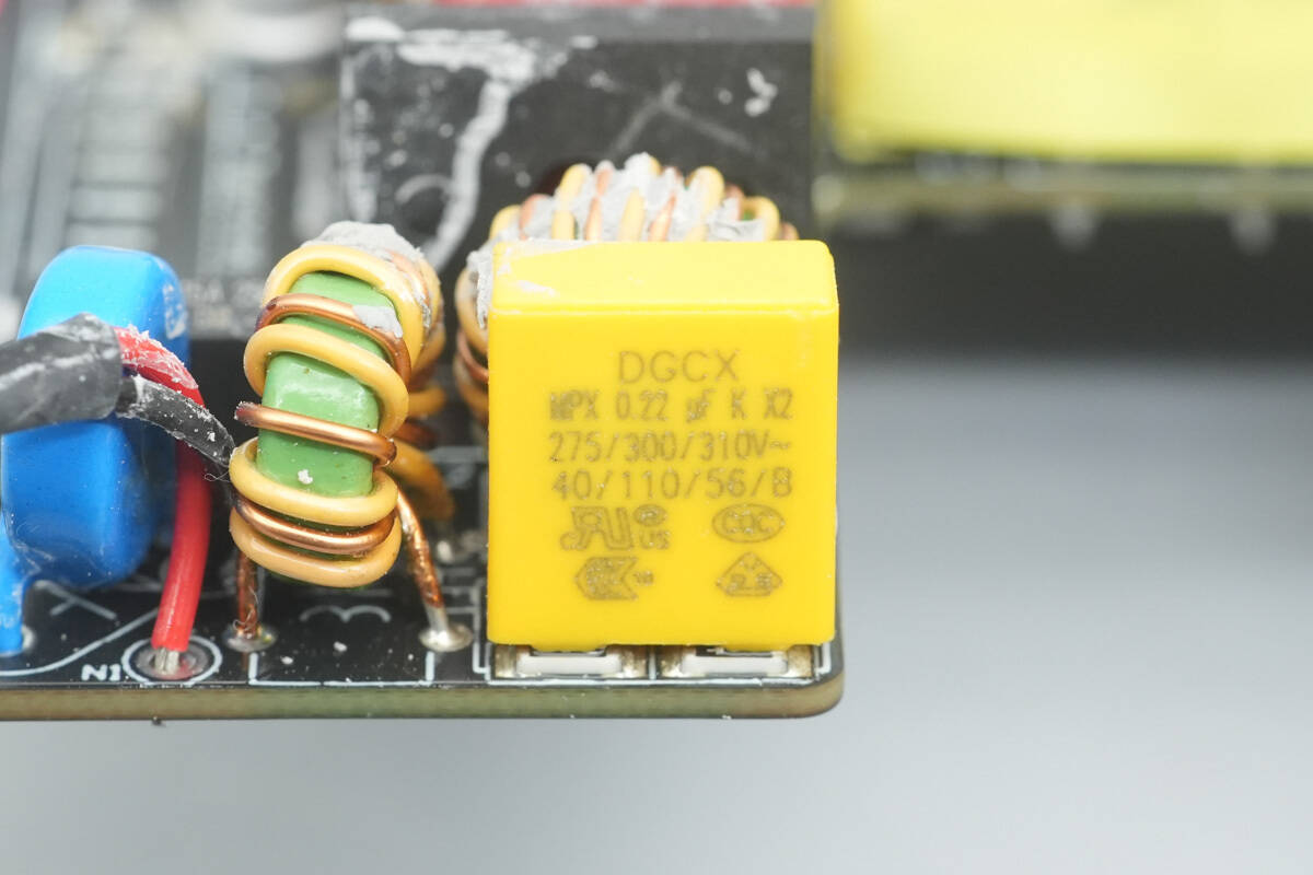
The safety X2 capacitor is from DGCX, with a capacitance of 0.22μF, and features a discharge resistor at the bottom.
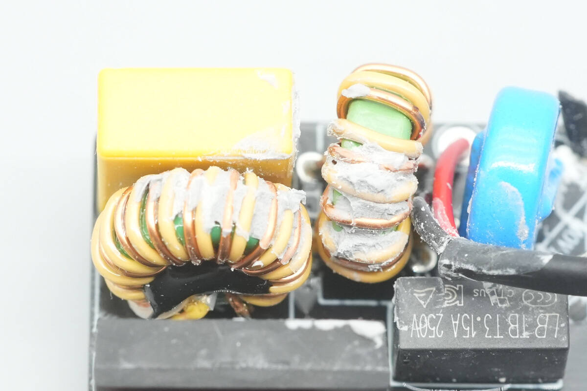
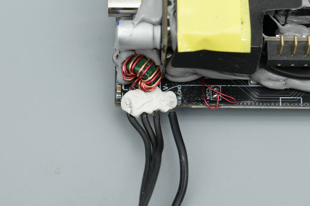
The common mode choke is wound using enameled wire and insulated wire.
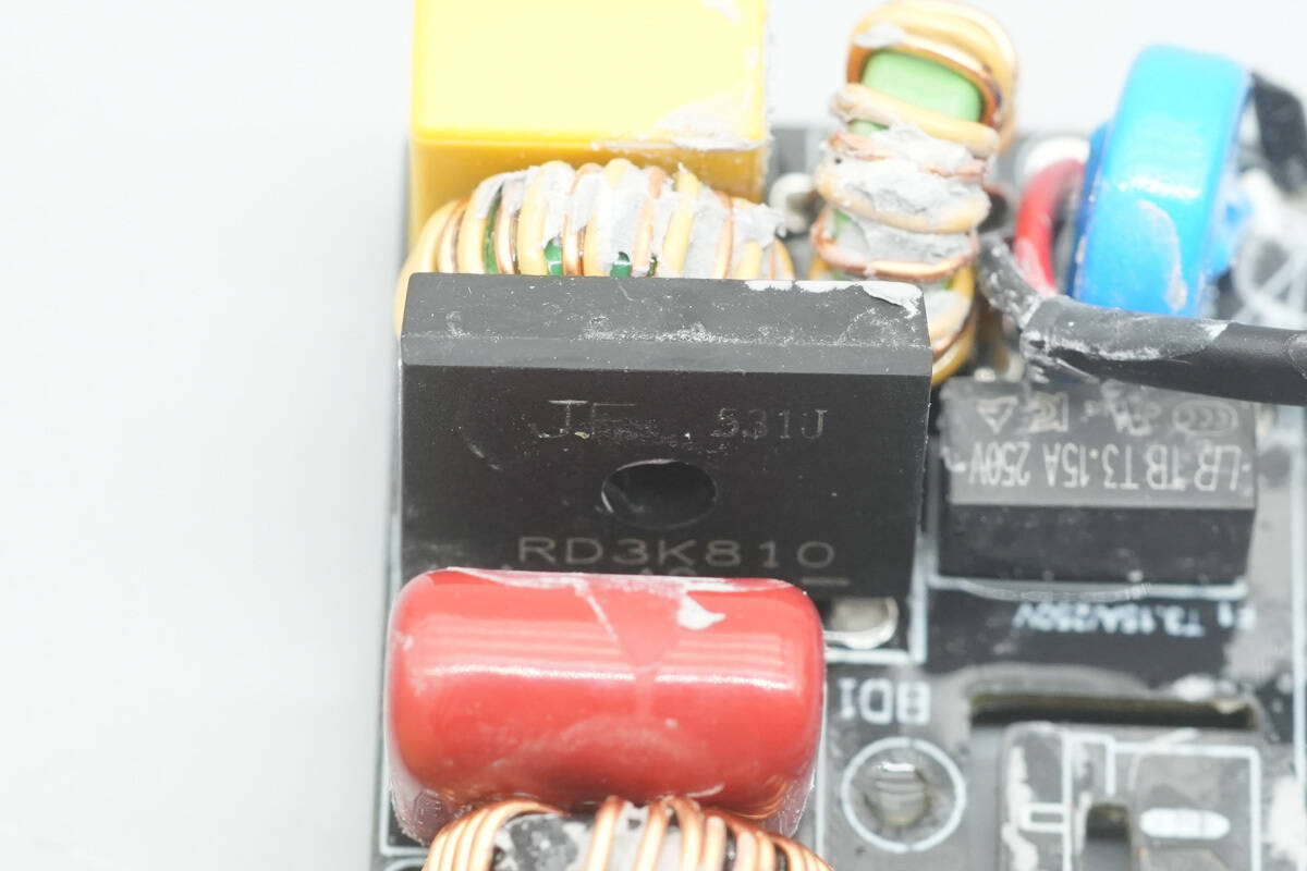
The bridge rectifier is from JF, model RD3K810, rated at 1000V 8A, and uses a D3K package.
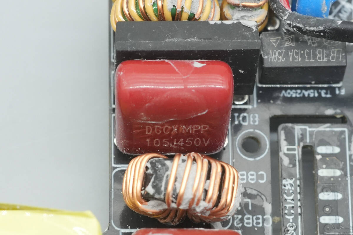
The film capacitor is from DGCX, with a specification of 1μF 450V.
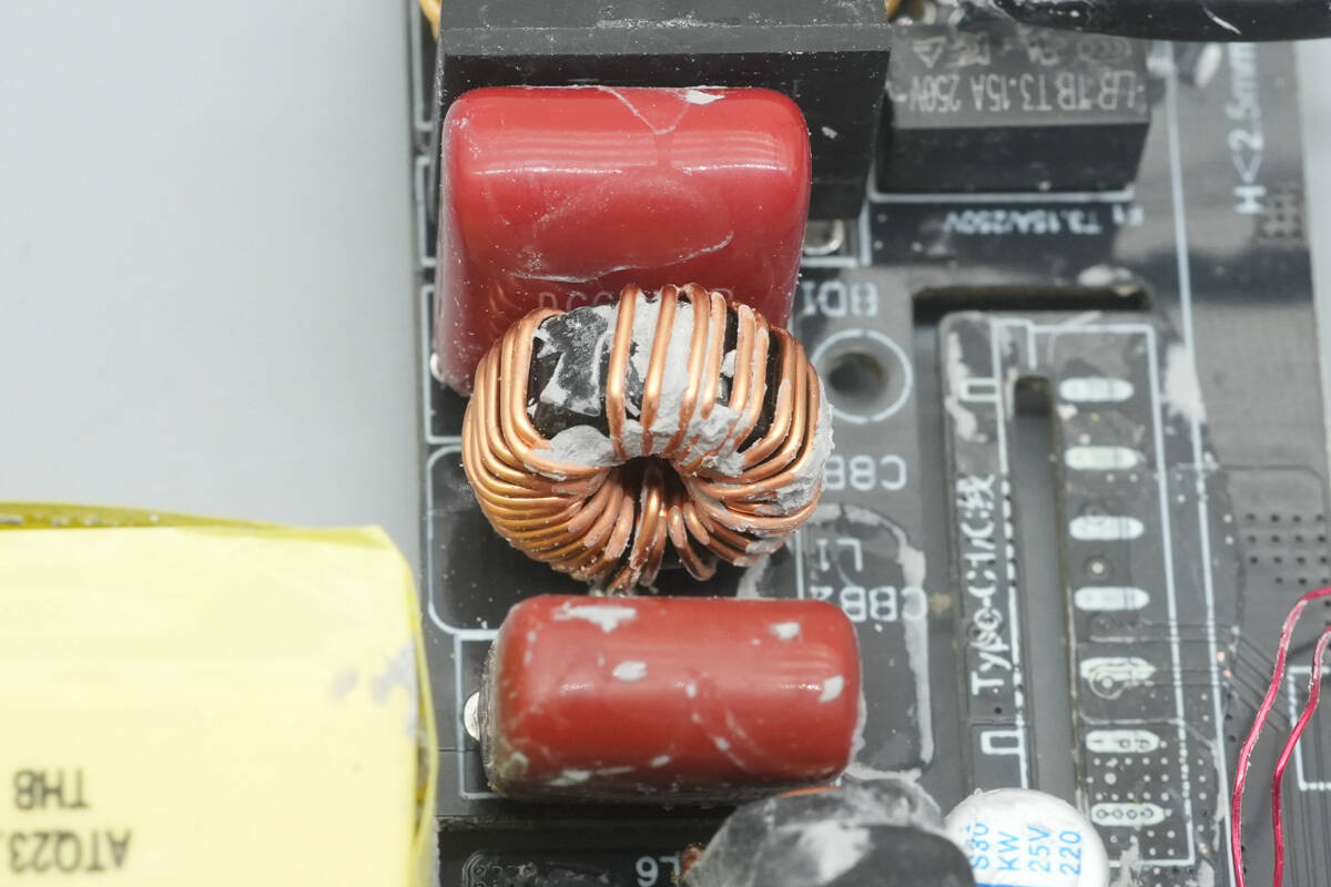
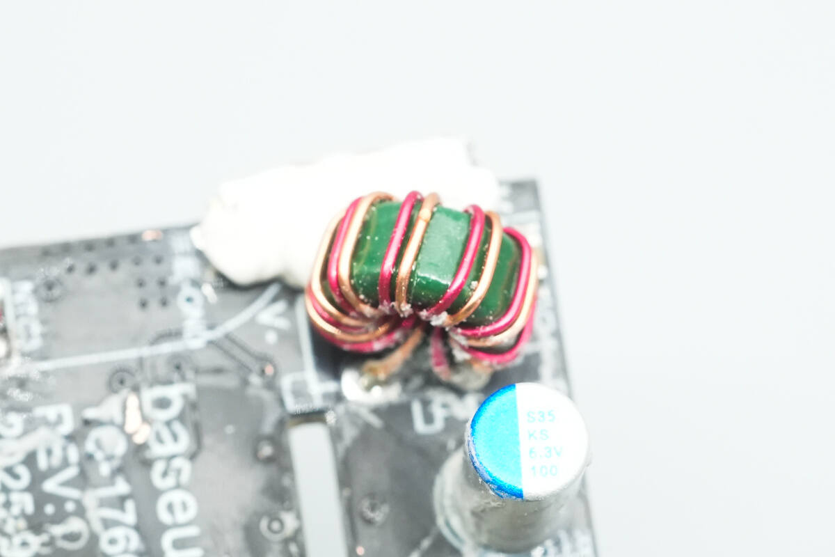
The filter inductor is wound using a magnetic core.
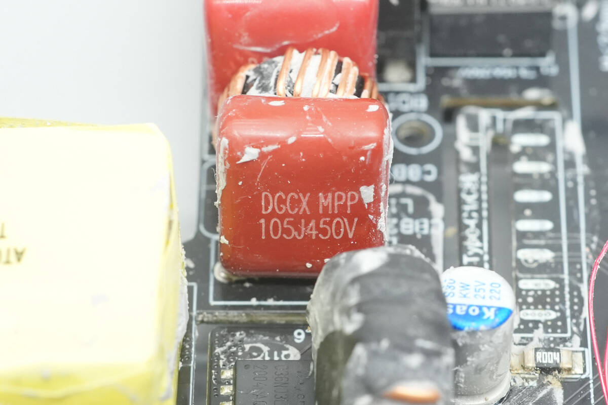
Another film capacitor with the same specification is also used.
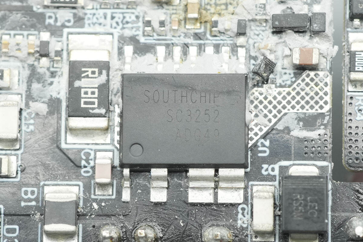
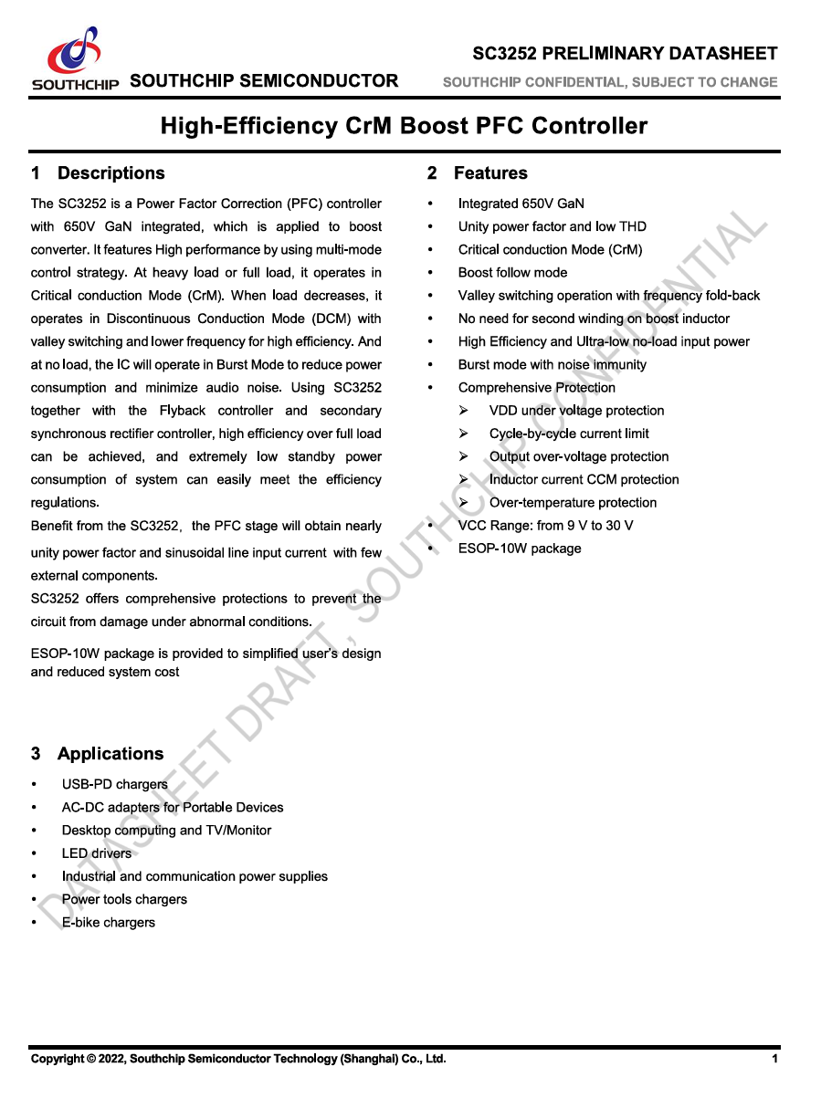
The PFC GaN IC is from SouthChip, model SC3252. It is a PFC controller that integrates a 650V GaN FET. The chip supports multiple control modes: operating in critical conduction mode (CCM) under heavy and full loads, and in discontinuous conduction mode (DCM) under light loads. It achieves high efficiency through valley switching and reduced switching frequency. The chip supports boost follower mode without requiring an auxiliary winding.
The SC3252 also supports burst mode operation for high conversion efficiency across the full load range. It provides undervoltage protection, cycle-by-cycle overcurrent protection, output overvoltage protection, continuous inductor mode protection, and overtemperature protection. It operates with a supply voltage of 9–30V and comes in an ESOP-10W package.
Here is the information about SouthChip SC3252
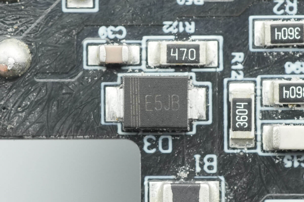
The PFC rectifier is model E5JB, an ultra-fast recovery diode rated at 600V 5A, and uses an SMBF package.
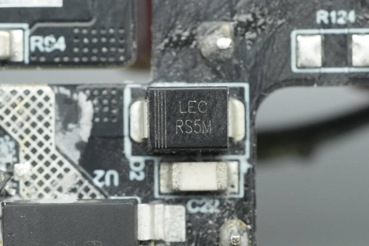
The bypass diode is from LEC, model RS5MB, a fast recovery diode rated at 1000V 5A, and uses an SMB package.
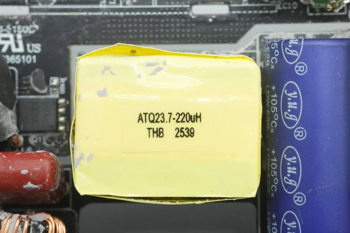
The PFC boost inductor is wound on an ATQ23.7 magnetic core, with an inductance of 220 μH, and is tightly insulated with adhesive tape.
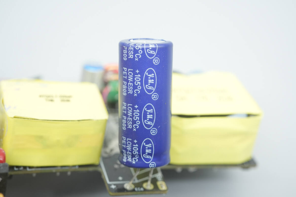
The high-voltage filter capacitor is from y.u.g.
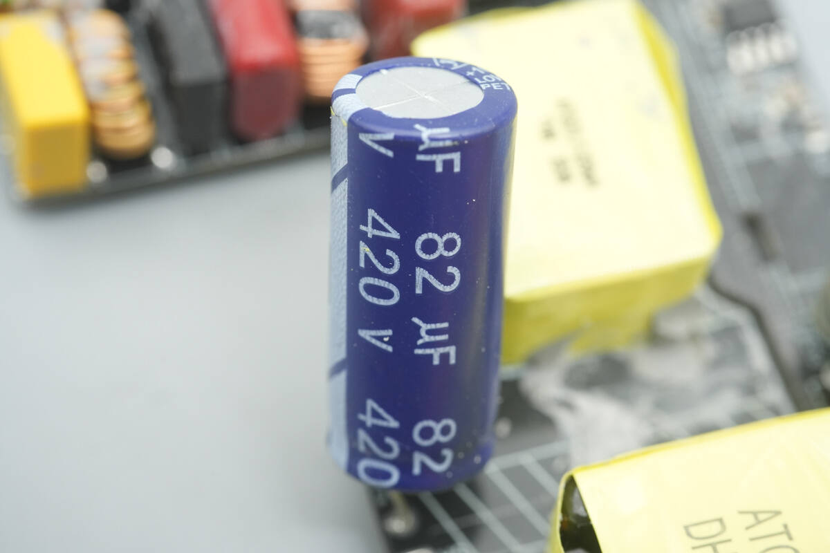
It has a specification of 82 μF, 400 V.
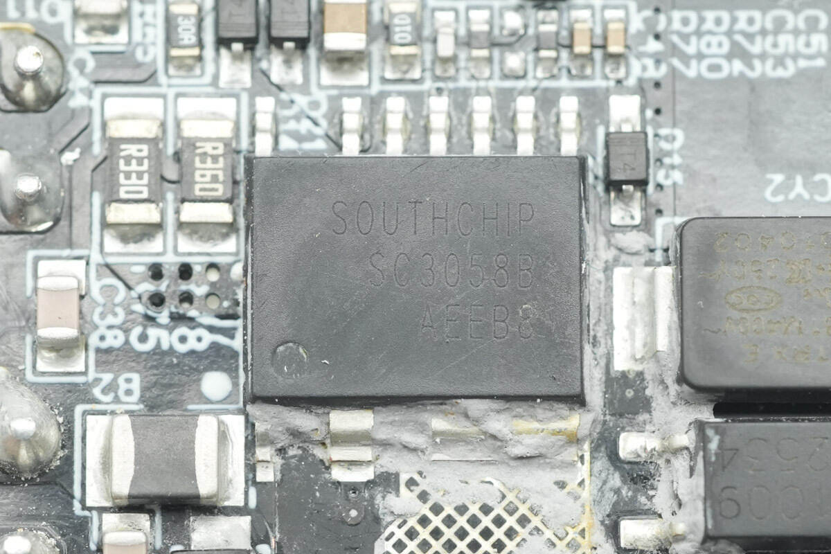
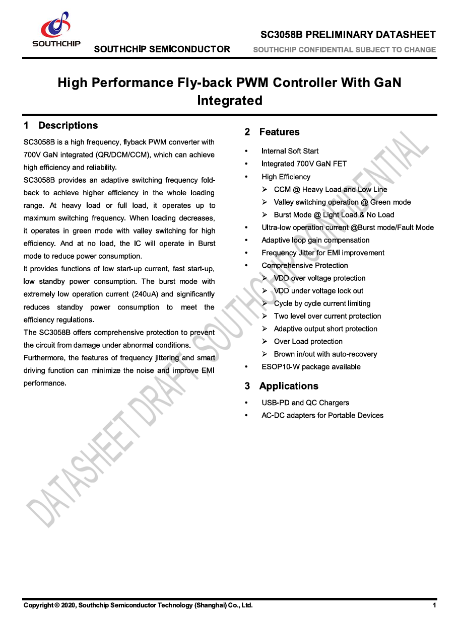
The GaN IC is from SouthChip, model SC3058B. The chip integrates a high-performance multi-mode flyback controller and a 700V GaN FET. It supports adaptive frequency folding, providing high conversion efficiency across the full load range. The chip features extremely low standby current and supports adaptive loop gain compensation.
The SC3058B includes overvoltage and undervoltage lockout protection, cycle-by-cycle overcurrent protection, two-stage overcurrent protection, adaptive output short-circuit protection, and overload protection. It is suitable for USB-PD fast charging and power adapter applications, and comes in an ESOP-10W package.
Here is information about SouthChip SC3058B.
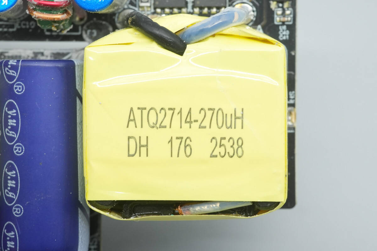
The transformer uses an ATQ2714 magnetic core and is tightly insulated with adhesive tape.
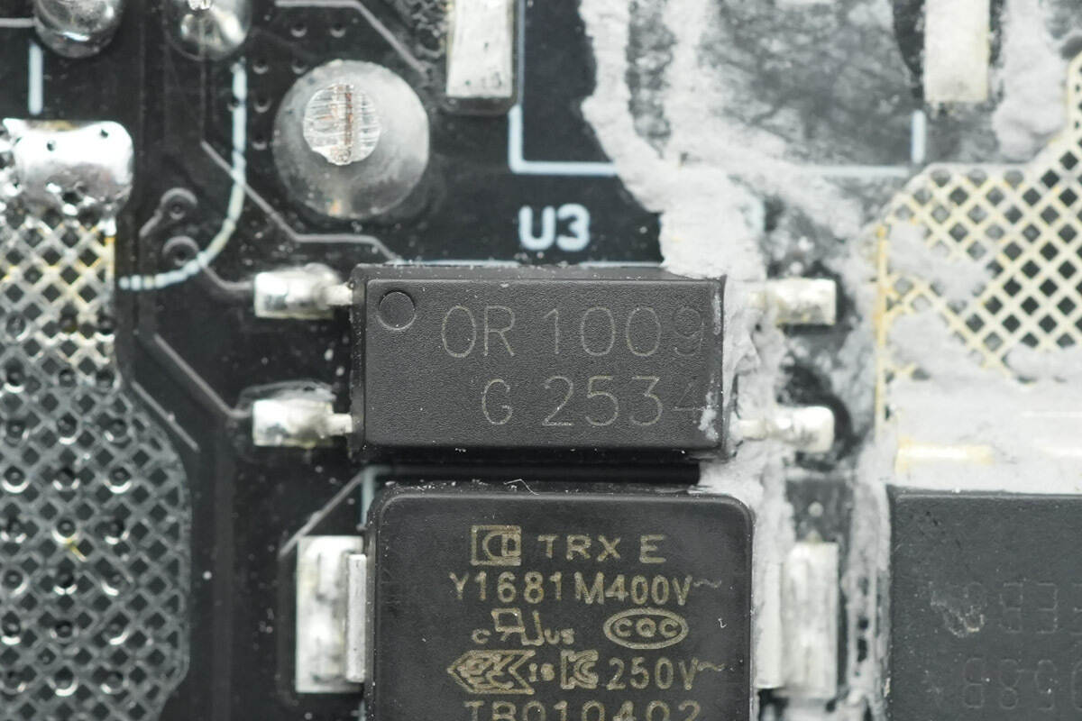
The optocoupler is from OR, model OR1009.
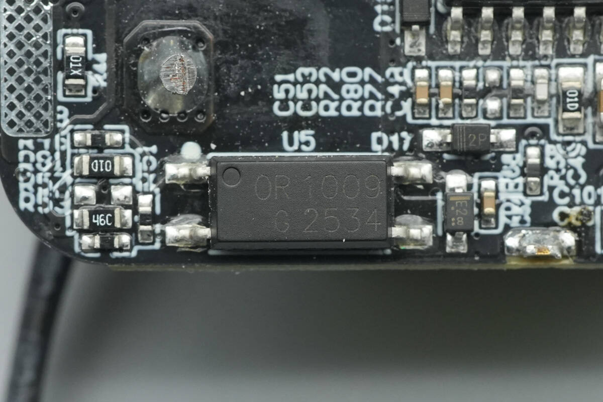
Another optocoupler of the same model is also used.
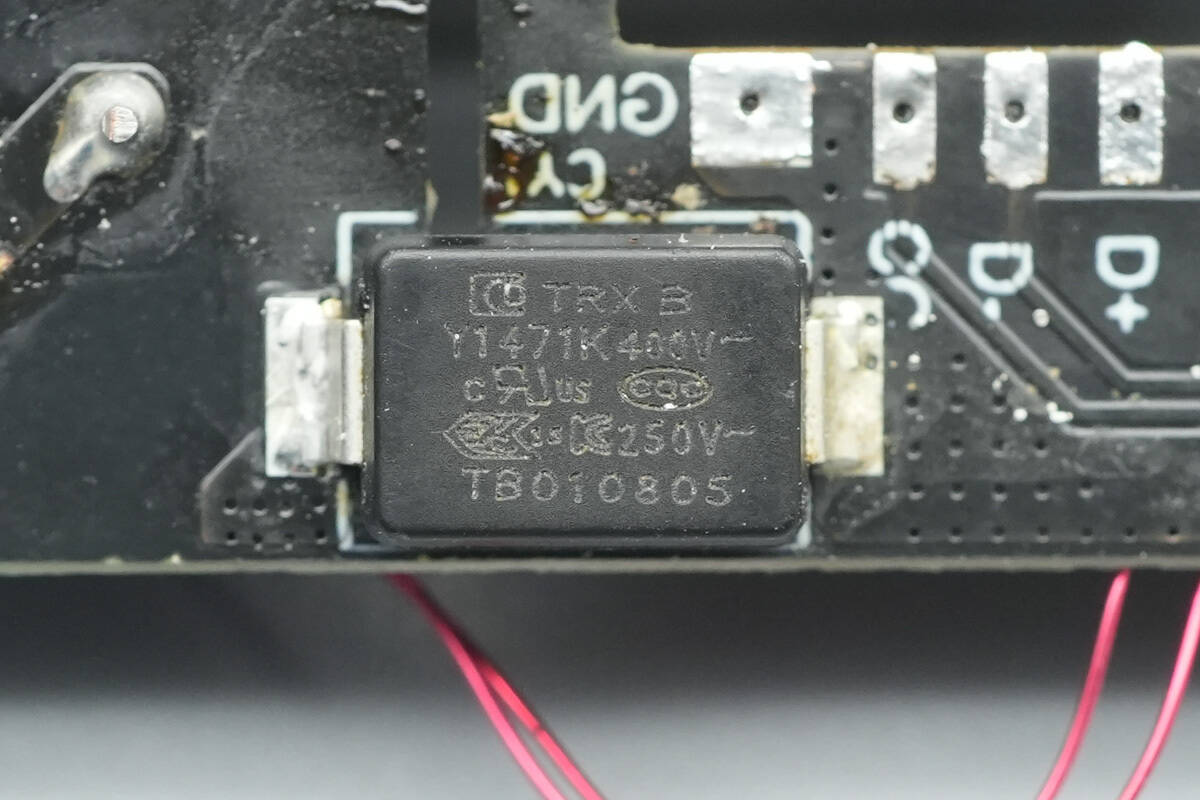
The SMD Y capacitors are from TRX. Their compact size and light weight make them well-suited for high-density power products such as GaN fast chargers. The part numbers are TMY1471K and TMY1681K.
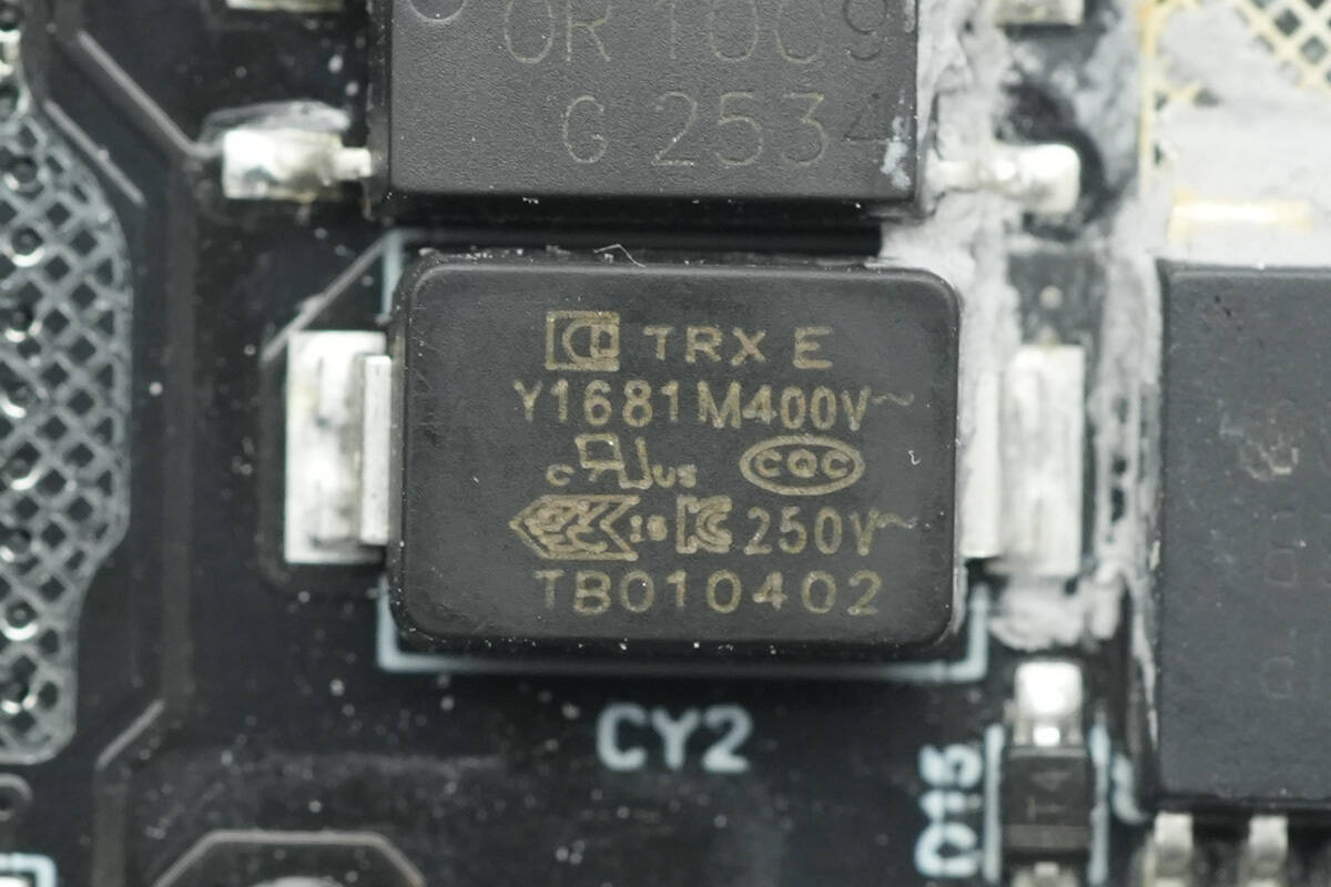
Close-up of another TRX SMD Y capacitor.
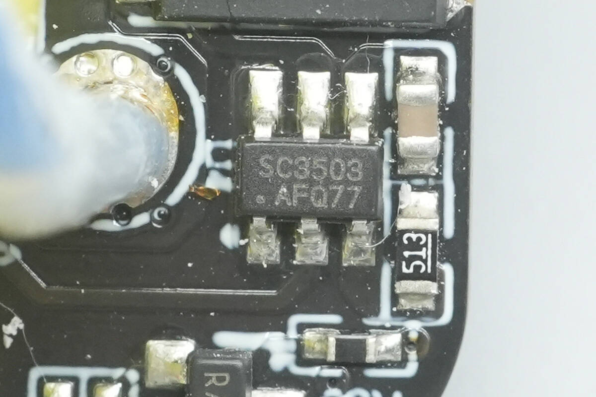
The synchronous rectifier controller is a SouthChip SC3503. It is an adaptive turn-on detection and fast turn-off synchronous rectifier controller that does not require an auxiliary winding for power. The output voltage can go as low as 0 V. Its patented adaptive turn-on detection circuit prevents false turn-on of the synchronous rectifier, is compatible with a wide range of MOSFETs, and features ultra-low quiescent current. It supports multiple operating modes, high-side and low-side synchronous rectification, and requires very few external components. The chip comes in an SOT23 package and is suitable for wide-range flyback adapter applications.
Here is the information about SouthChip SC3503.
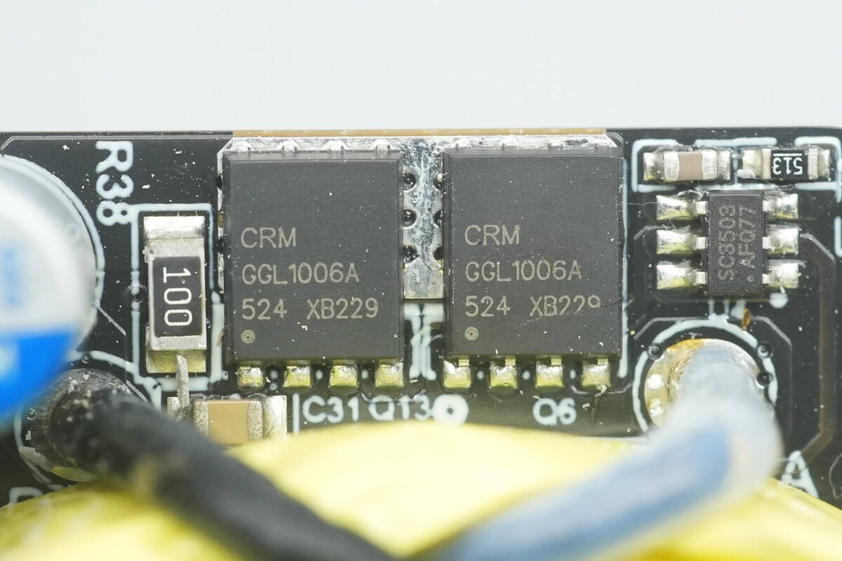
The synchronous rectifiers are from CRM, model CRMGGL1006A. They are NMOS devices with a voltage rating of 100 V and an on-resistance of 5.6 mΩ, packaged in PDFN 5×6‑8L.
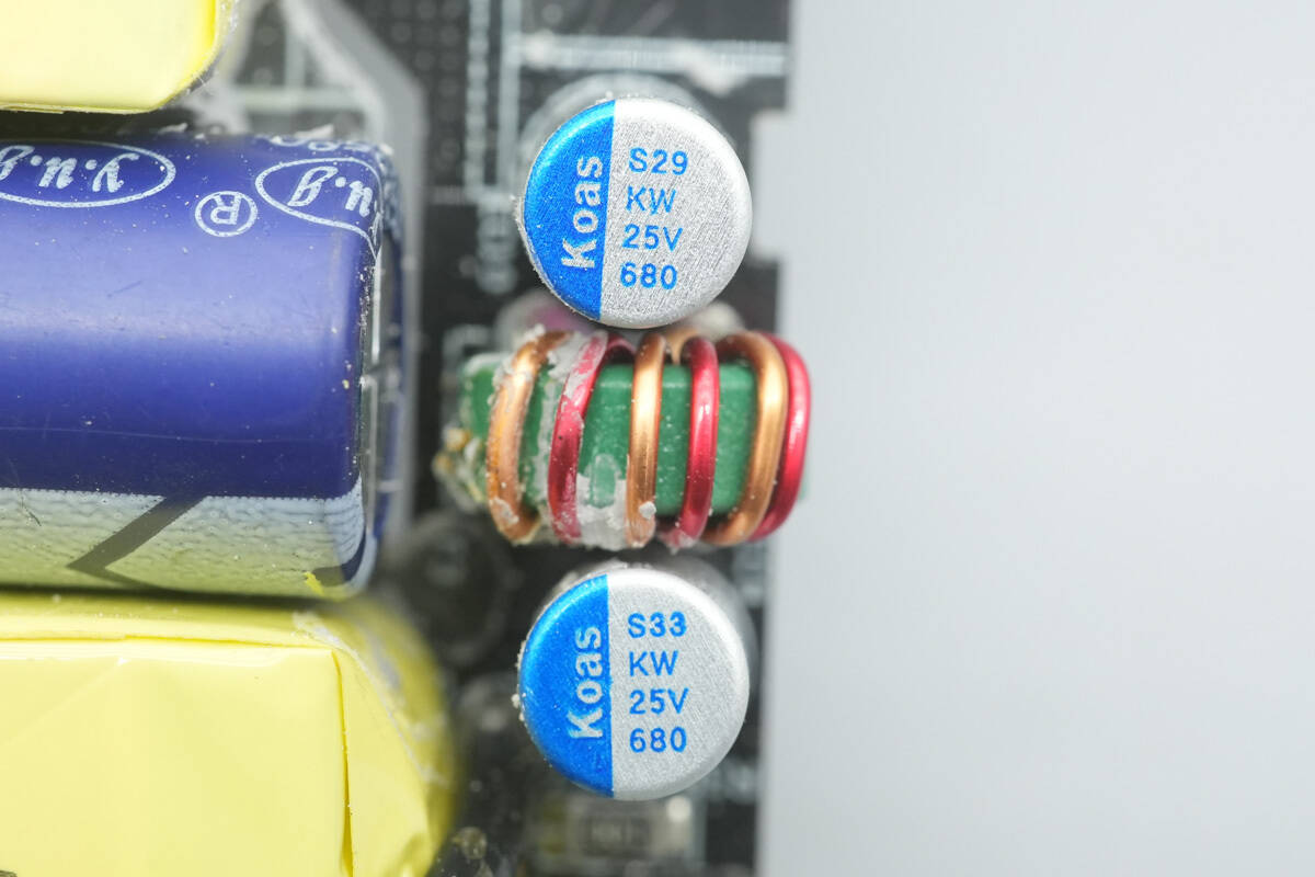
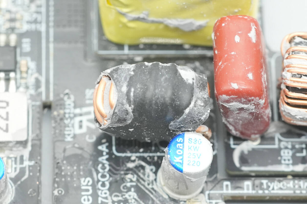
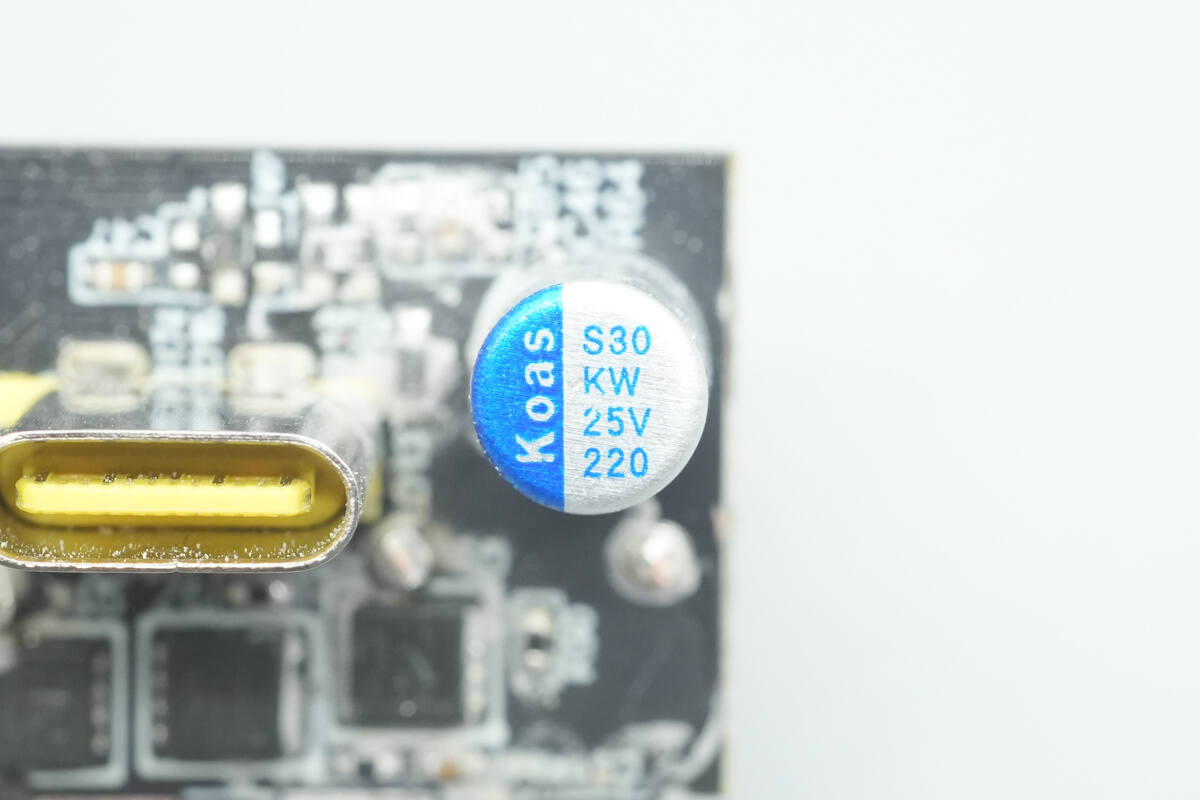
The output filter capacitor is from Koshin, part of the KW series rated for 125 ℃, with a specification of 25 V 680 μF.
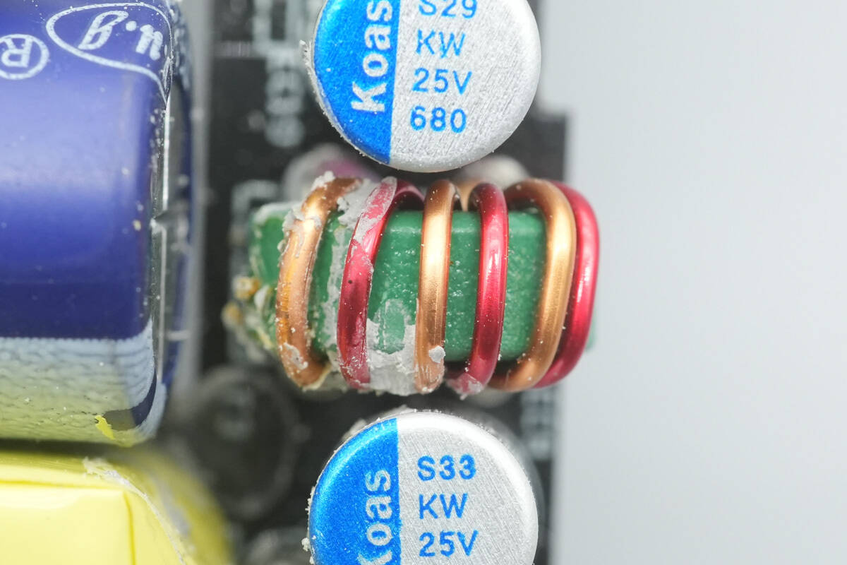
The filter inductor is wound using enameled wire.
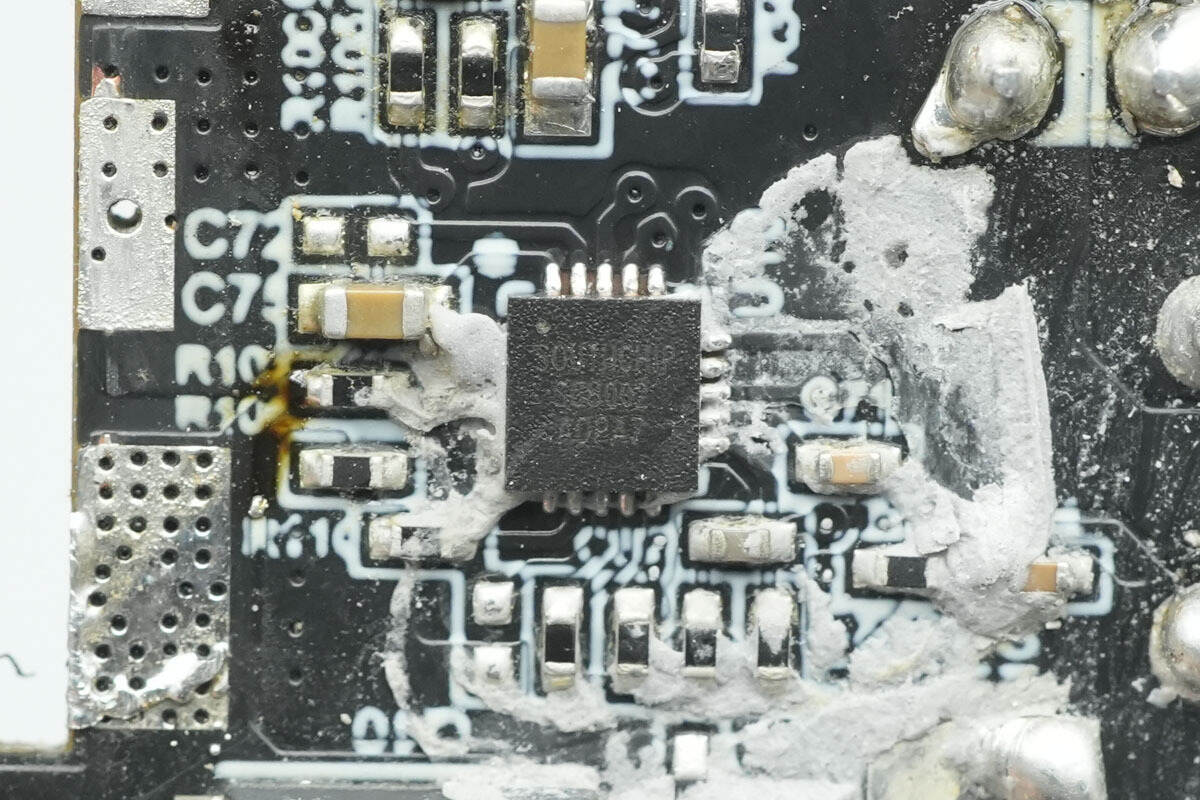
The synchronous buck controller from SouthChip, model SC8002, supports an input voltage range of 4.6–36V. The output voltage is adjustable, with support for fixed 5V output and fast-charging applications. The IC features high-precision output current limiting, dual-channel independent current limiting, and comprehensive built-in protection functions. SC8002 comes in a QFN 3×3-20 package and is suitable for car chargers, multi-port chargers, USB hubs, and other applications.
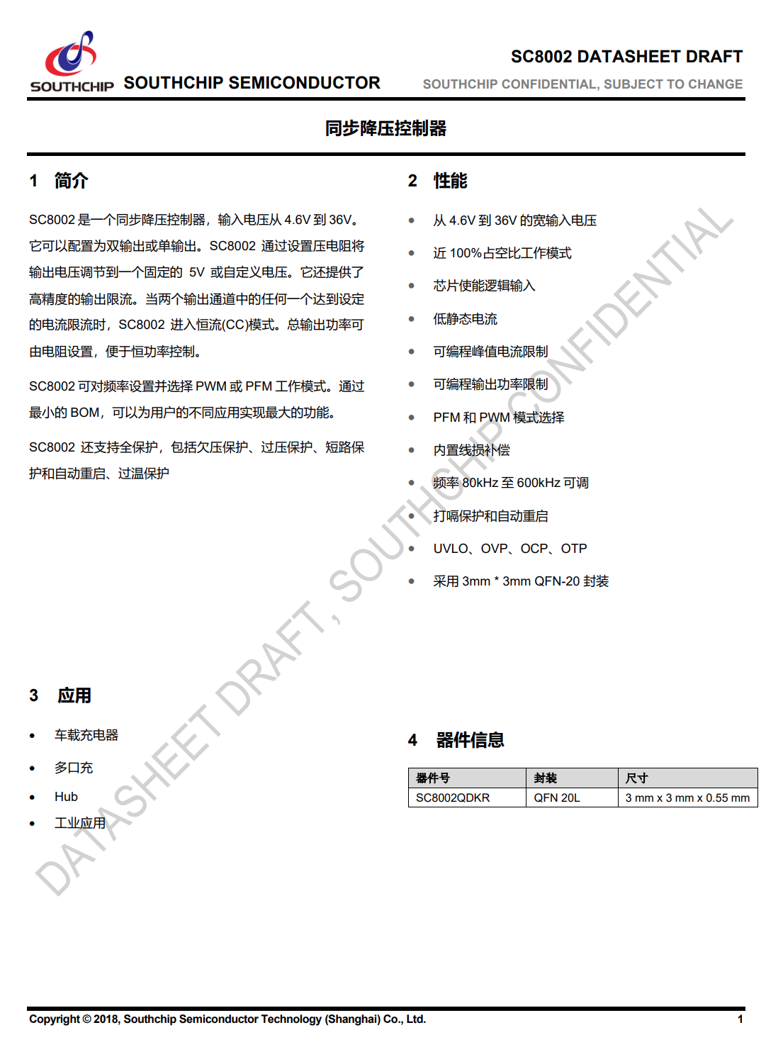
Here is the information about SouthChip SC8002.
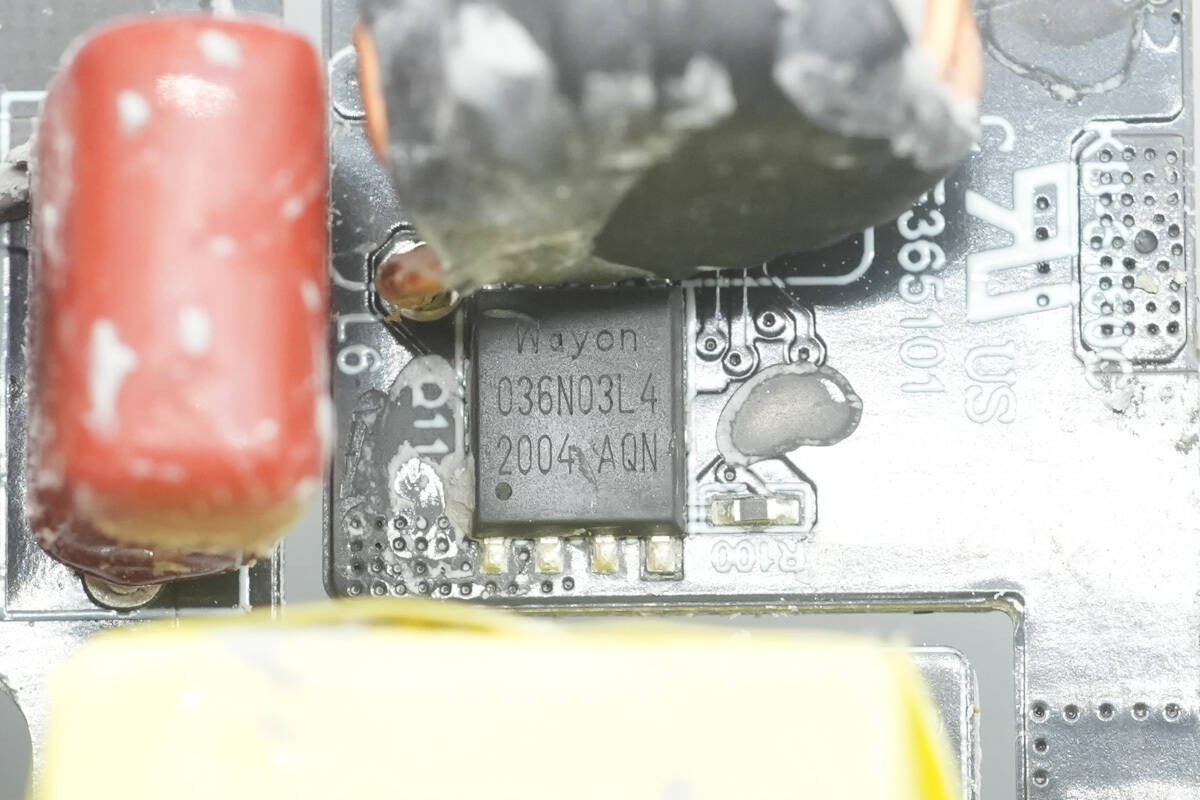
The buck MOSFET from WAYON, model WMB036N03LG4, is an NMOS with a voltage rating of 30V and an on-resistance of 2.6 mΩ. It comes in a PDFN5060-8L package.
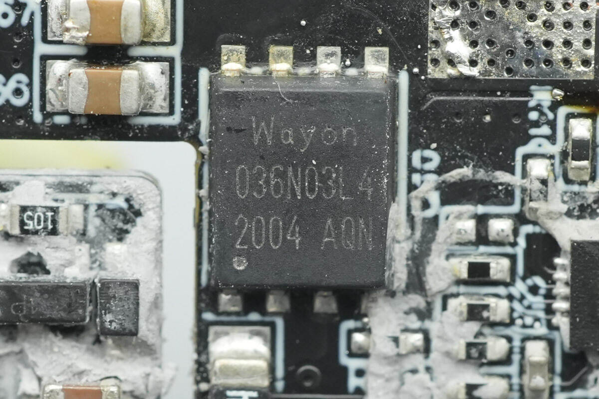
Another buck MOSFET of the same model.
The buck inductor is wound with enameled wire and insulated with a heat shrink tube.
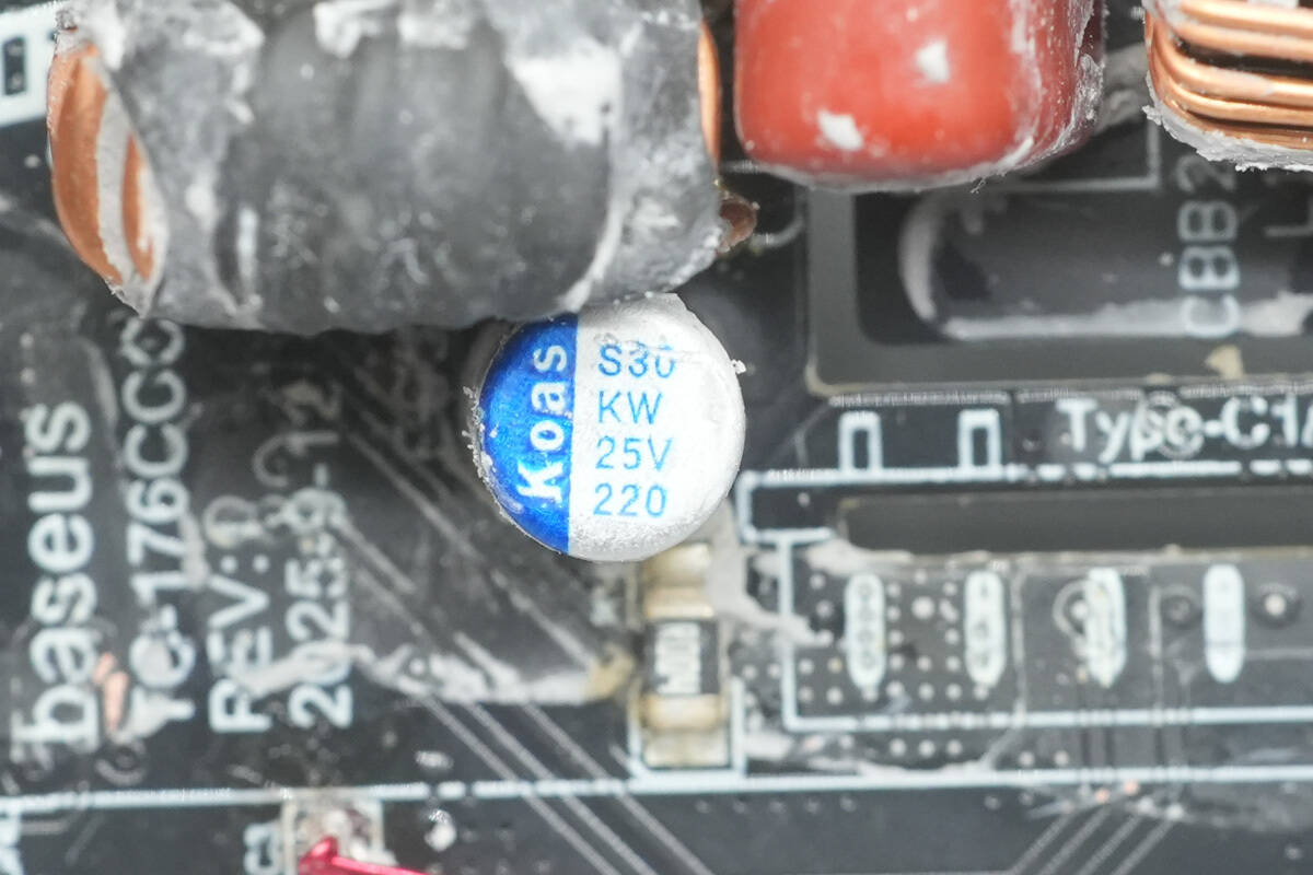
The output filter capacitor has a specification of 25V, 220μF.
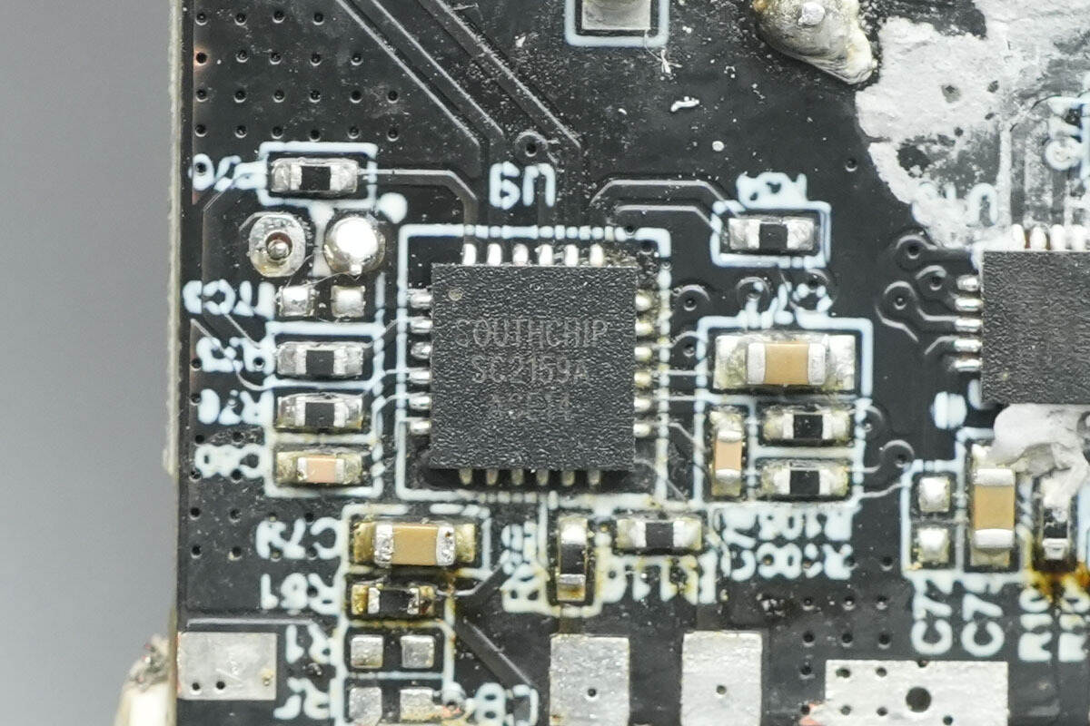
The protocol chip from SouthChip, model SC2159A, is a high-performance fast-charging controller compatible with mainstream high-voltage fast-charging protocols. It supports PD 3.2 applications through the CC pin and BC1.2, UFCS, and various proprietary protocols via the DPDM pin. This chip integrates core modules such as USBPD baseband PHY, Type-C detection, and DPDM protocol PHY, paired with a 32-bit high-performance MCU, 64KByte MTP & ROM, and 2.5KByte SRAM, providing a cost-effective solution for applications.
The chip operates with a VBUS voltage range of 3.0V to 22V (withstanding up to 28V) and features an 11-bit VDAC and a 10-bit IDAC. It also supports transformer node voltage detection and power IC control interfaces like I²C/OPTO. Additionally, the chip includes comprehensive protection mechanisms, such as over-voltage, under-voltage, and over-current protections. With a QFN24 package, it ensures stable and reliable operation in diverse fast-charging scenarios.
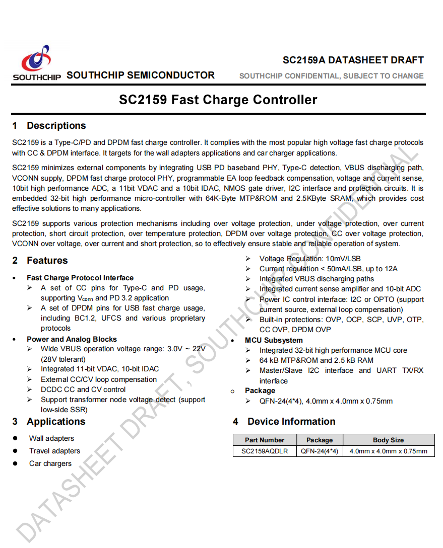
Here is the information about SouthChip SC2159A.
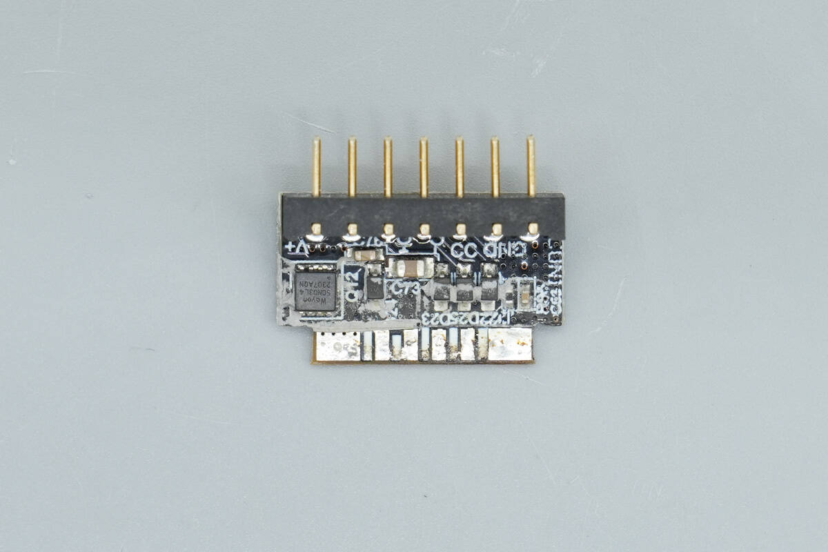
The small PCB has one side soldered with the connector socket and the VBUS MOSFET.
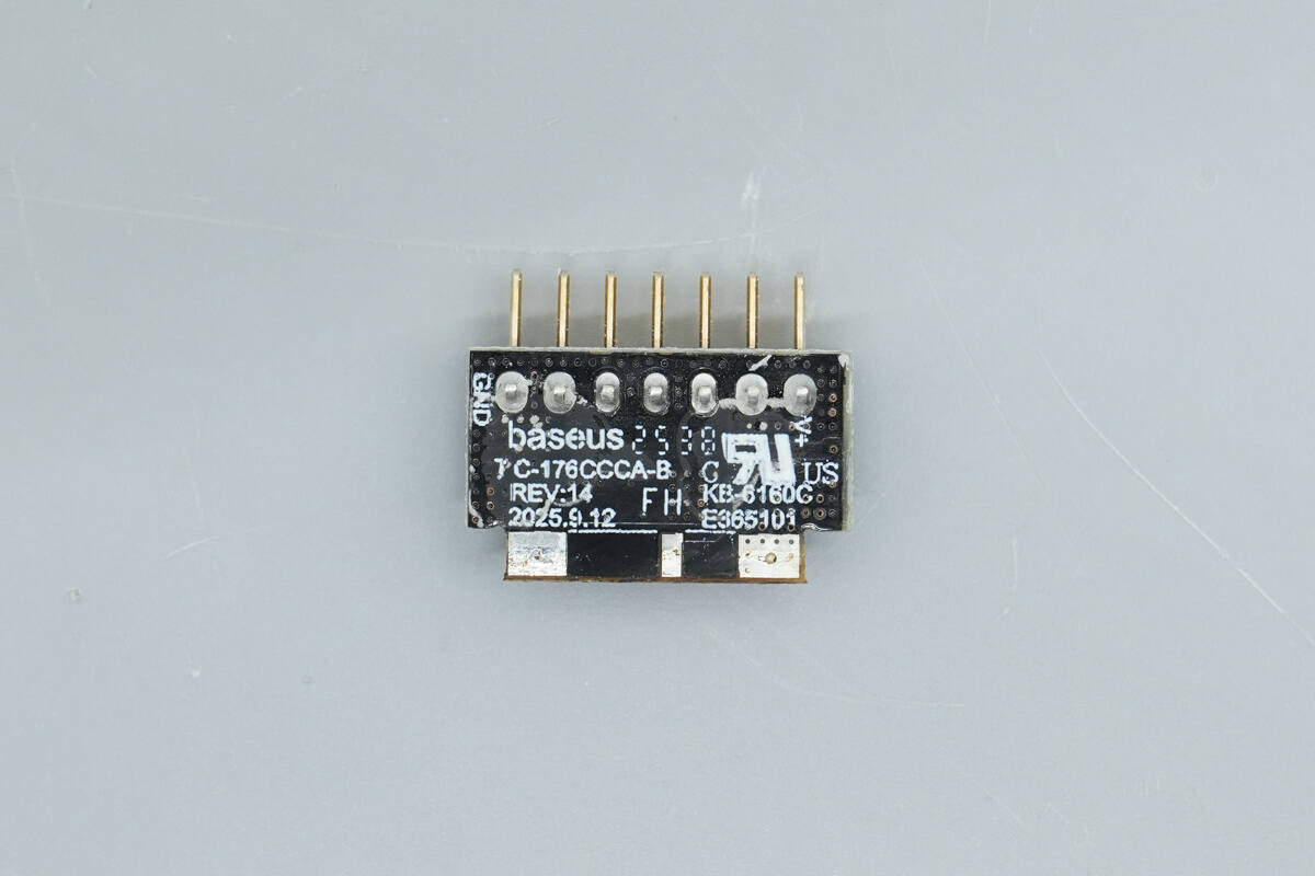
The other side of the PCB is printed with the Baseus logo.
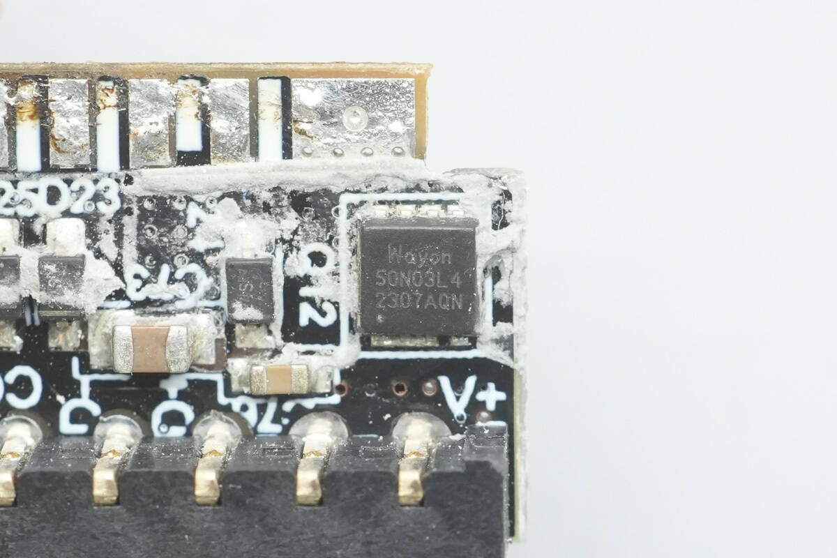
The VBUS MOSFET from WAYON, model WMQ50N03LG4, is an NMOS with a voltage rating of 30V and an on-resistance of 4.2mΩ. It comes in a PDFN3030-8L package.
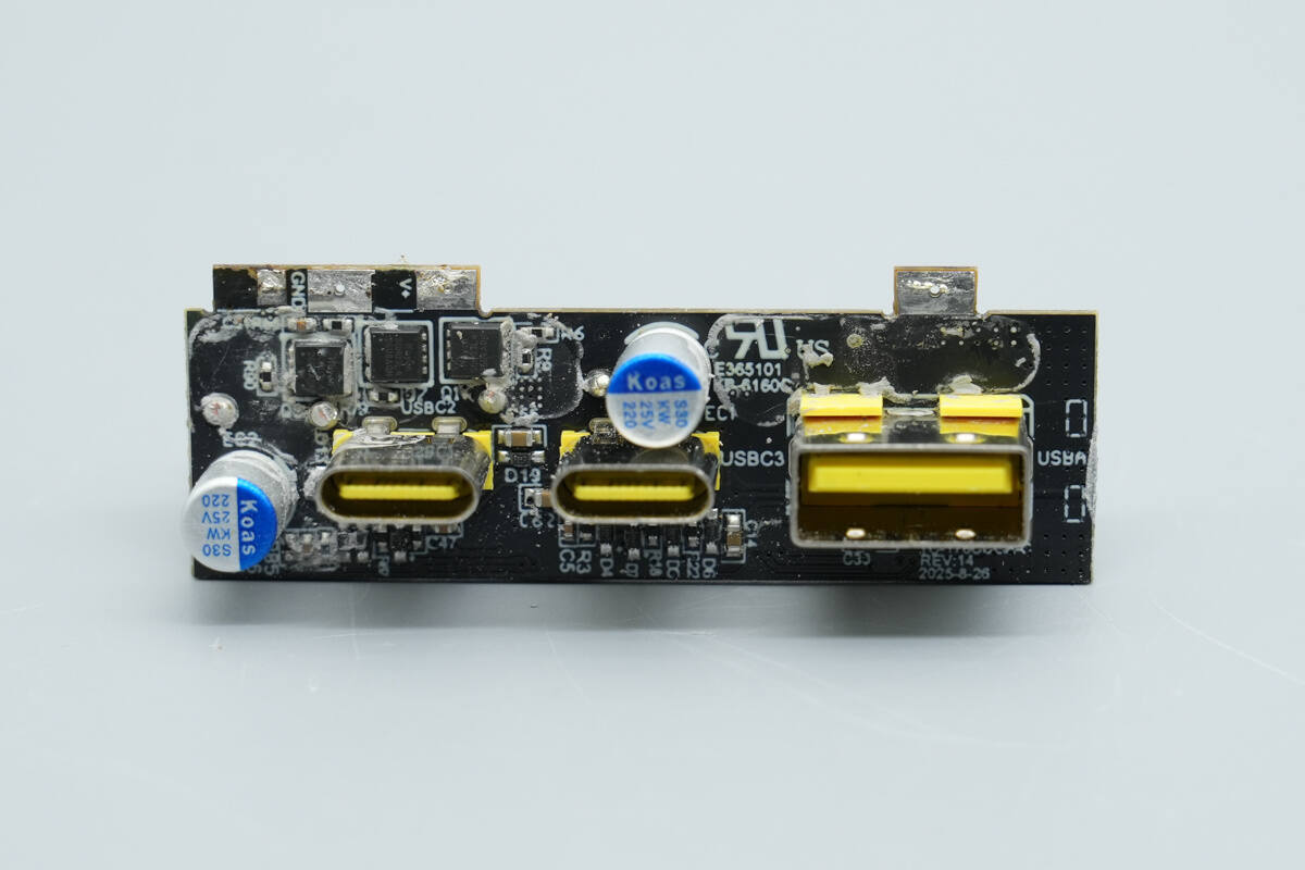
The front side of the buck PCB features synchronous buck MOSFETs, VBUS MOSFETs, USB-C and USB-A sockets, as well as solid capacitors.
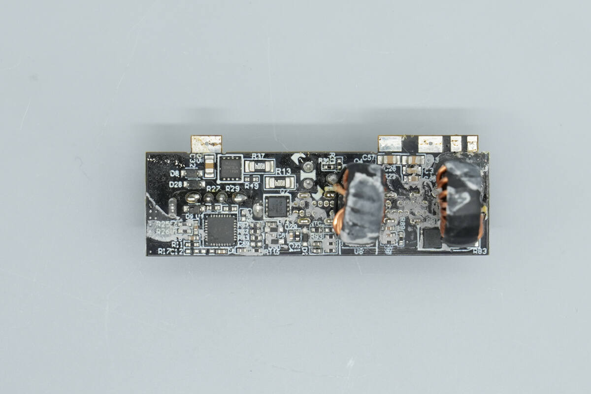
The backside of the PCB is soldered with the buck protocol chips, VBUS MOSFETs, and buck inductors.
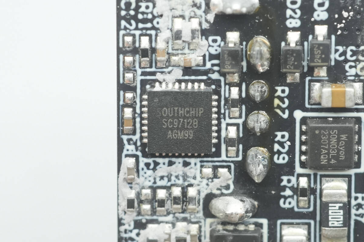
The buck protocol chip for two USB-C interfaces from SouthChip, model SC9712B, is a highly integrated dual-port fast charging SoC. It incorporates a 36V efficient synchronous buck controller, along with one Type-C interface and two DPDM fast charging protocol interfaces, supporting the UFCS fast charging protocol. The SC9712B supports dual-chip cooperation, allowing full-power output when working in single-port mode, and automatically distributing power when both ports are active. It operates without the need for MCU control.
The SC9712B supports a total output power of up to 140W, with both ports supporting CC/CV modes, NTC temperature monitoring, and a variety of protection mechanisms, including over-voltage, over-current, short-circuit, and over-temperature protections, effectively safeguarding the chip and the system. It comes in a QFN-32 package.
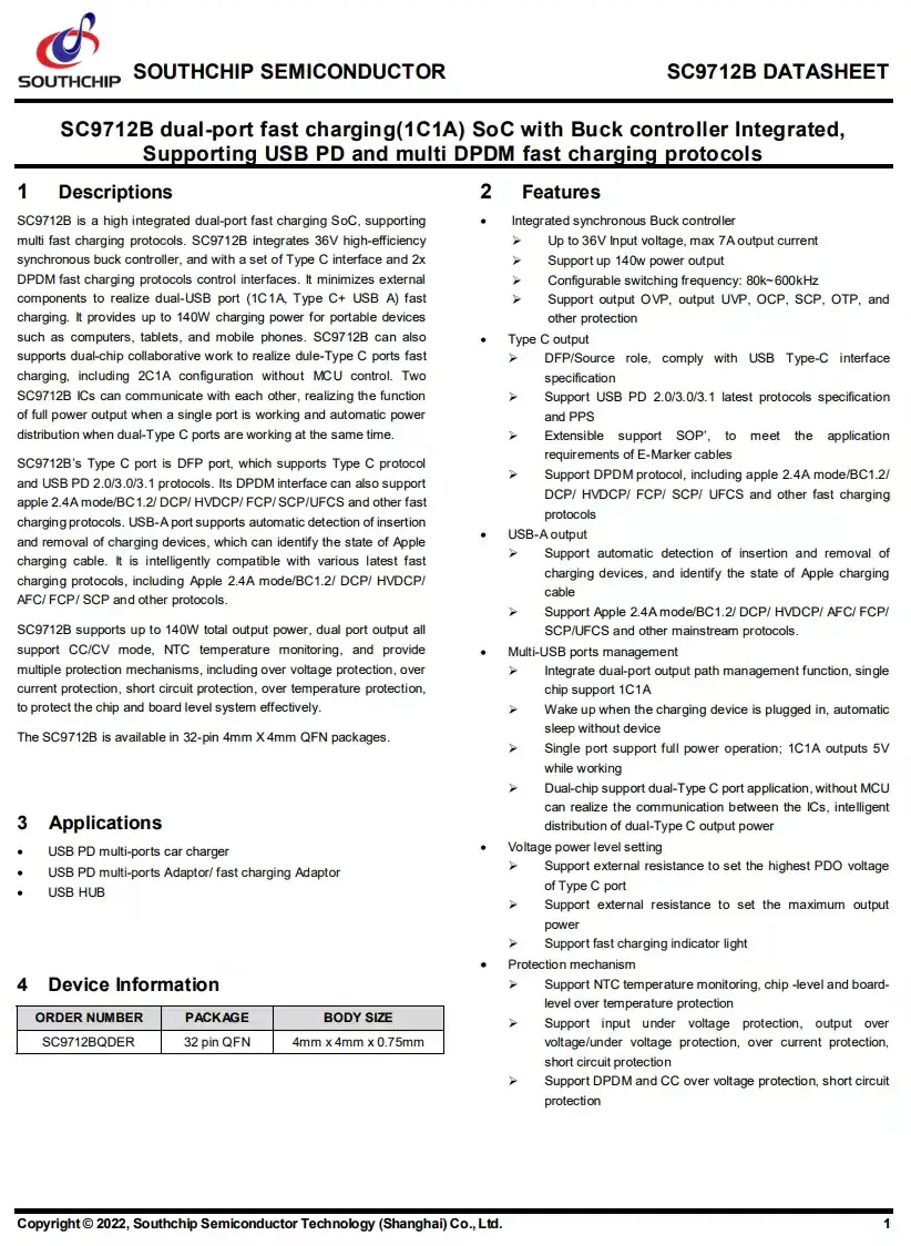
Here is the information about SouthChip SC9712B.
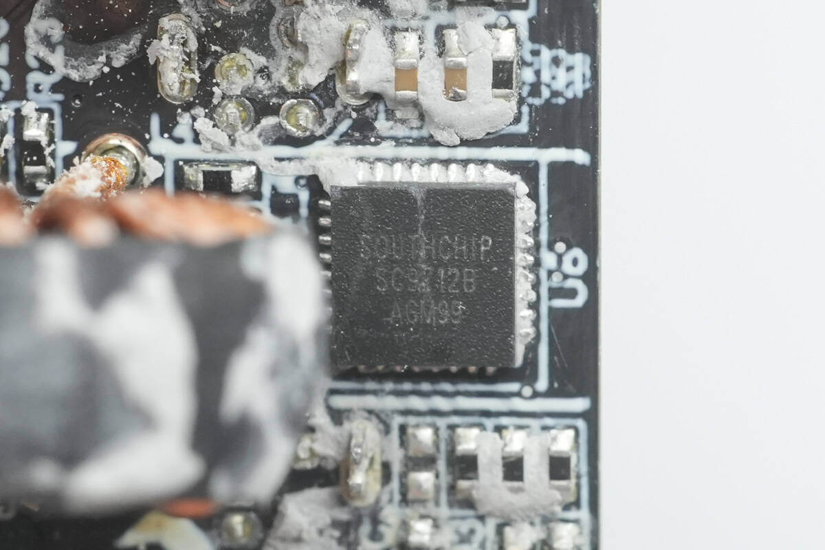
The other channel also uses the SouthChip SC9712B buck protocol chip.
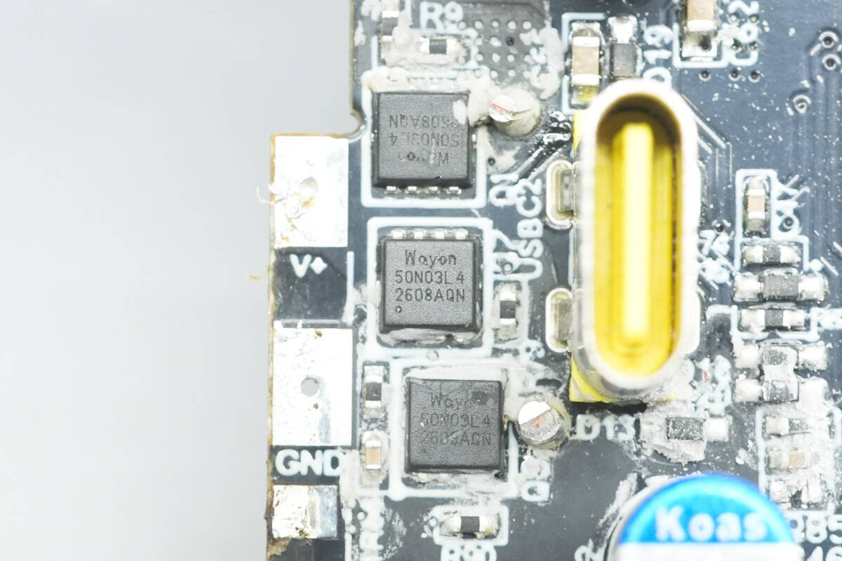
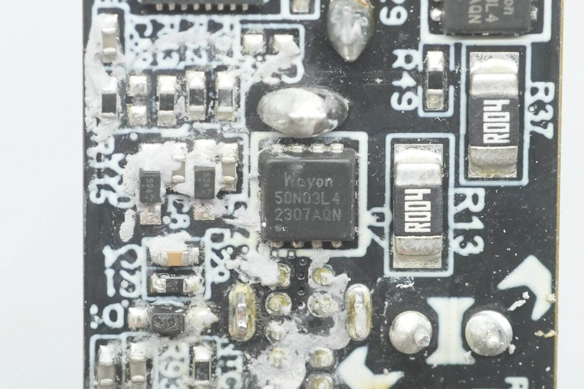
The synchronous buck MOSFETs use WAYON WMQ50N03LG4.
The backside features a buck MOSFET of the same model.
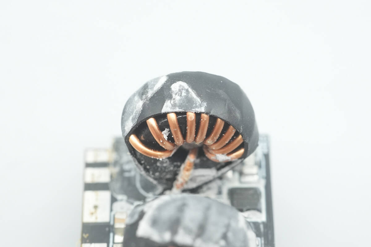
The buck inductor is wound with enameled wire and insulated with a heat-shrink tube.
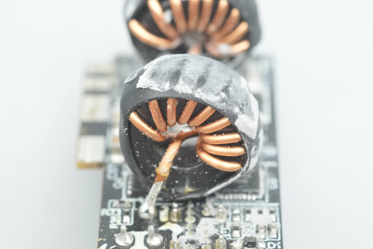
Close-up of the other buck inductor.
The filter capacitor is from Koshin, with a specification of 25V, 220μF.
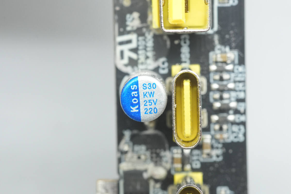
The other filter capacitor has the same specification.
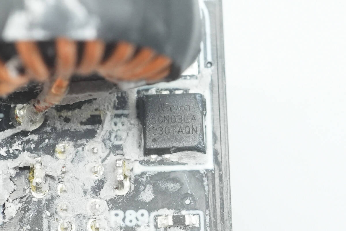
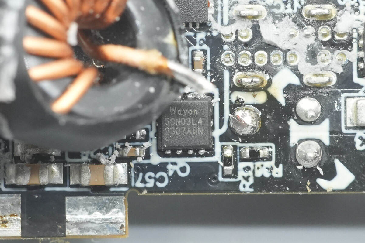
The VBUS MOSFET uses WAYON WMQ50N03LG4.
The VBUS MOSFET uses WAYON WMQ50N03LG4.
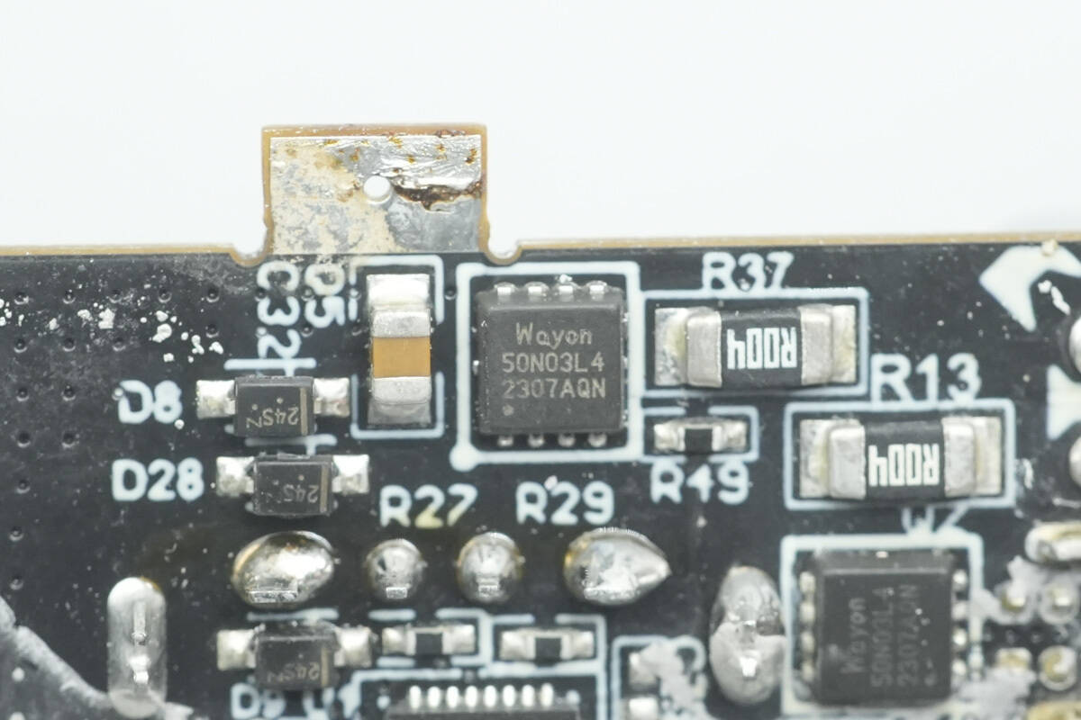
The USB-A interface VBUS MOSFET uses WAYON WMQ50N03LG4.
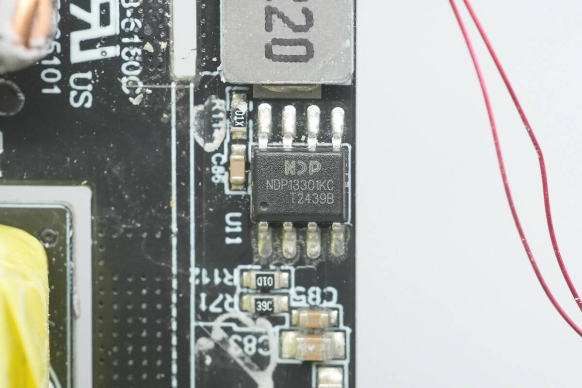
The synchronous buck chip from NDP, model NDP1330KC, features an integrated MOSFET and supports an input voltage range of 7–30V. It provides an output current of up to 3.5A and includes constant voltage and constant current control. The chip supports 100% duty cycle, has adjustable line loss compensation, and operates at a switching frequency of 130kHz. It comes in an SOP8 package.
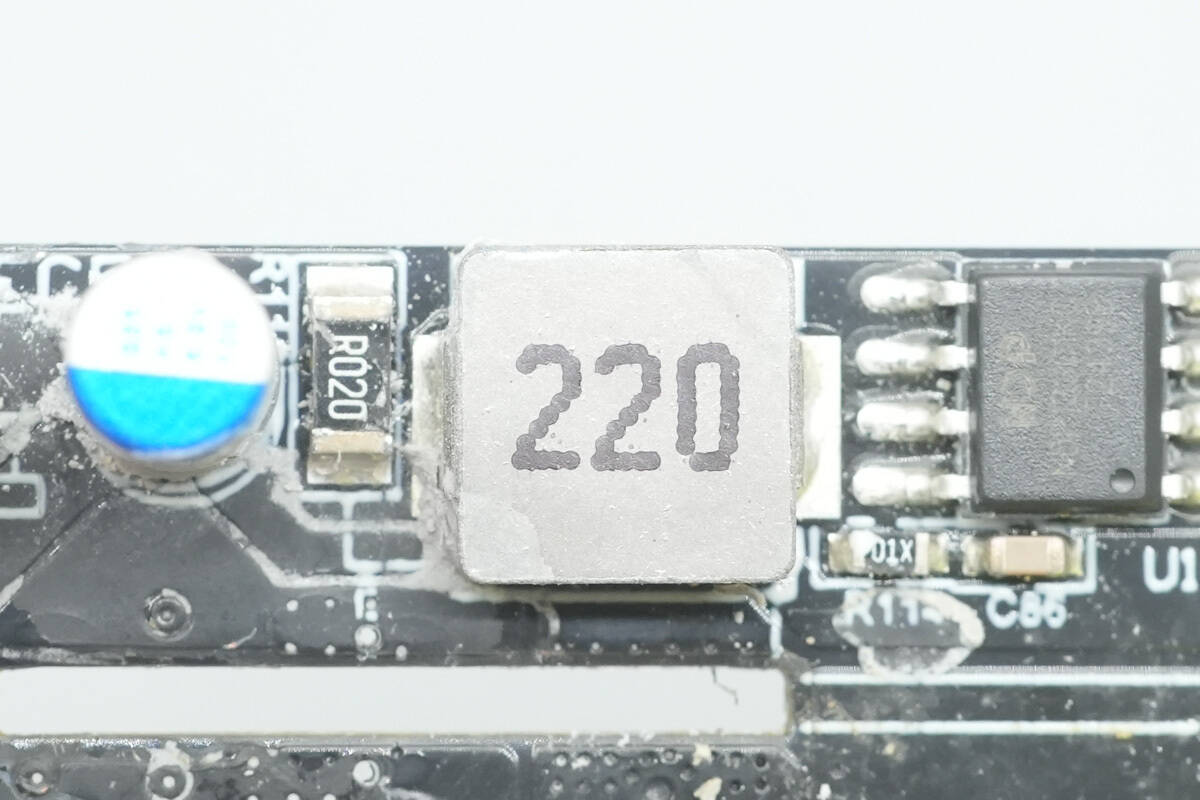
Close-up of the 22μH buck inductor.
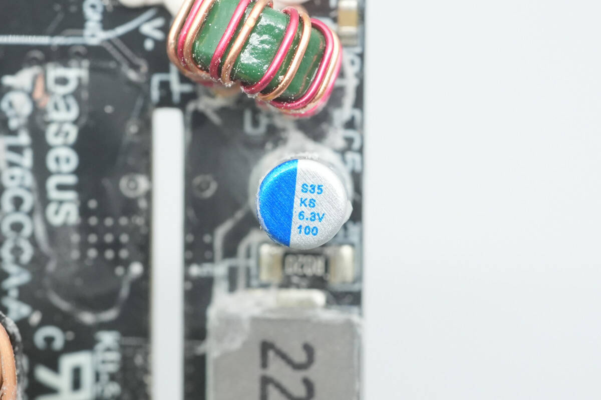
The filter capacitor is from Koshin, with a specification of 6.3V, 100μF.
The filter inductor is wound with enameled wire.
Close-up of the thermistor.
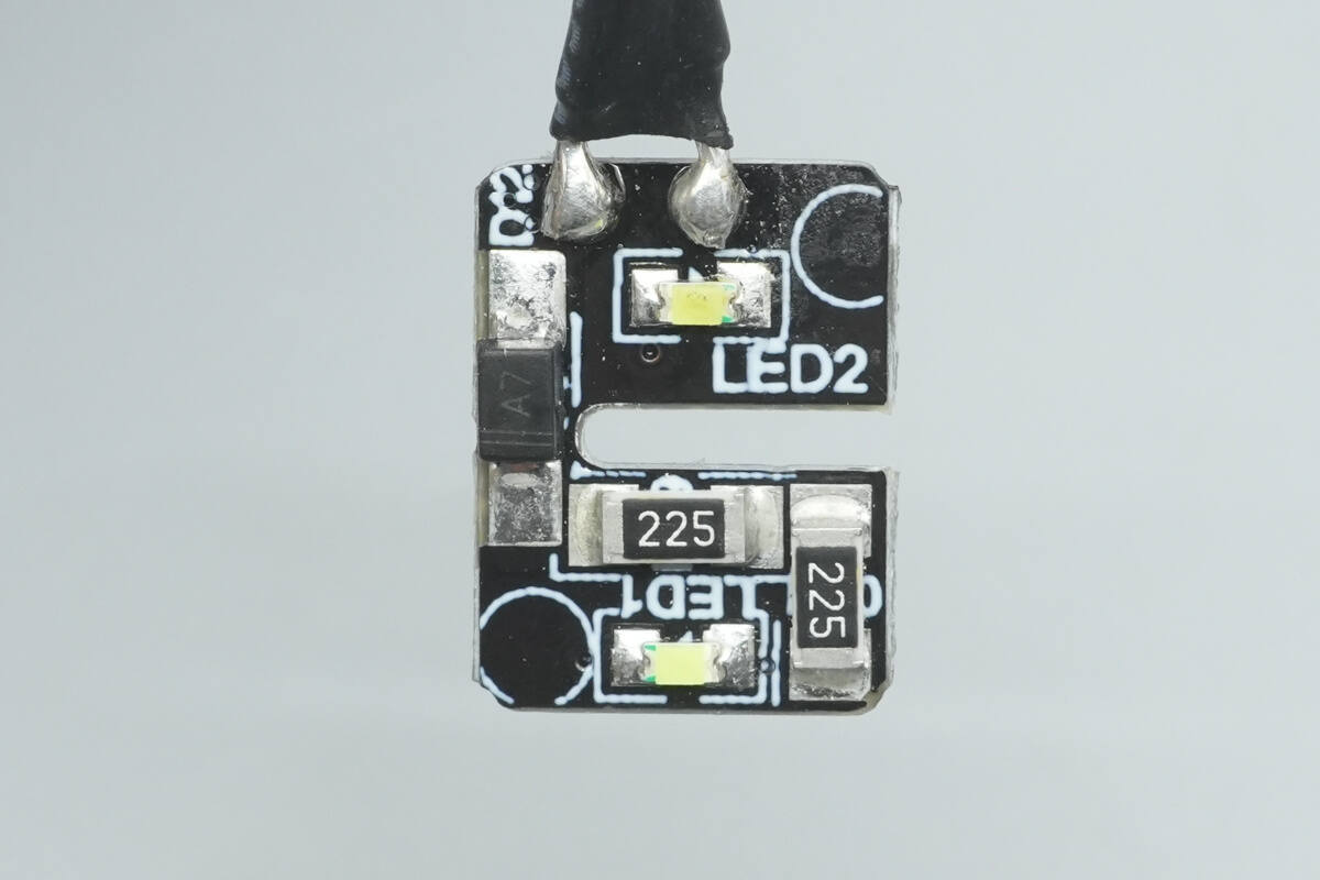
The power indicator light and surge protection indicator light are soldered onto a separate PCB.
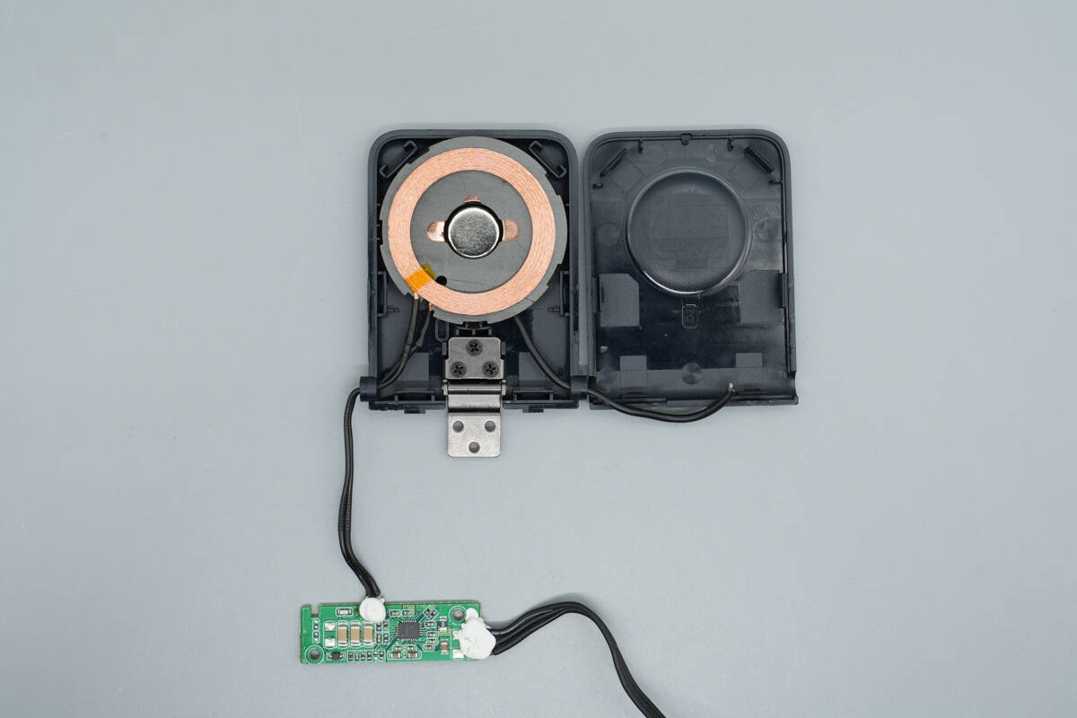
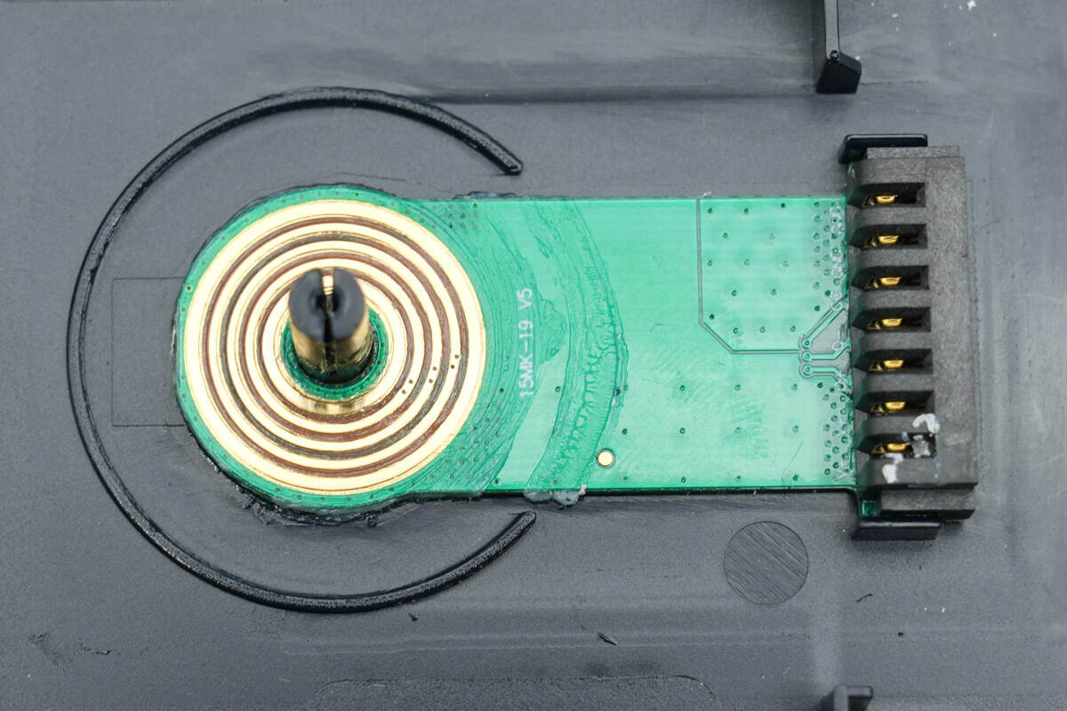
After opening the wireless charging pad casing, the interior features a shaft and a wireless charging coil.
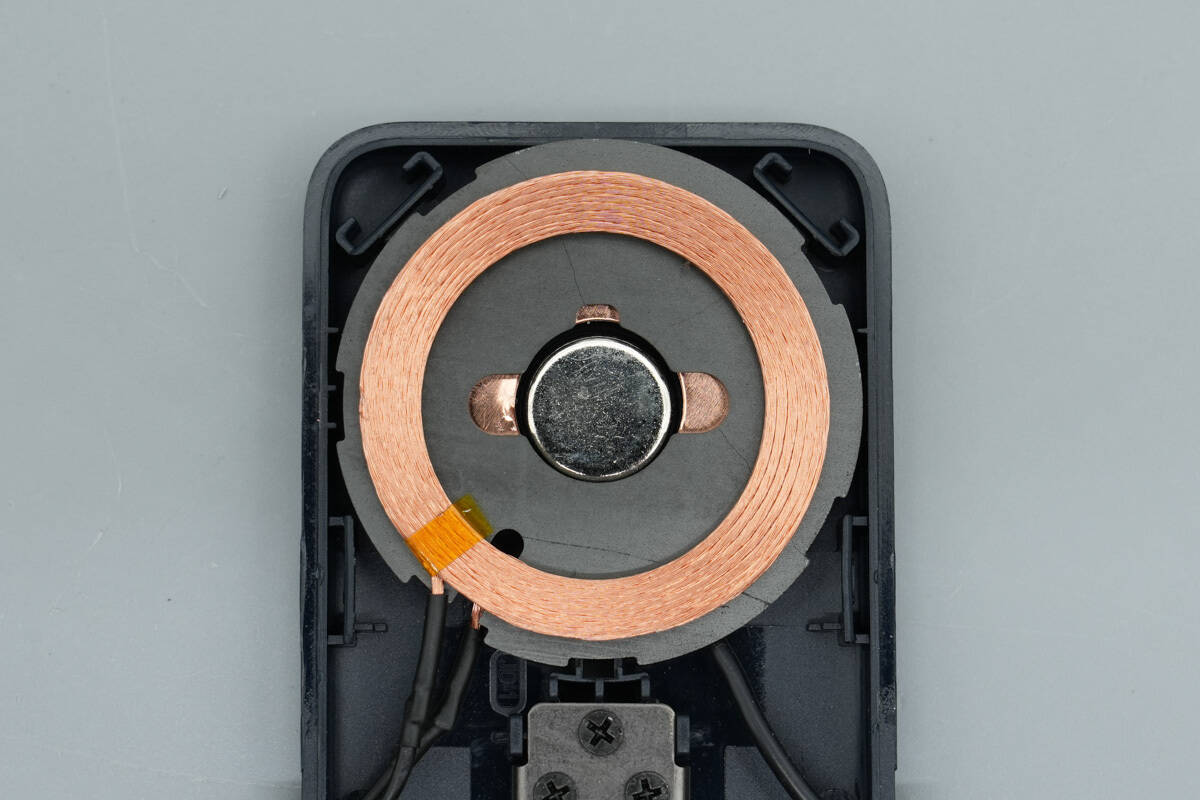
The coil is wound with Litz wire, and a magnet is placed in the center for attaching the smartwatch.
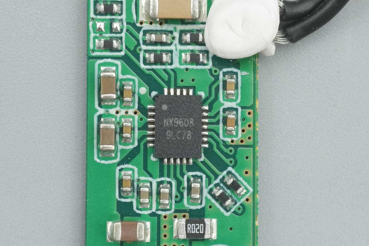
The wireless charging chip is marked with NX9608 and comes in a QFN24 package.
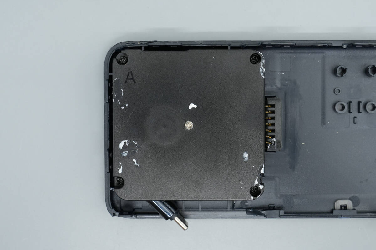
The retractable cable module casing is secured with screws.
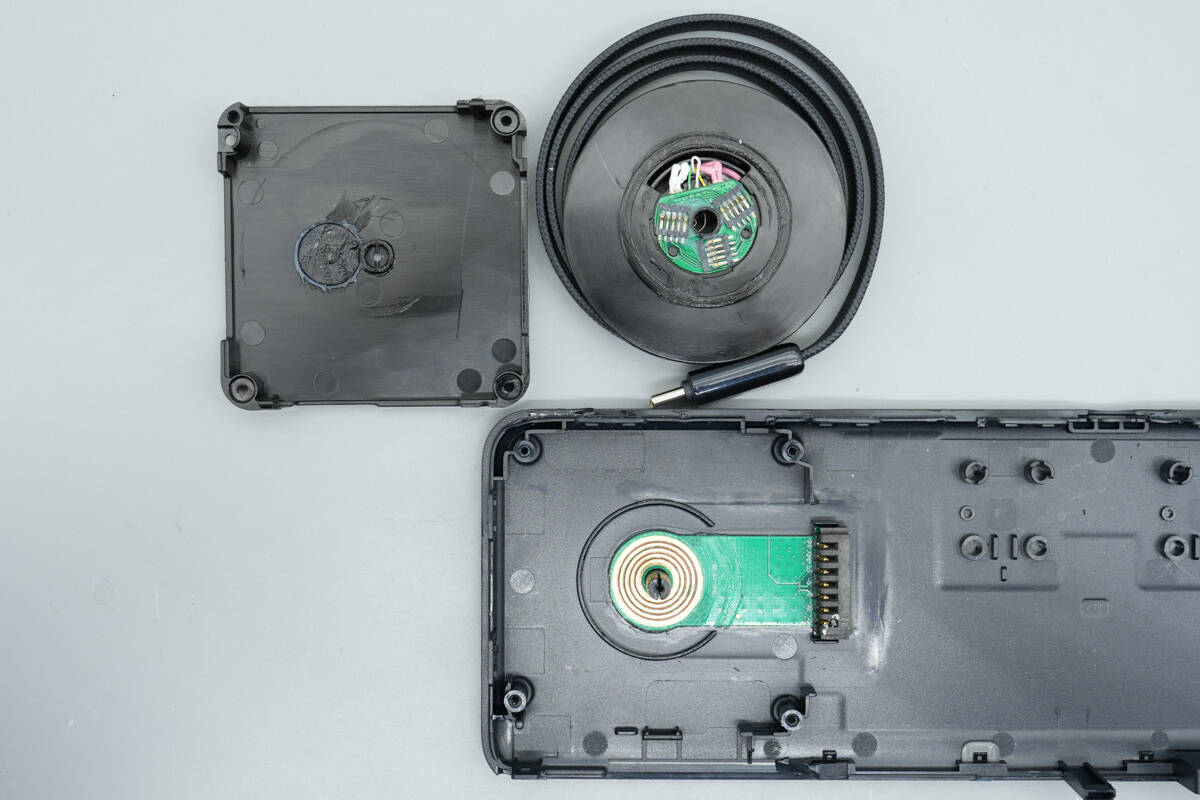
Remove the spool.
Inside, there is a PCB slip ring.
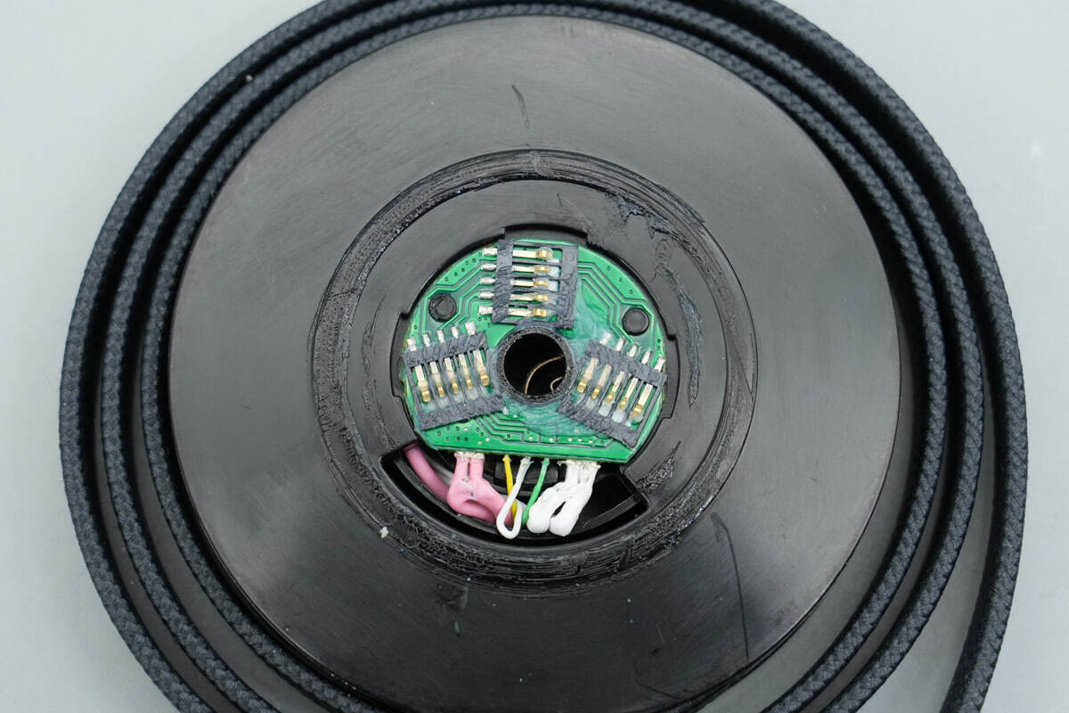
The spool is equipped with three brushes.
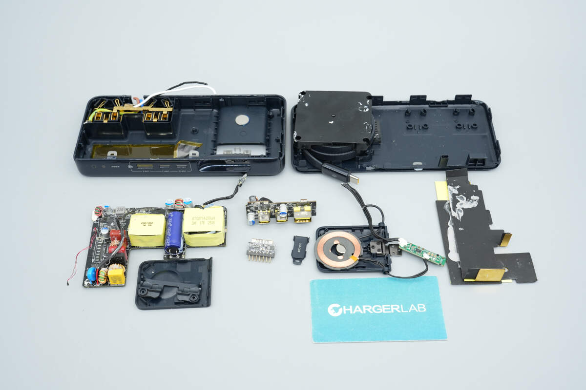
Well, those are all components of the Baseus 100W 7-in-1 Charging Station.
Summary of ChargerLAB
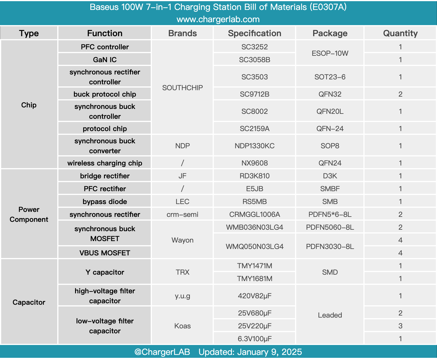
Here is the component list of the Baseus 100W 7-in-1 Charging Station for your convenience.
It is officially authorized by Huawei’s protocol and supports Huawei 66W Super Fast Charging, as well as wireless charging for smartwatches. The device features two five-pin output sockets, a built-in USB-C cable, two USB-C ports, and one USB-A port. Both USB-C ports support 100W output.
After taking it apart, we found that it uses a strong and weak power independent partition architecture and is equipped with surge protection. The fast-charging circuit employs SouthChip SC3252 and SC3058B GaN ICs for PFC boost and flyback conversion. The synchronous rectifier controller is the SC3503.
The built-in USB-C cable uses the SouthChip SC8002 synchronous buck controller paired with the SC2159A protocol chip. The two USB-C ports utilize the SC9712B buck protocol chip, and the NDP1330KC synchronous buck chip is used to provide power for wireless charging of the smartwatch. Both the front and back sides of the PCBA module are filled with glue, and it is equipped with a brass heatsink to enhance heat dissipation, ensuring solid and reliable craftsmanship and materials.
Related Articles:
1. Teardown of MIIIW 45W Mini Magic Cube GaN Charger (iCA4501)
2. Teardown of AOHi THE FUTURE AI PD GaN+ 170W 3-Port LED Display Fast Car Charger (AOC-S009)
3. Teardown of Torras FlexLine 67W Charger (CQ10)