Introduction
Anker has launched a new Thunderbolt 5 desktop docking station featuring 14 ports. It includes one Thunderbolt 5 upstream port and two Thunderbolt 5 downstream ports, with a single-port data transfer rate of 80 Gbps and a shared bandwidth of 120 Gbps for dual ports. The HDMI and DisplayPort interfaces support 8K 60Hz output and enable triple extended display.
The dock comes with a built-in GaN power supply, delivering a total output of 250W. On the front of the device, there are two USB-C ports and one USB-A port. Each of the USB-C ports supports up to 45W power output. On the back, there are Thunderbolt 5 ports, HDMI, DisplayPort, a 2.5G Ethernet port, and additional USB-A ports, which are ideal for connecting devices that don’t need frequent plugging and unplugging, keeping your desktop clean and organized.
At the top of the dock, there is an ambient light ring that uses dynamic lighting effects to indicate the operating status of the dock. The rear Thunderbolt 5 port supports 140W power output, providing fast charging for laptops. Inside, the dock is equipped with an active cooling fan to dissipate heat generated during operation, helping unleash its full performance.
Now, let’s take a closer look at the teardown of this Thunderbolt 5 dock to explore its internal design and components.
Product Appearance
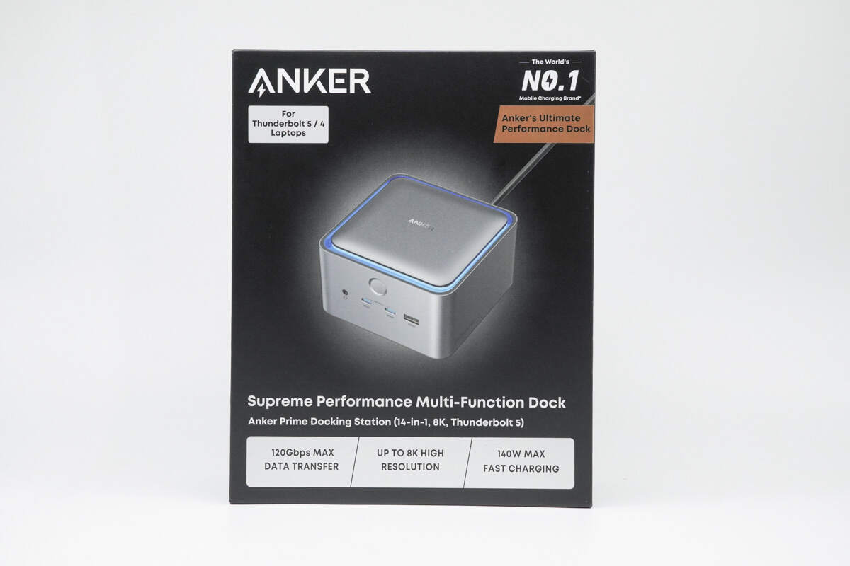
ANKER, the dock's appearance, name, and selling points are printed on the front of the box.
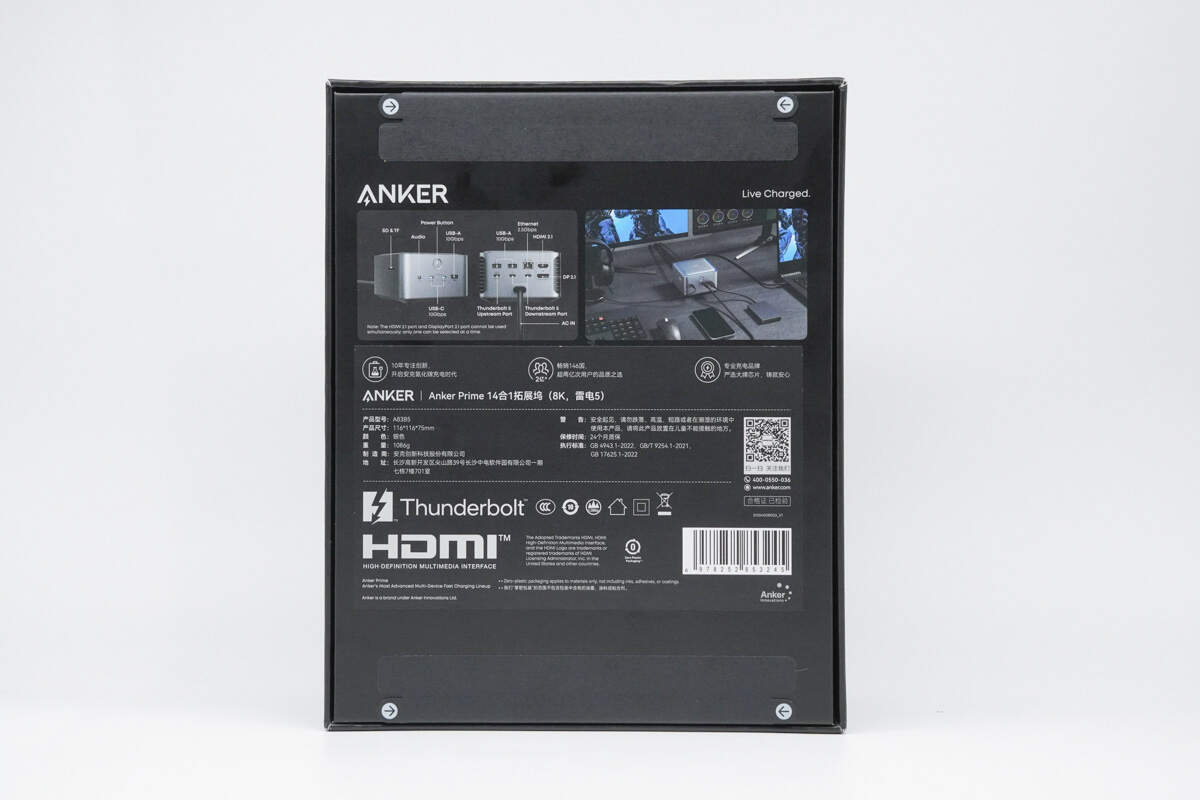
The port names and corresponding functions are marked on the back, as well as the usage scenarios and product selling points.
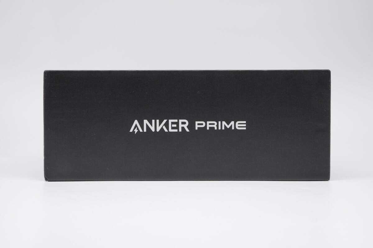
ANKER PRIME is printed on the side of the box.
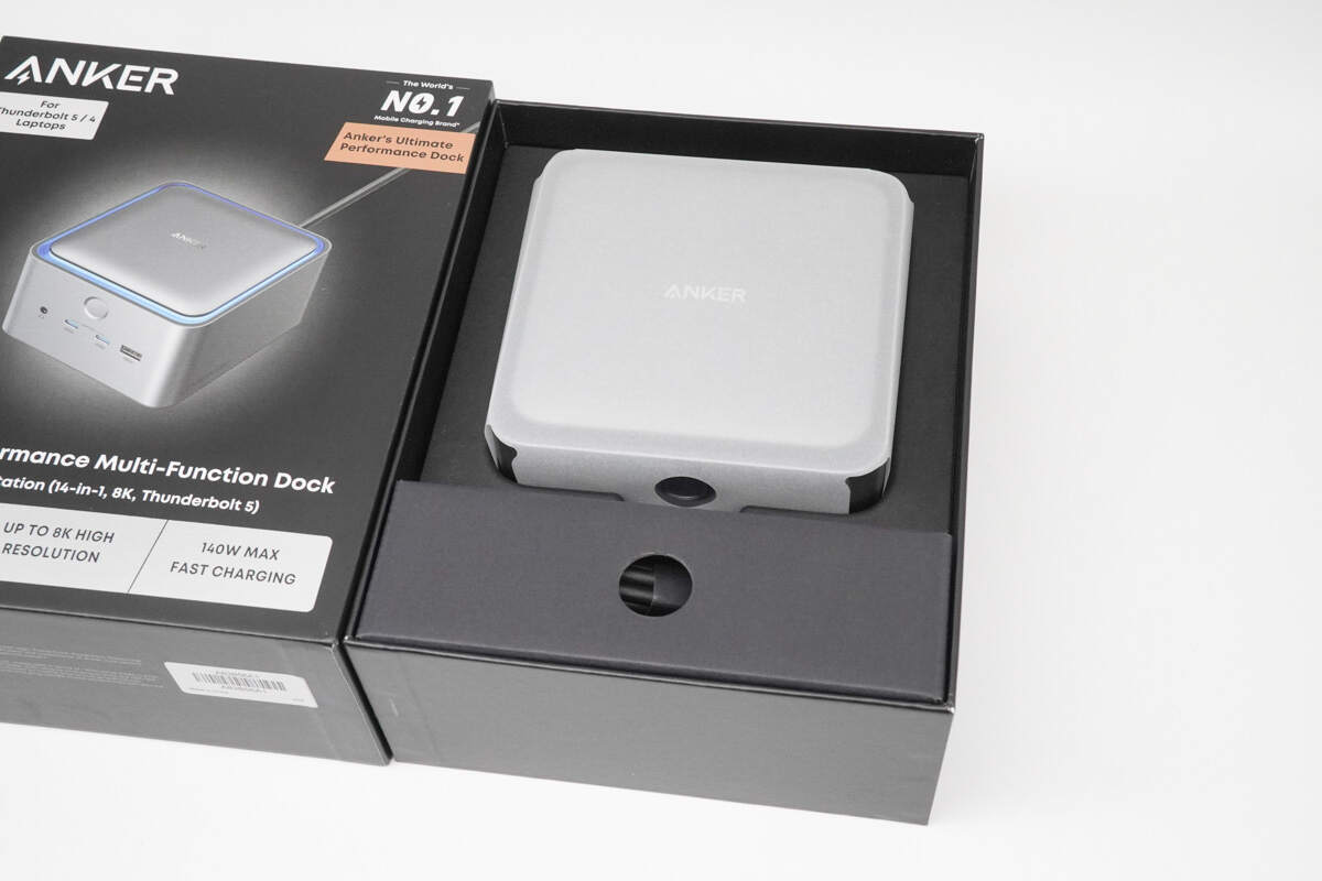
Open the box, and you will see the dock is wrapped in paper.
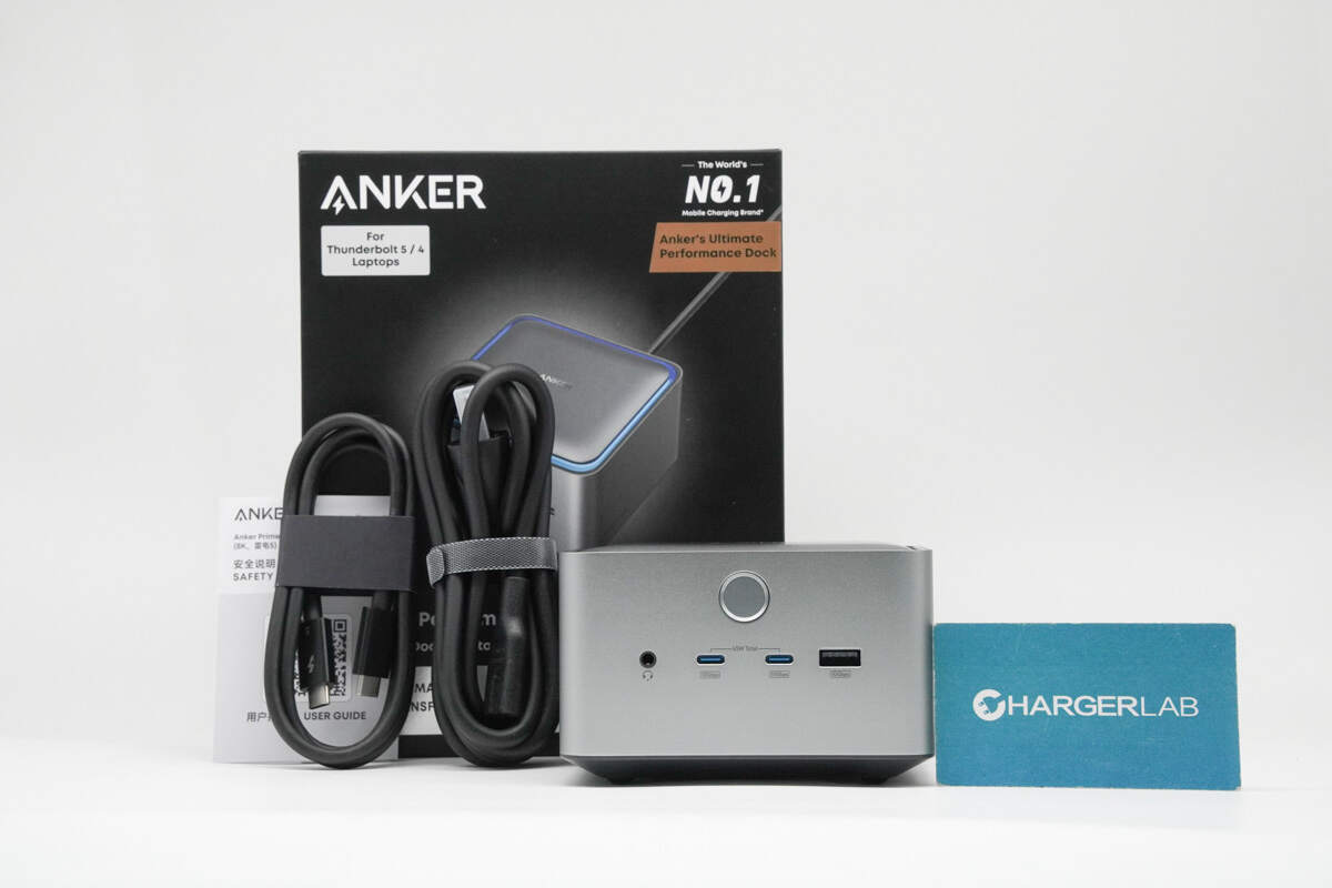
The box includes the dock, a Thunderbolt 5 data cable, a power cable, and some documents.
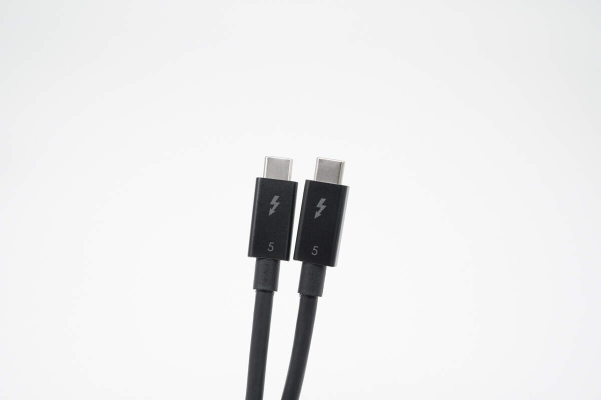
The included Thunderbolt 5 data cable uses a dual USB-C design.
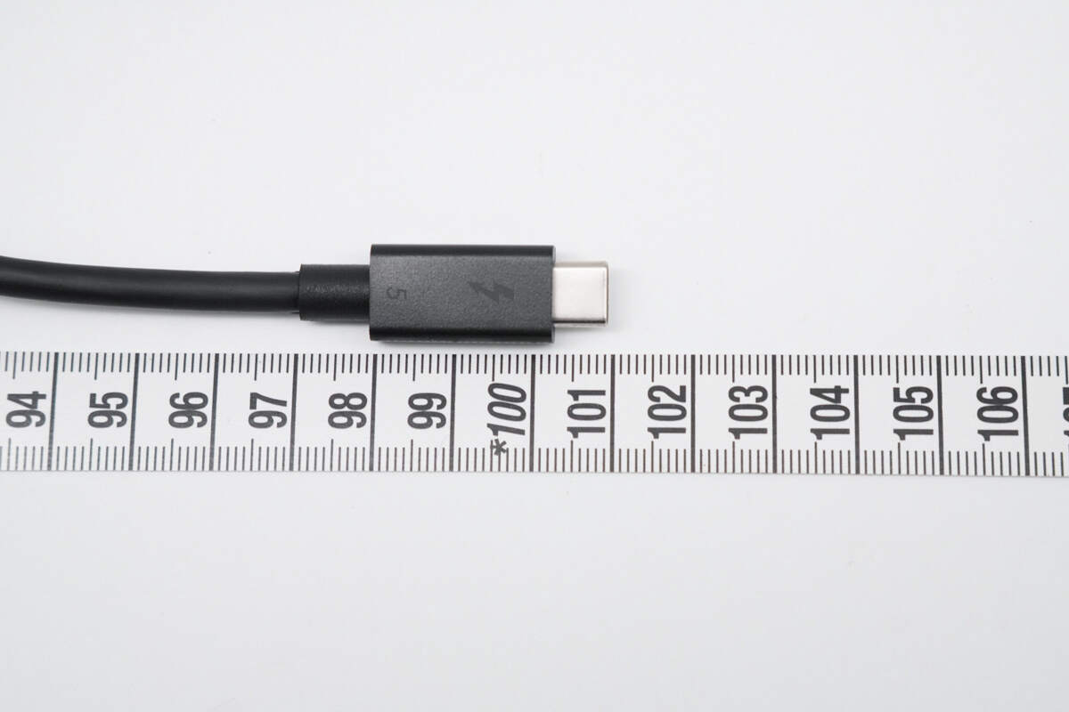
The length of the cable is about 1 m (3' 3.37'').
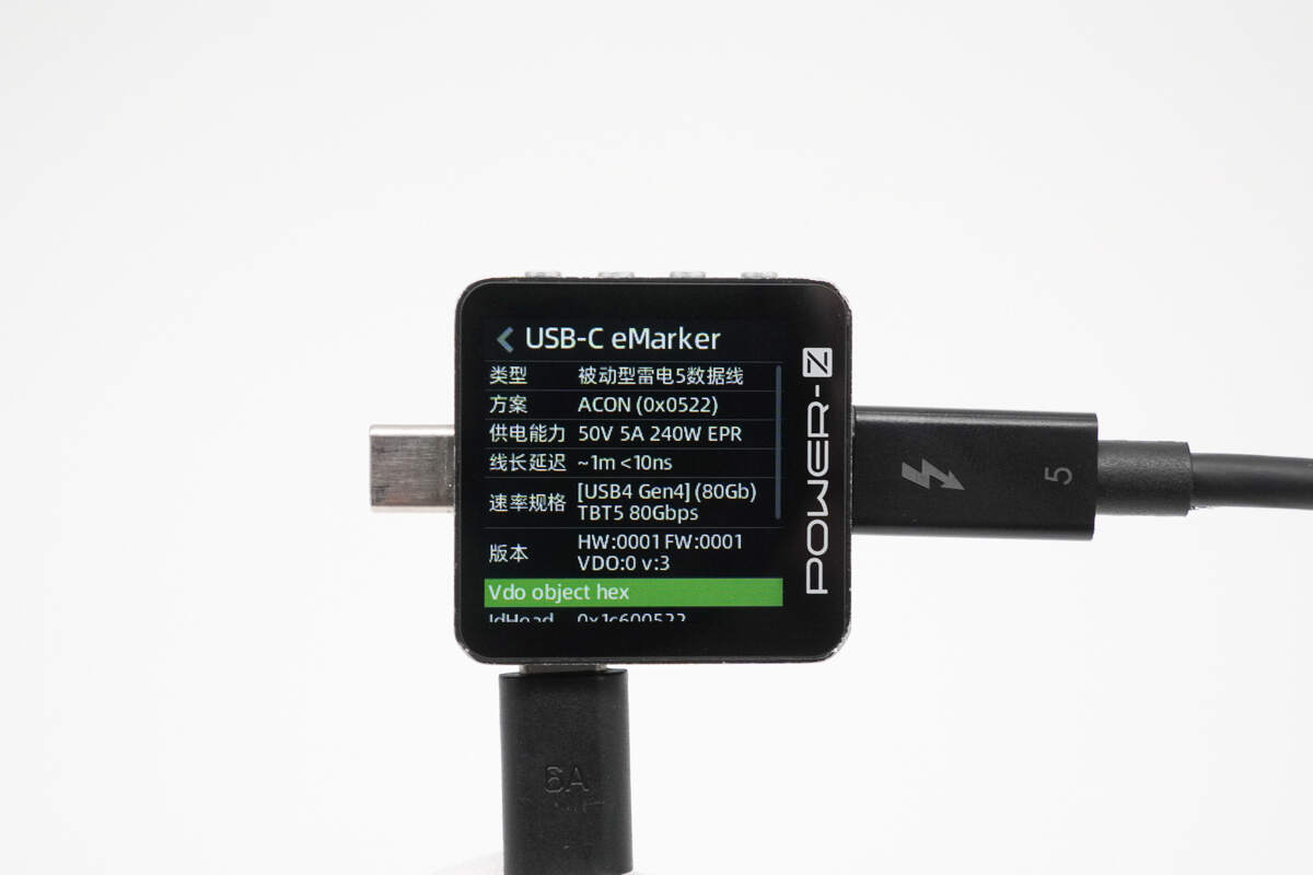
ChargerLAB POWER-Z KM003C shows it has an E-marker chip. It supports power delivery up to 50V/5A and data transfer capabilities of USB4 Gen4 (80Gbps) and Thunderbolt 5 at 80Gbps.
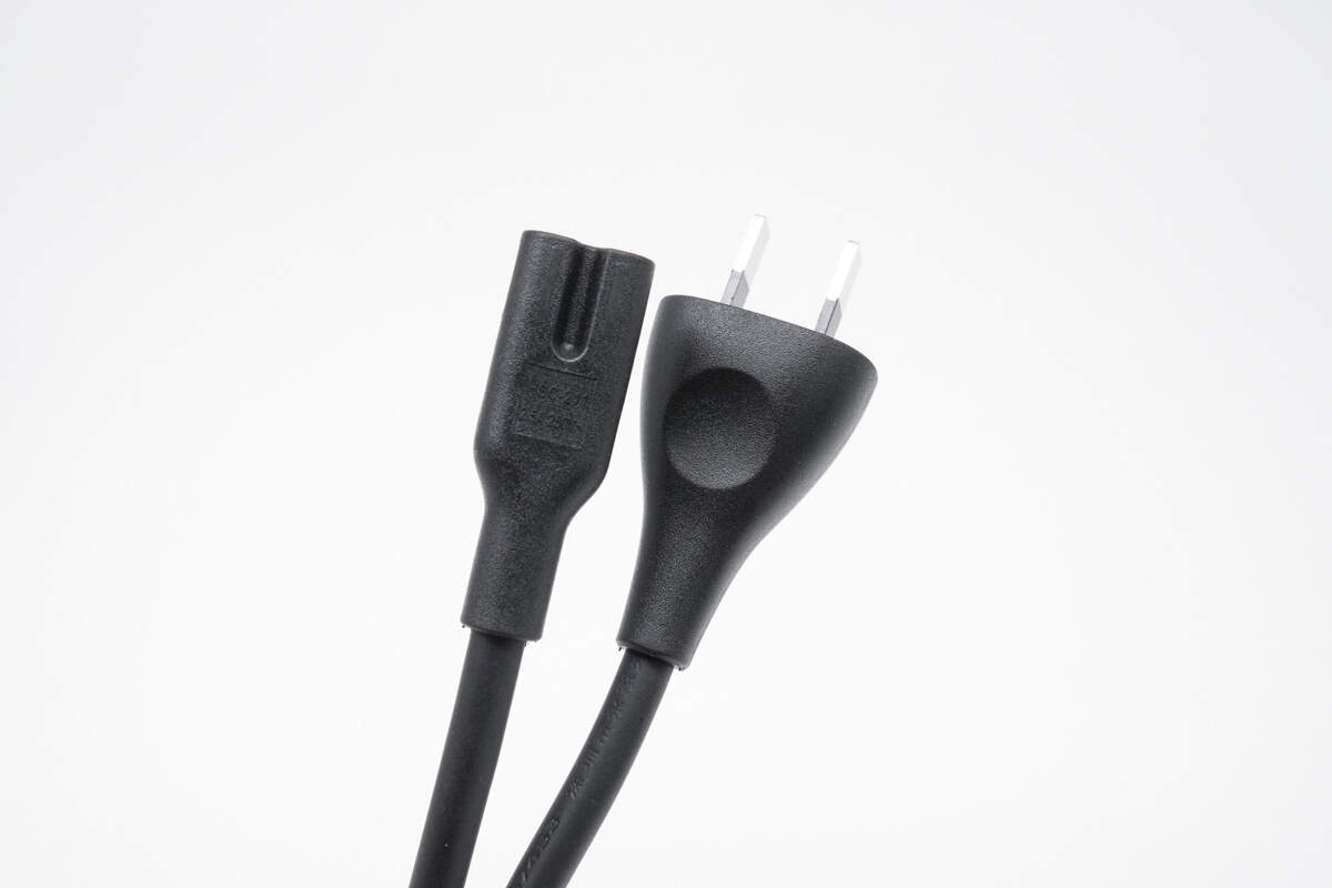
The included power cord features a two-prong plug and a C7 connector on the other end.
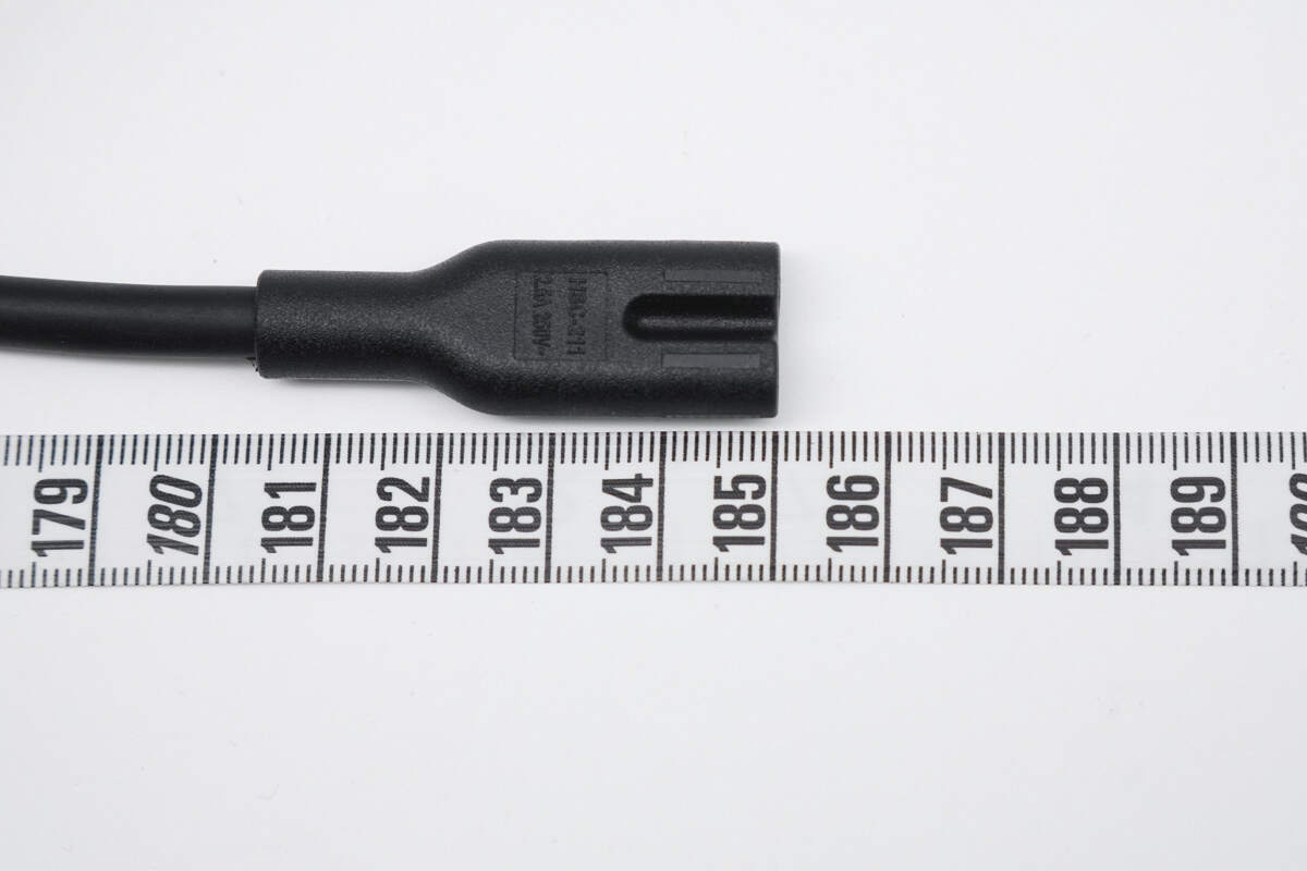
The length of the power cord is 185 cm (6' 0.8'').
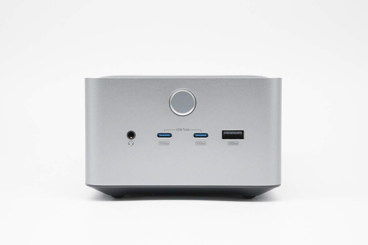
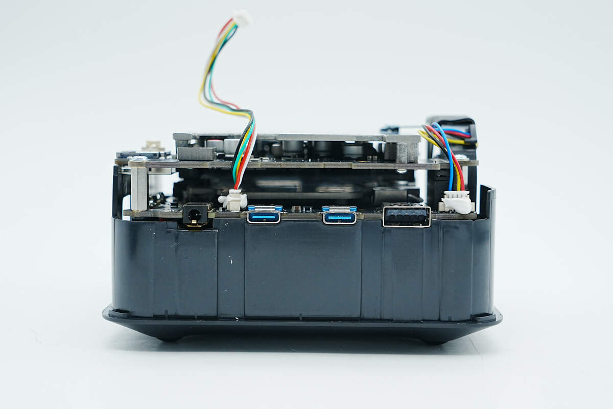
On the front, there is a power button, a 3.5mm headphone jack, two USB-C ports, and one USB-A port.
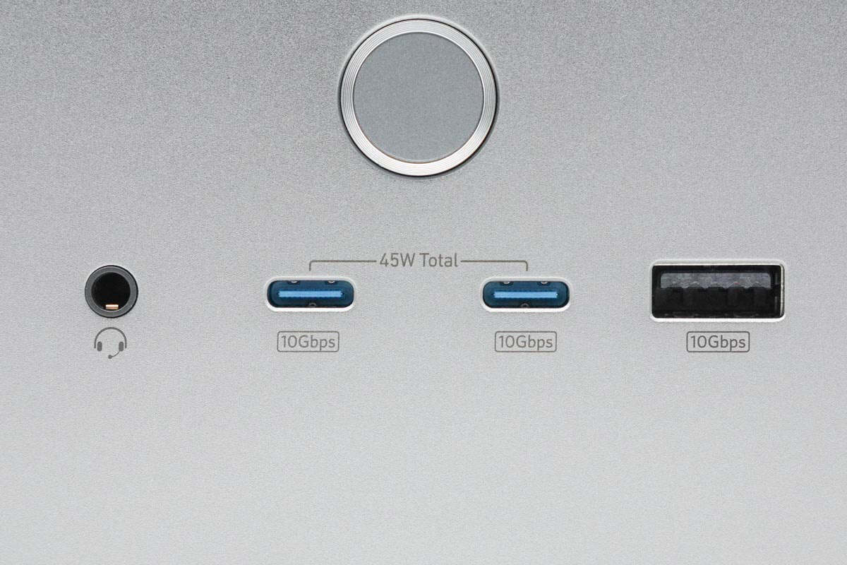
Above the USB-C ports, it is indicated that the two ports share a total output power of 45W. All three USB ports support data transfer speeds of up to 10 Gbps.
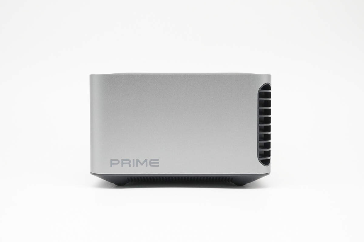
PRIME is printed on this side.
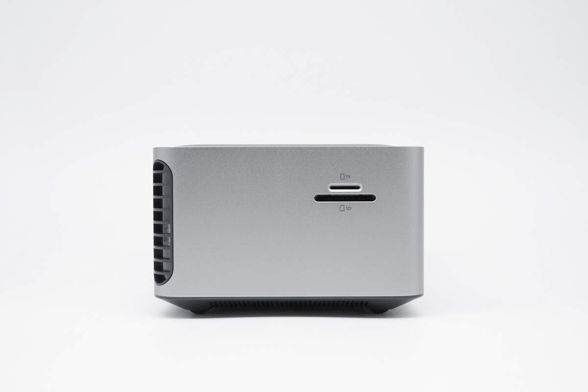
On the other side, there are TF and SD card slots.
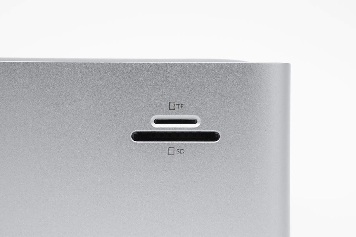
The card slot area is labeled with clear markings.
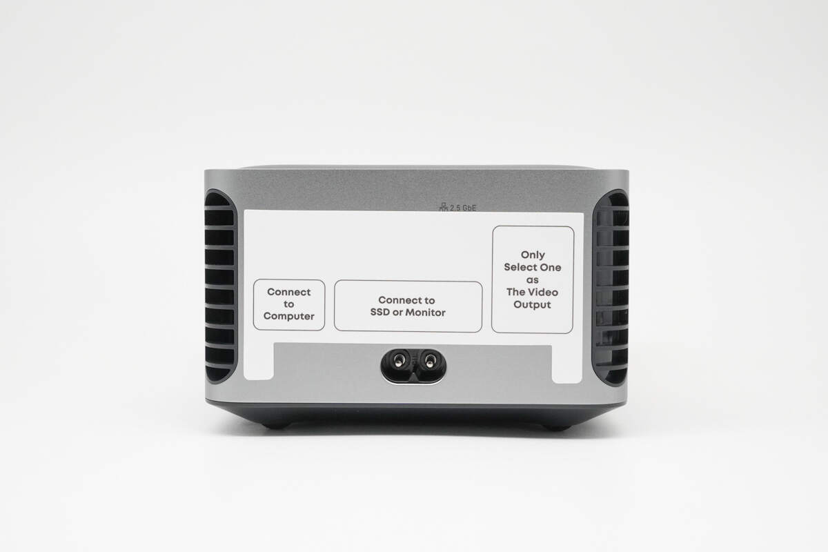
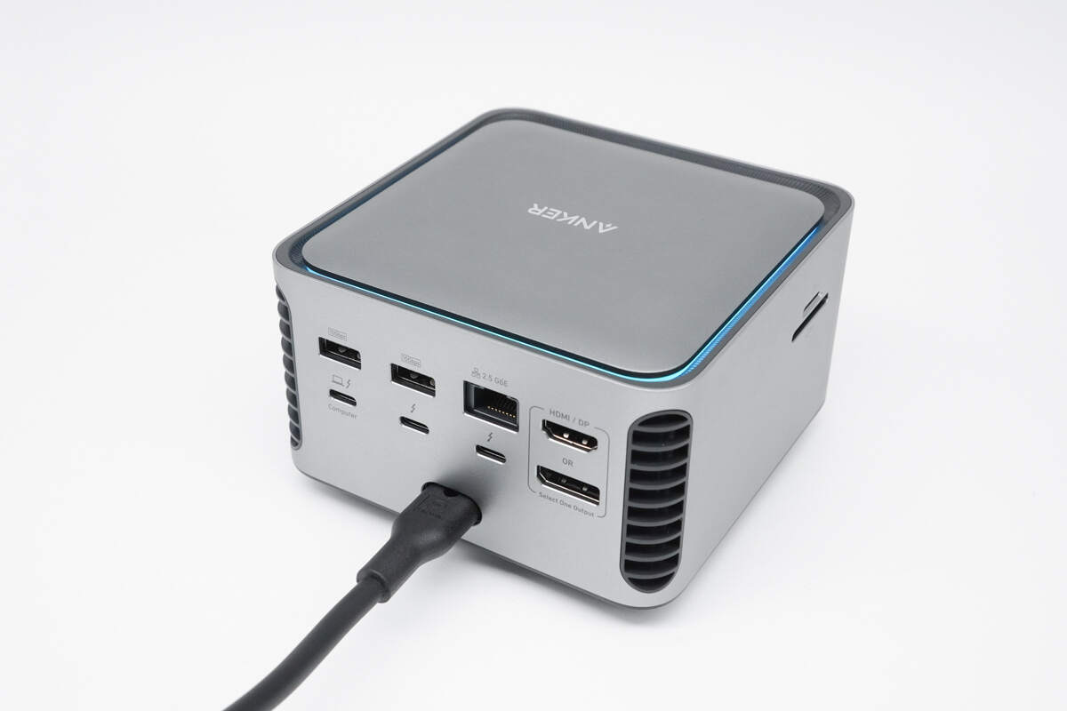
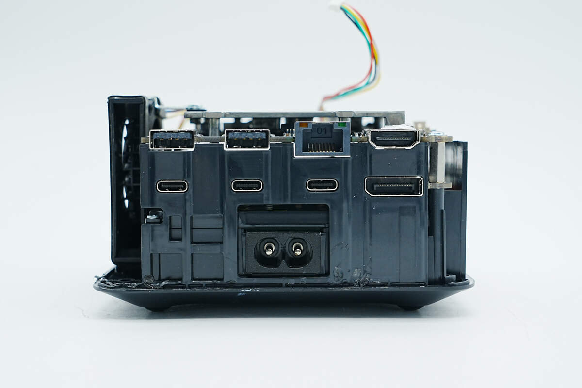
The sticker on the back labels the functions of each port.
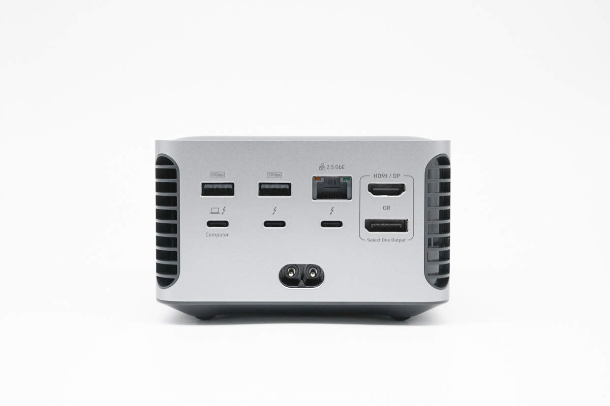
Here's the complete list of rear ports:
- Two Thunderbolt 5 downstream ports (each supporting up to 80 Gbps, with a combined bandwidth of 120 Gbps)
- One Thunderbolt 5 upstream port (supporting up to 140W power delivery)
- One HDMI port
- One DP port
- One 2.5G Ethernet port
- Two USB-A ports (supporting up to 10 Gbps data transfer)
- DC input port (for power supply)
This comprehensive set of ports ensures versatile connectivity options for various devices and peripherals.
The top of the dock features the ANKER logo.
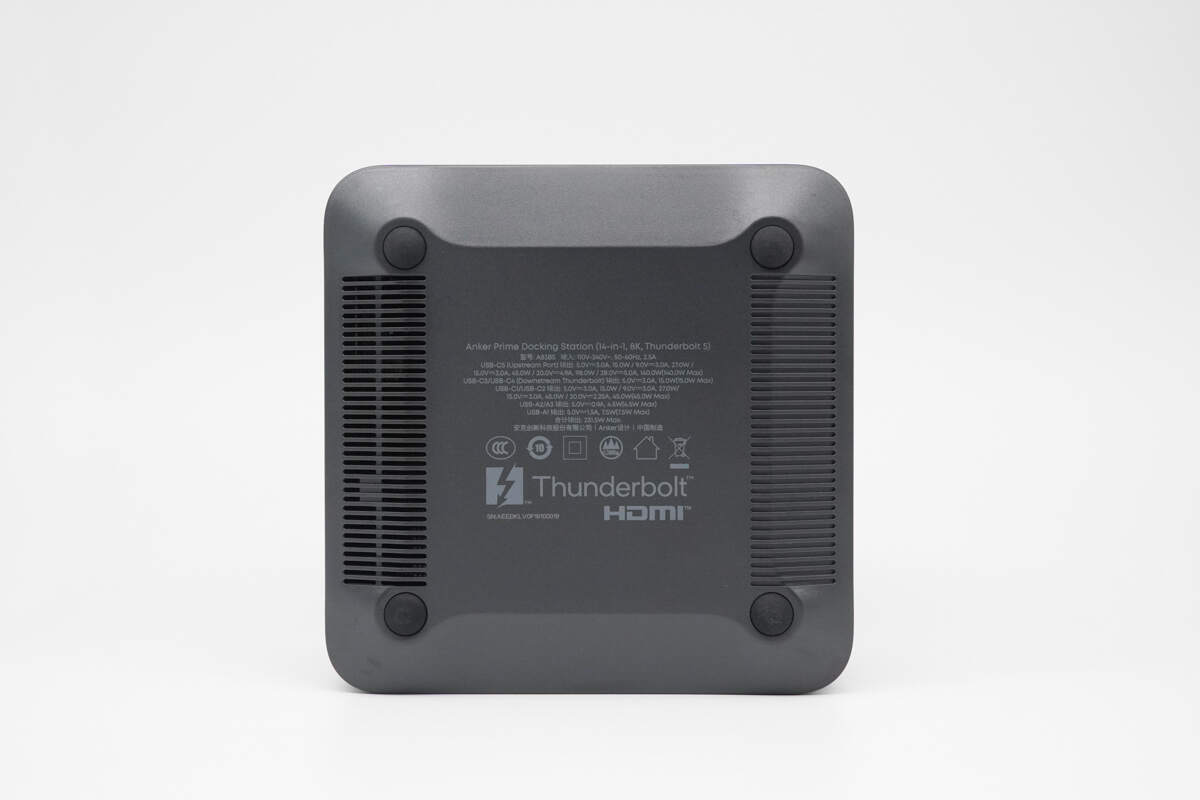
The bottom has non-slip rubber pads. Ventilation openings are located on both sides, and spec info is printed in the center.
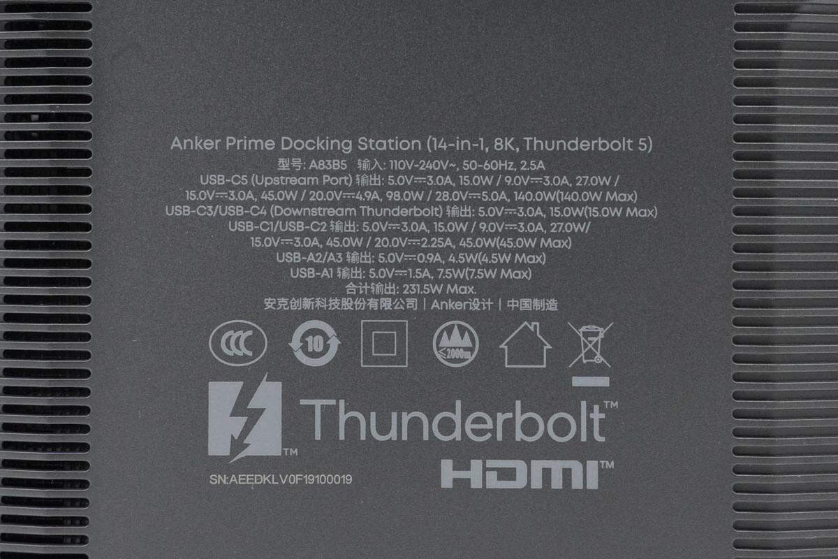
Anker Prime Docking Station (14-in-1, 8K, Thunderbolt 5)
Model: A83B5
Input: 110–240V~, 50–60Hz, 2.5A
Port Specifications:
- USB-C5 (Upstream Port) Output: 5V⎓3A (15W), 9V⎓3A (27W), 15V⎓3A (45W), 20V⎓4.9A (98W), 28V⎓5A (140W)(Up to 140W Max)
- USB-C3 / USB-C4 (Thunderbolt Downstream Ports) Output: 5V⎓3A (15W Max)
- USB-C1 / USB-C2 Output: 5V⎓3A (15W), 9V⎓3A (27W), 15V⎓3A (45W), 20V⎓2.25A (45W)(Up to 45W Max)
- USB-A2 / USB-A3 Output: 5V⎓0.9A (4.5W Max)
- USB-A1 Output: 5V⎓1.5A (7.5W Max)
Total Combined Output: 231.5W Max
Designed by Anker Innovations Co., Ltd.
Designed by Anker – Made in China
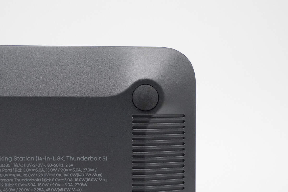
Close-up of the bottom non-slip rubber pads.
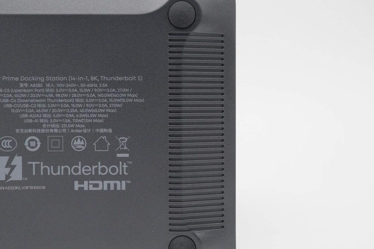
Close-up of the ventilation openings.
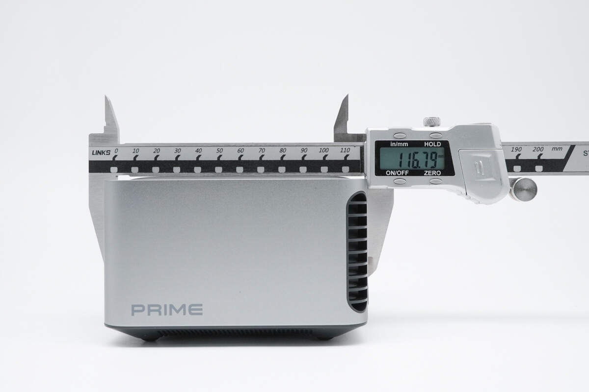
The length of the dock is about 116.8 mm (4.6 inches).
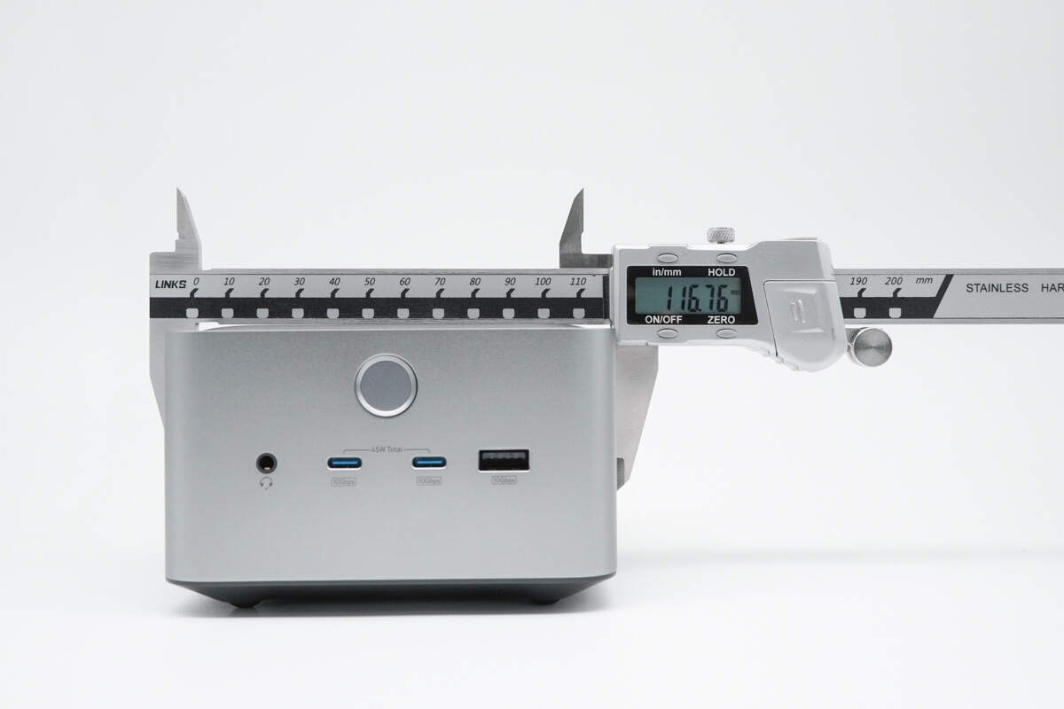
The width is about 116.8 mm (4.6 inches).
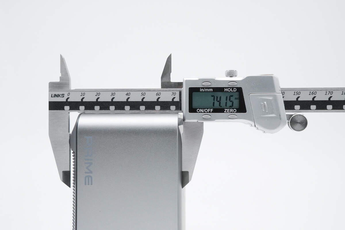
The height is about 74.2 mm (2.92 inches).
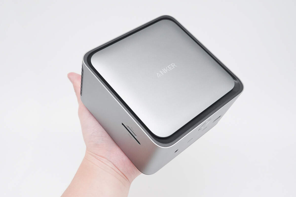
That's how big it is in the hand.
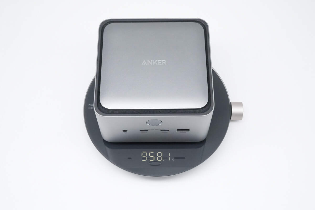
The weight is about 958 g (33.79 oz).
Connect the docking station to a power source.
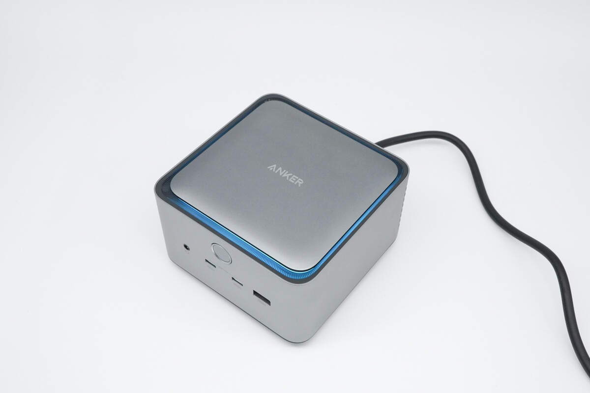
The ambient light on the top of the device turns on, indicating that the dock is powered.
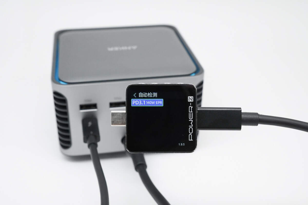
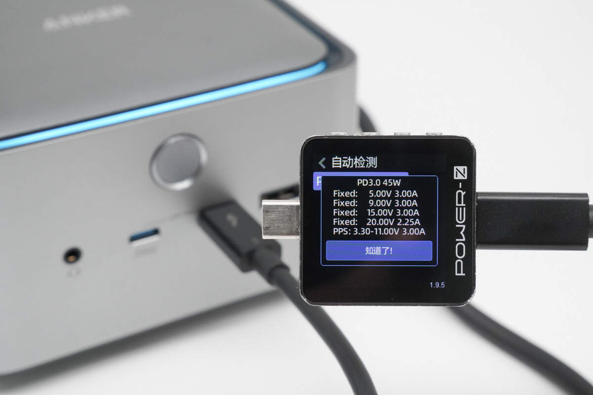
ChargerLAB POWER-Z KM003C shows that the USB-C5 supports PD3.1 140W charging protocol.
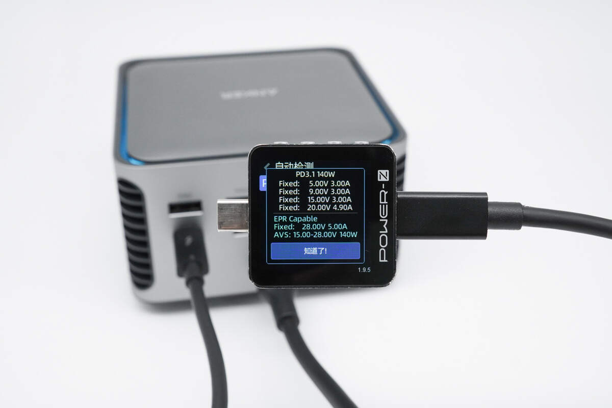
It supports five fixed PDOs of 5V3A, 9V3A, 15V3A, 20V4.9A, and 28V5A. It also has a set of AVS, which is 15-28V 140W.
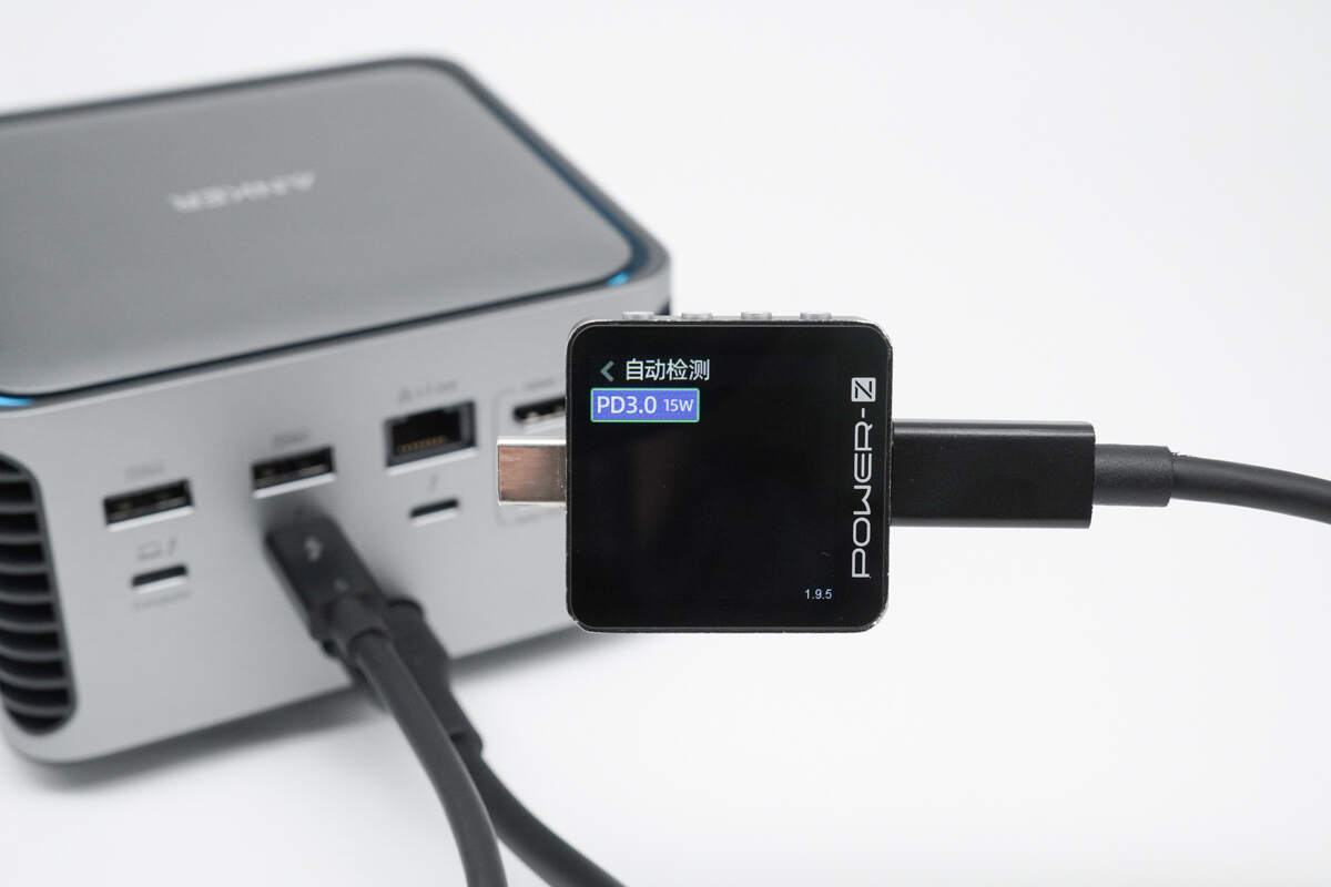
The USB-C3 and USB-C4 ports support the same protocols and support PD 3.0 output at up to 15W.
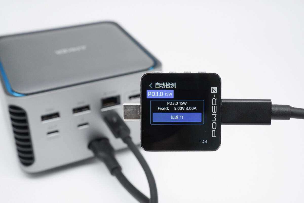
The USB-C3 and USB-C4 ports support a PDO of 5V3A.
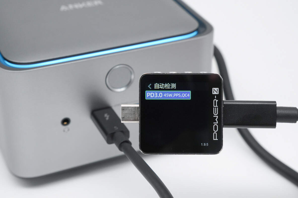
The USB-C1 and USB-C2 ports support the same protocols, including PD 3.0, PPS, and QC4.
They support four fixed PDOs of 5V3A, 9V3A, 15V3A, 20V2.25A, and a set of PPS, which is 3.3-11V3A.
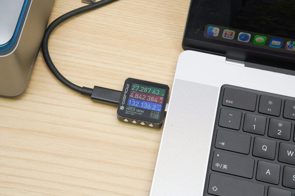
Use it to charge the MacBook Pro 16 M4 Pro, the output voltage is 27.3V, the current is 4.84A, and the charging power is about 132W. This indicates that PD 3.1 fast charging has been successfully activated.
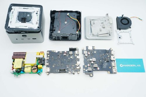
Teardown
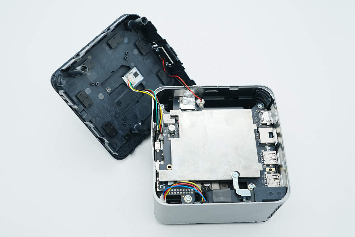
Next, let's take it apart to see its internal components and structure.
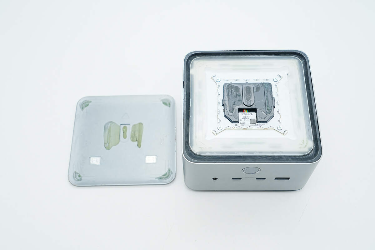
First, pry open the top cover, which is fixed with glue.
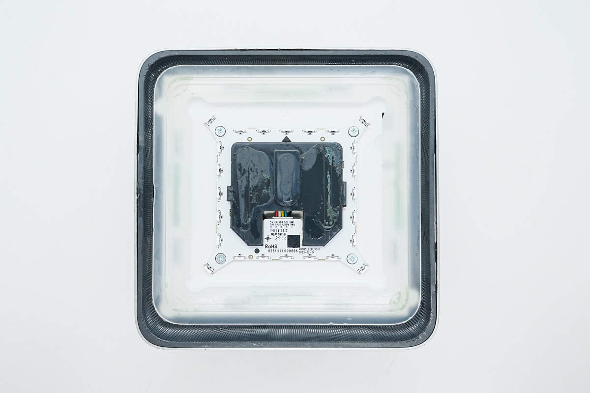
The inside of the cover contains a light diffuser panel and an LED light board.
The LED light board is fixed by screws.
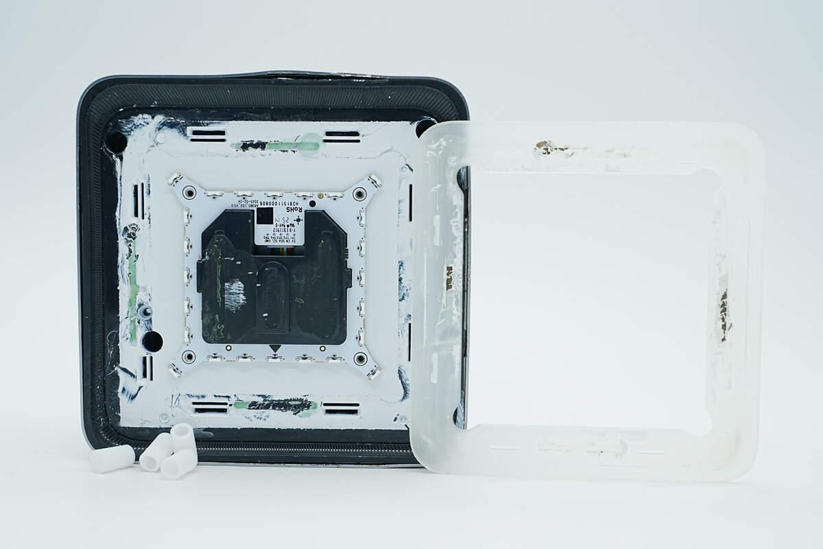
The light diffuser panel is fixed with glue.
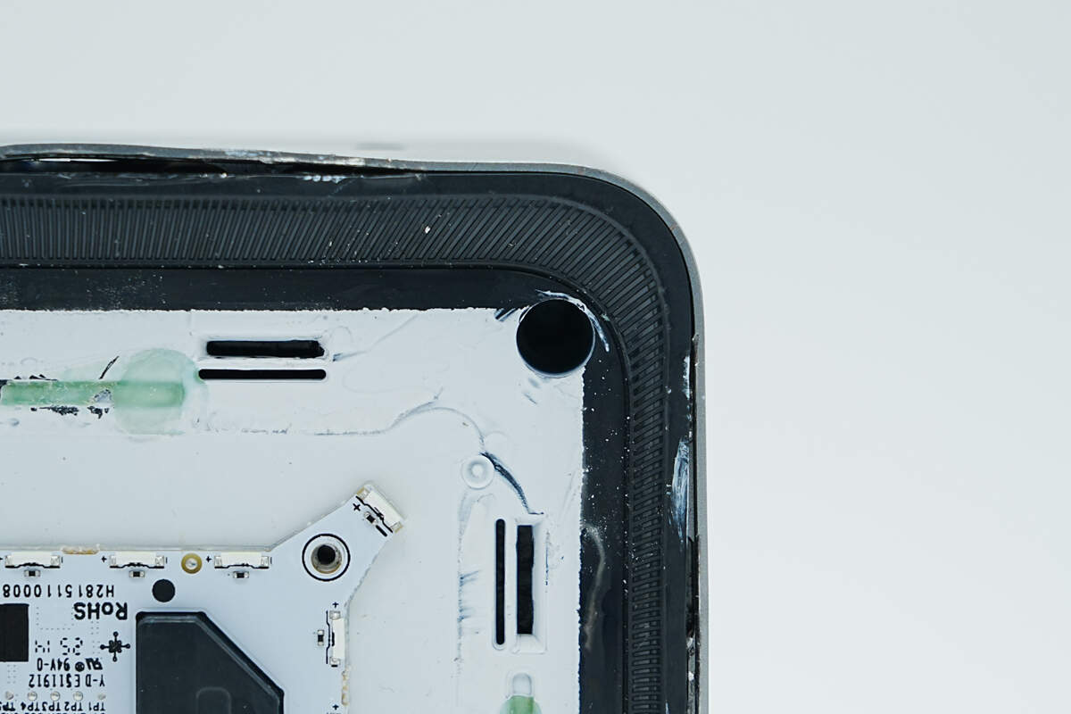
There are fixing screws inside the openings.
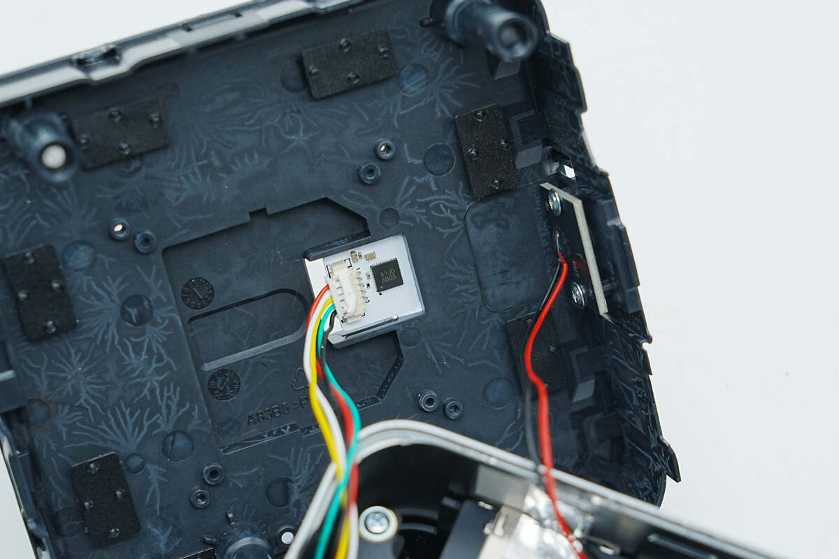
After removing the screws, you can see that the light board and the button are connected by wires.
All the connecting wires are attached using plug-in connectors.
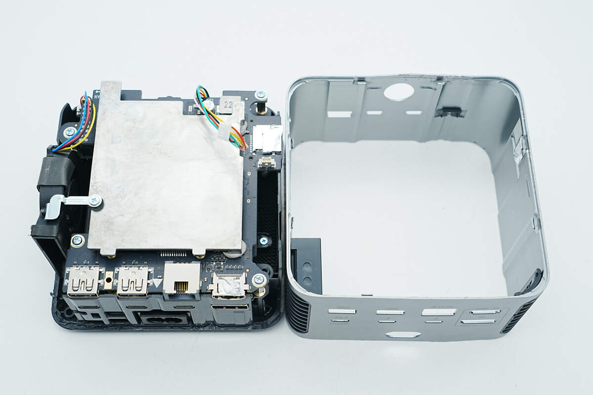
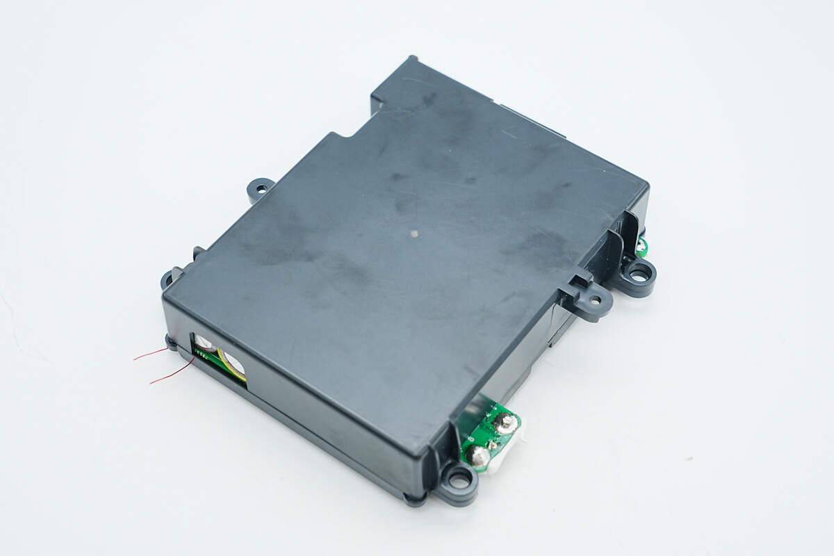
Inside the aluminum alloy enclosure is the module of the dock.
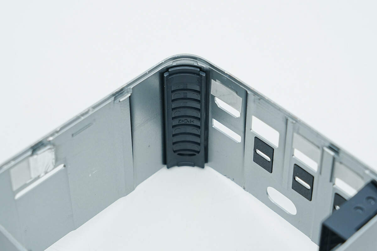
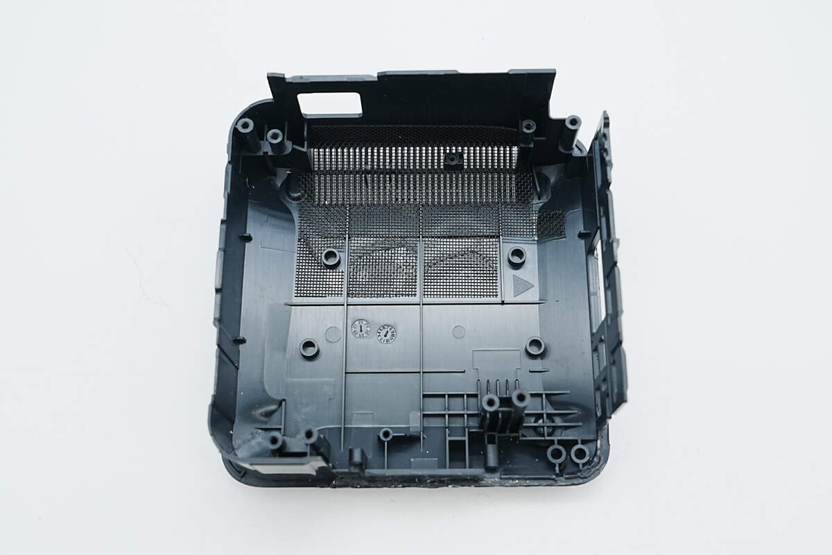
This is the air intake grille on the inside of the enclosure.
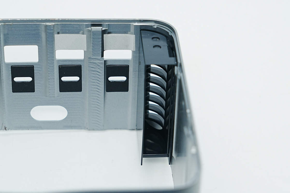
The other side features an exhaust grille.
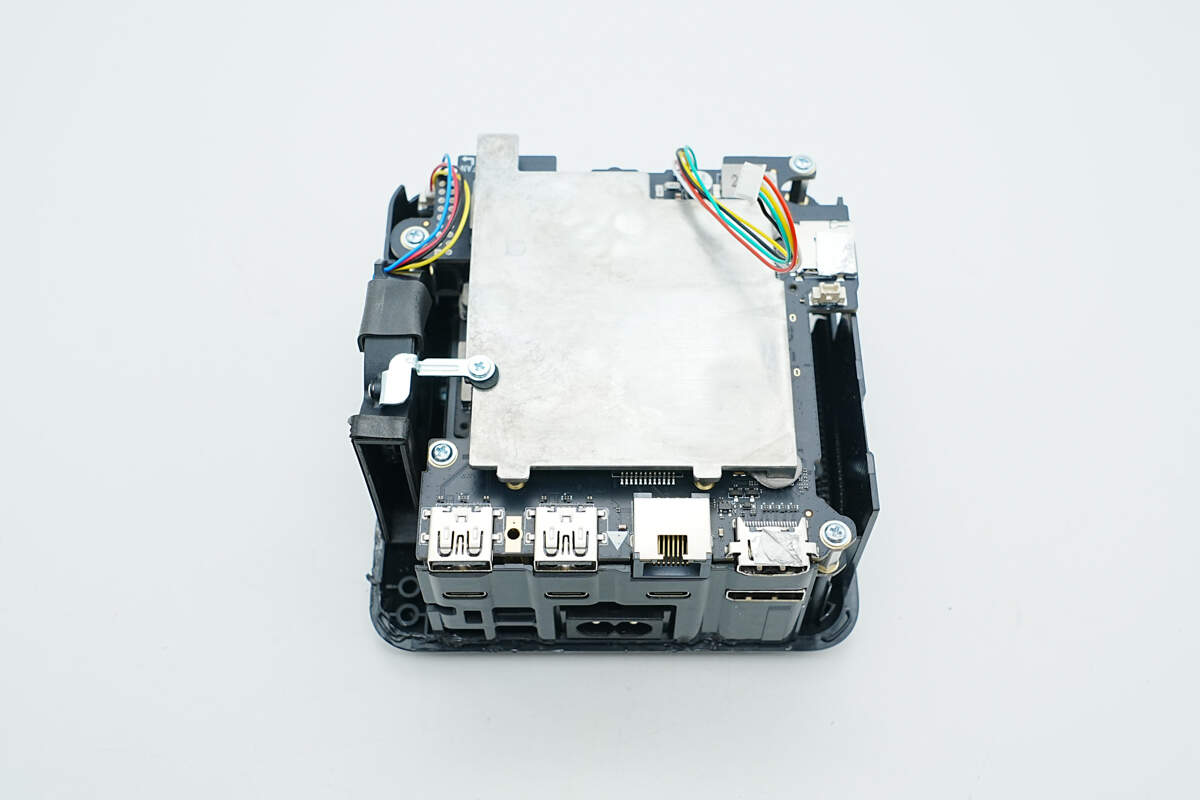
The PCBA module uses a multi-layer stacked design and is secured with screws. An aluminum alloy heatsink is mounted on the top for thermal management.
There are standoffs on the side of the PCBA module for mounting and securing.
The PCBA module is mounted on the plastic frame.
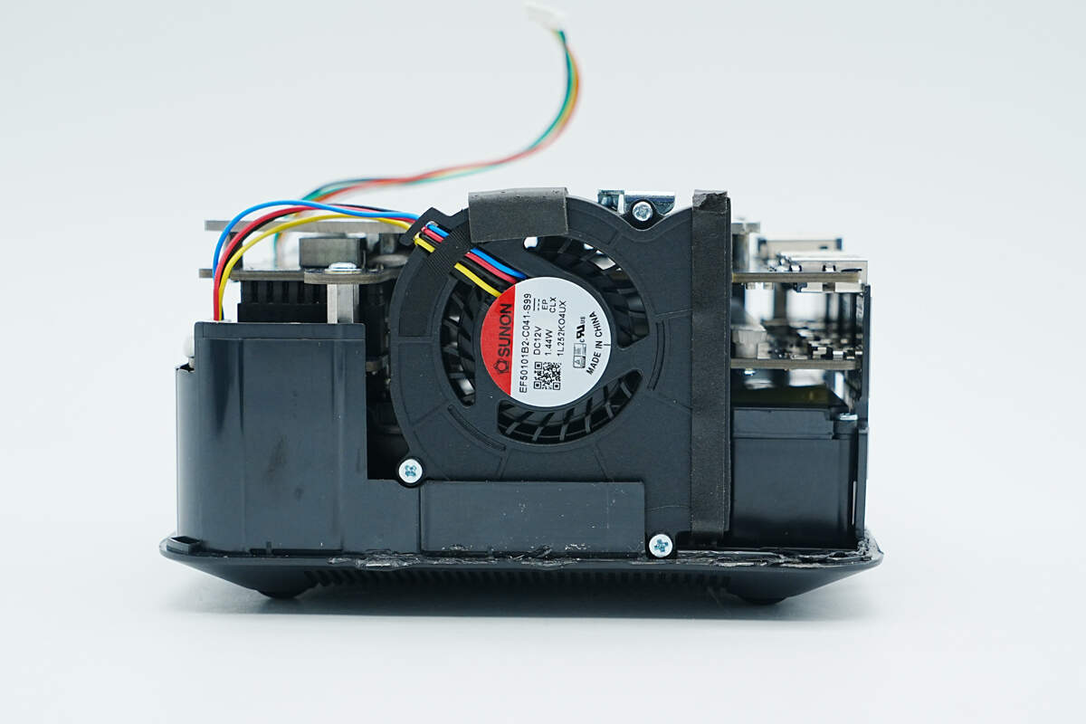
This side features a cooling fan.
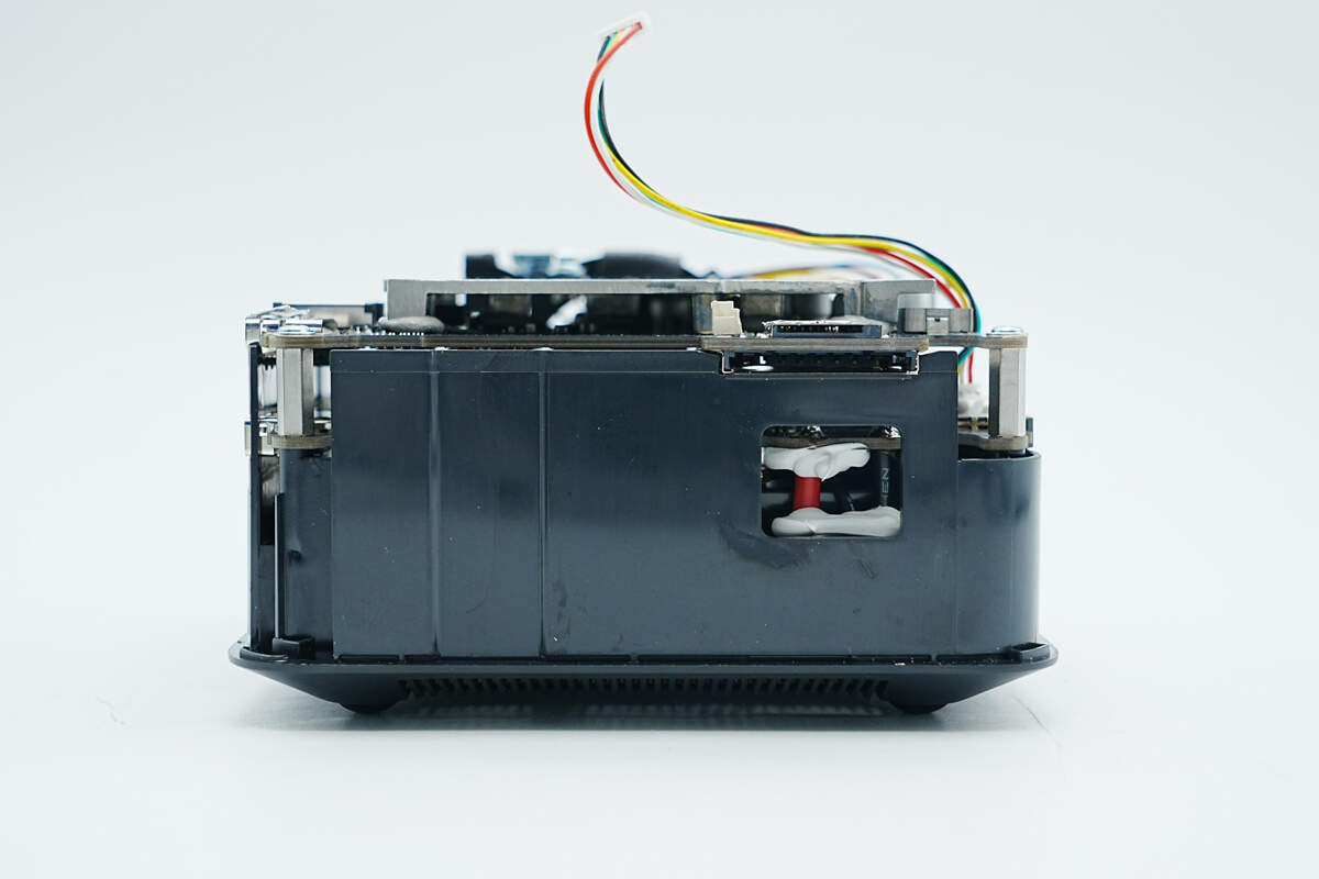
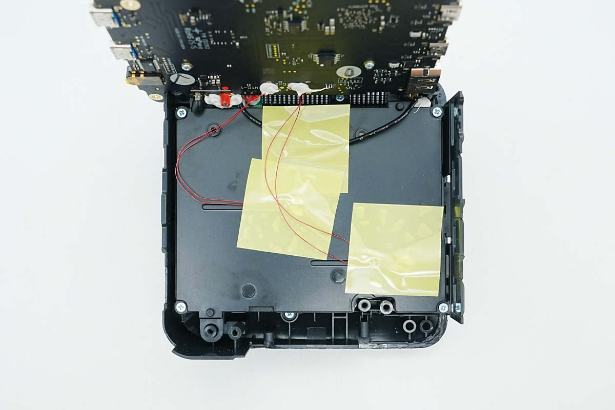
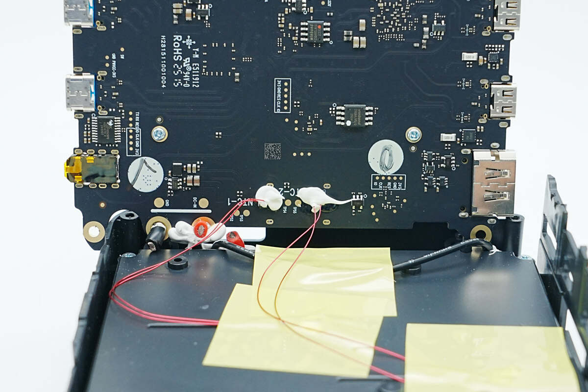
The other side contains the power wires.
The back side features the power input socket and port sockets.
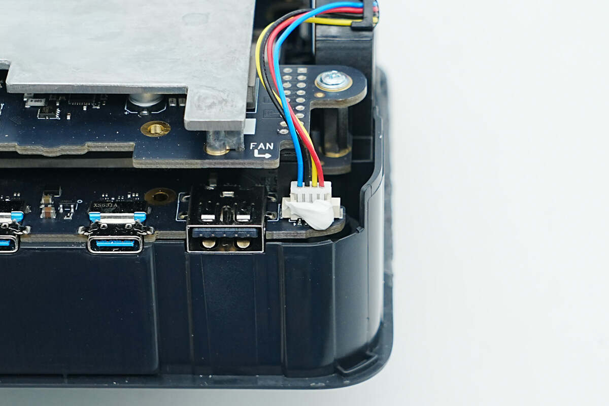
The cooling fan connector is reinforced with glue.
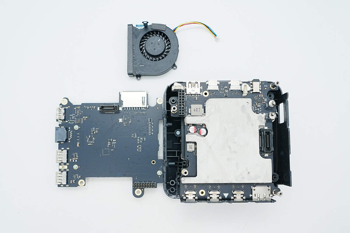
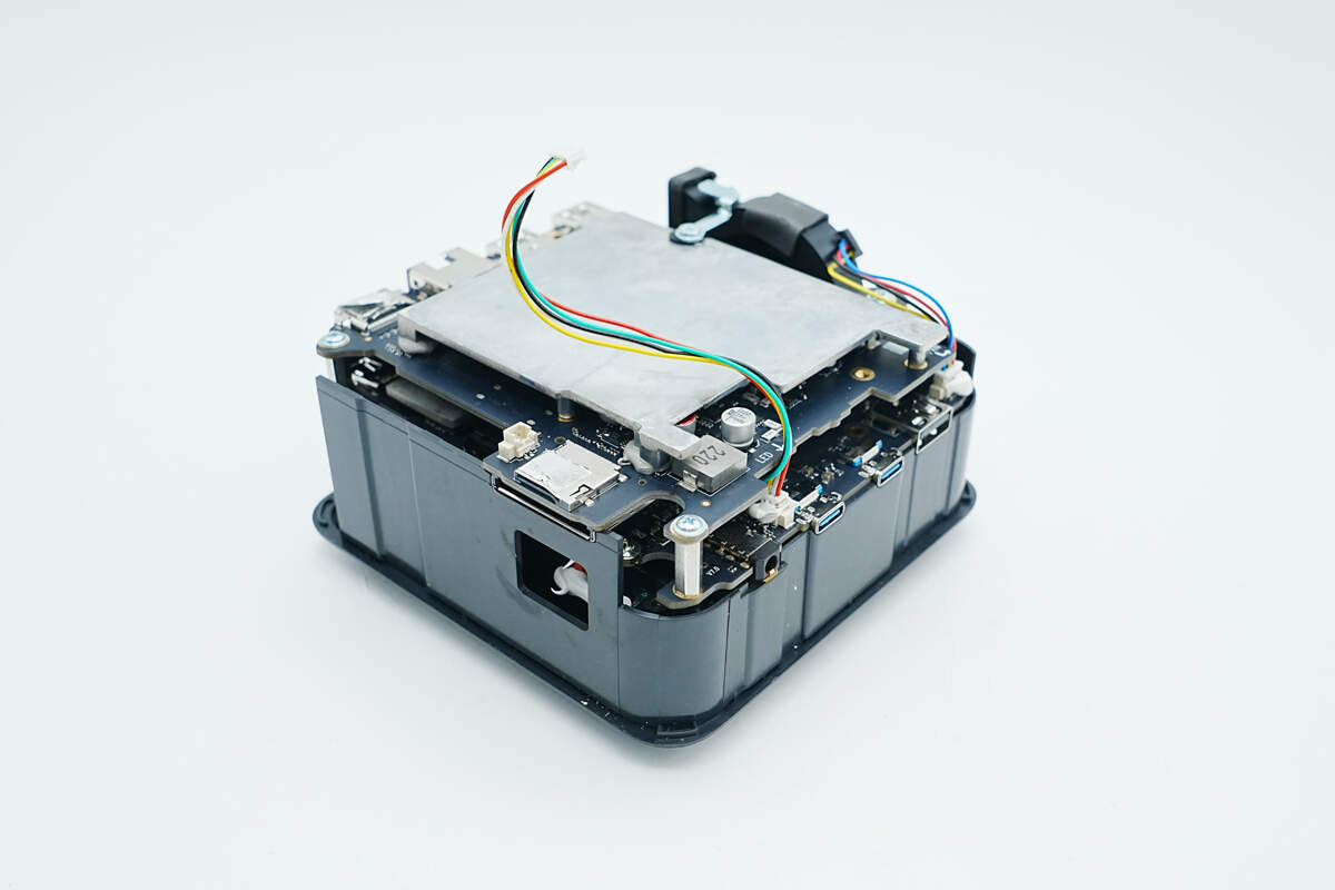
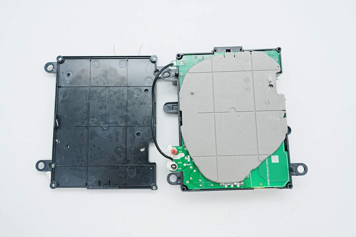
After removing the screws, the upper PCB can be taken off. It is connected via pin headers and connectors. The lower module is also equipped with a heatsink.
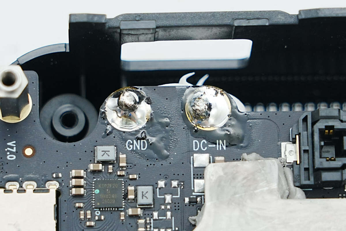
The power wires are connected by soldering.
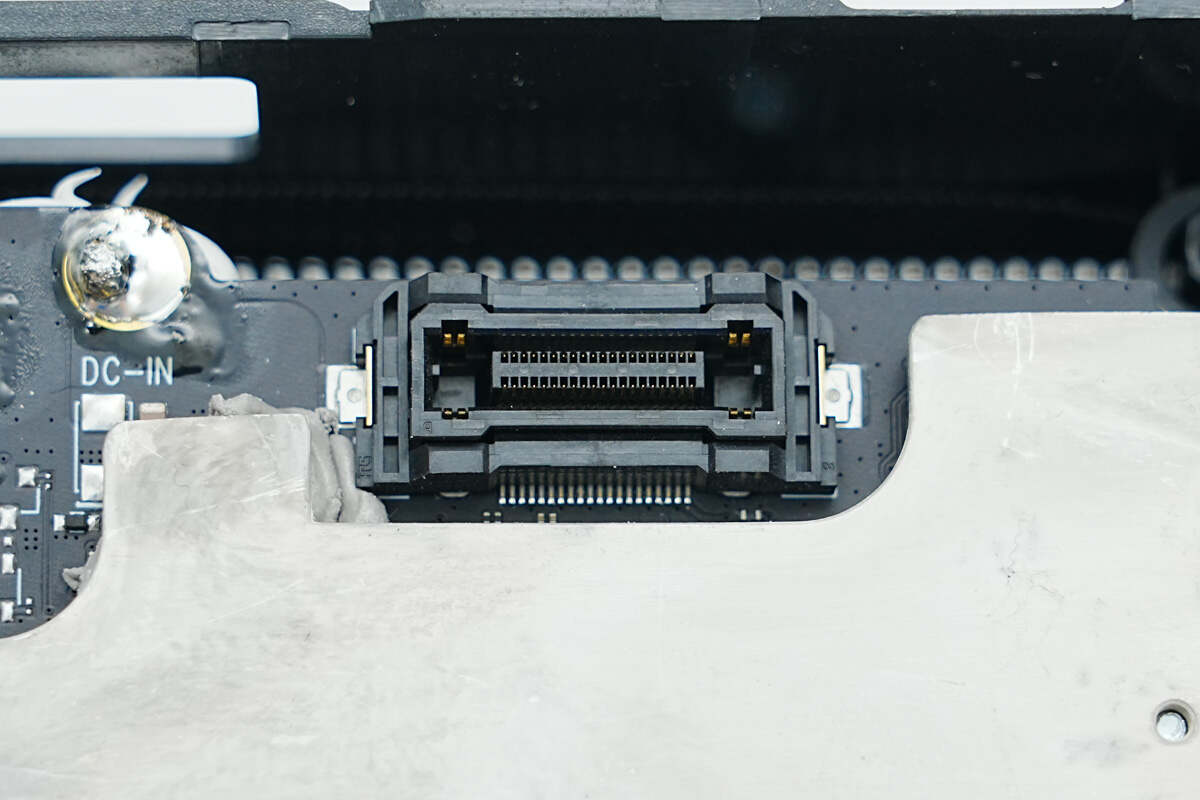
This is the connector that links the upper and lower PCBs.
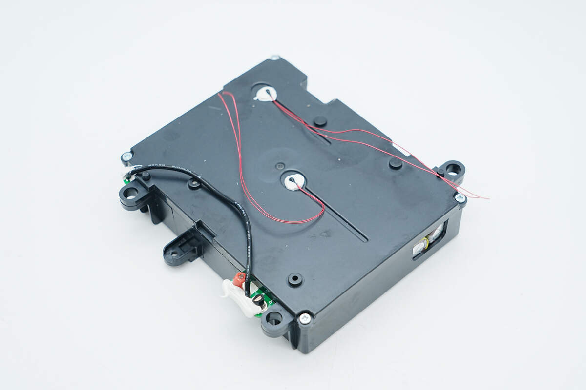
The power module is located at the bottom. The thermistors are held in place with tape.
The thermistors are soldered to the PCBA module.
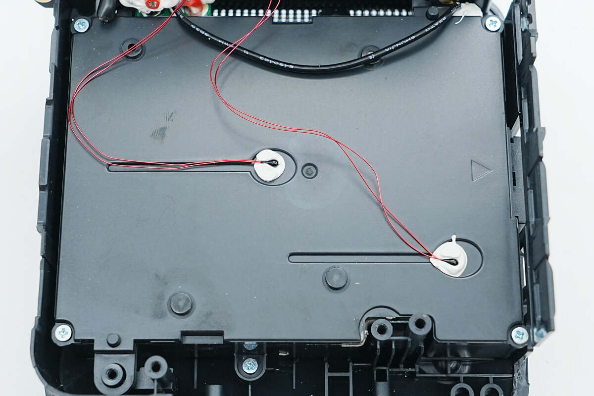
Remove the tape, and you will see that the two thermistors are reinforced with glue.
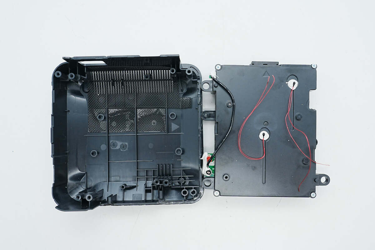
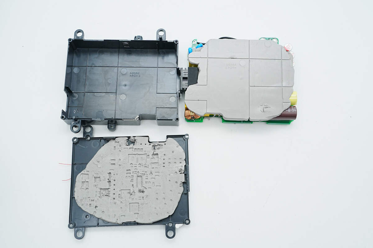
Remove the power module.
The lower casing features an air intake grille with a dust filter installed inside.
The power module casing is secured with screws.
Mounting holes are provided on the side of the power module housing.
After unscrewing the screws and opening the casing, potting compound is found filling the gap between the power module and the casing.
Potting compound is applied to both sides of the casing to enhance heat dissipation.
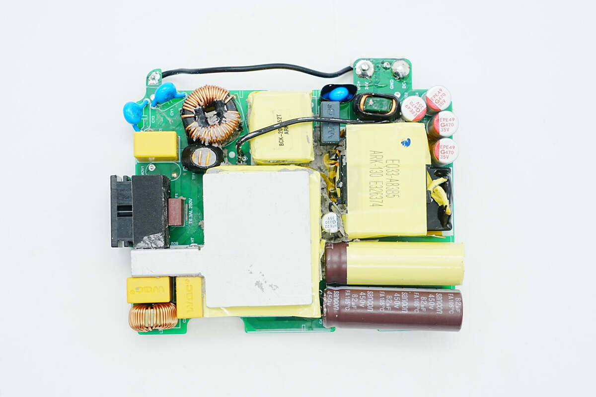
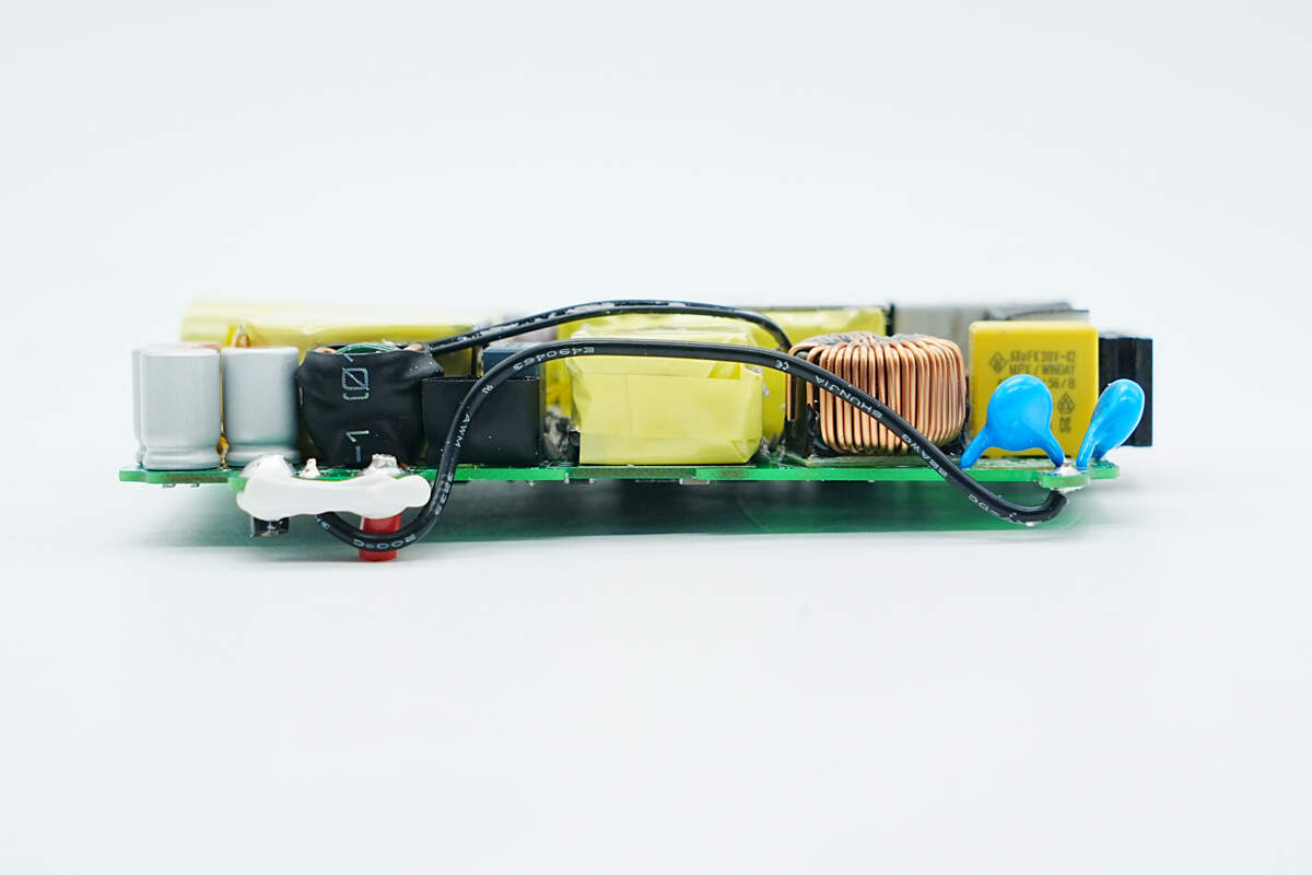
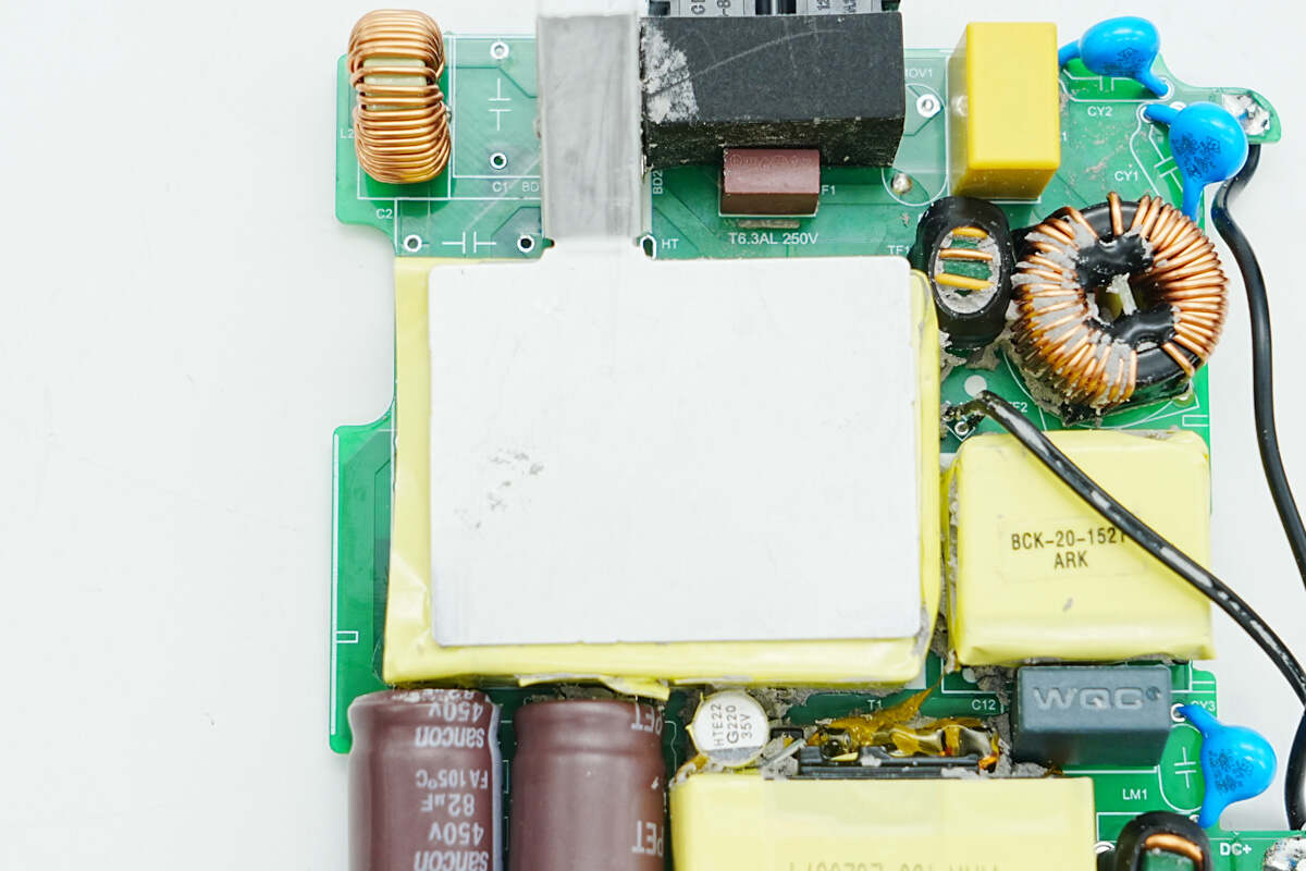
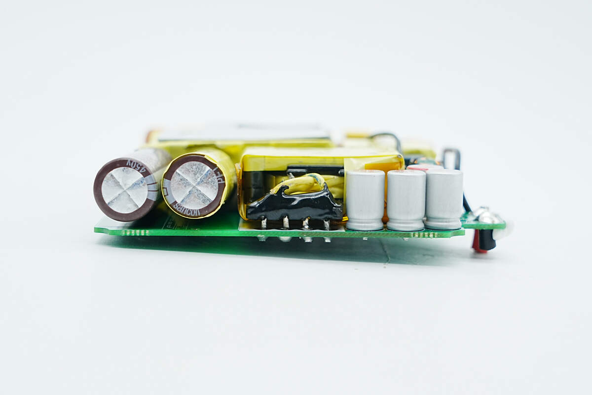
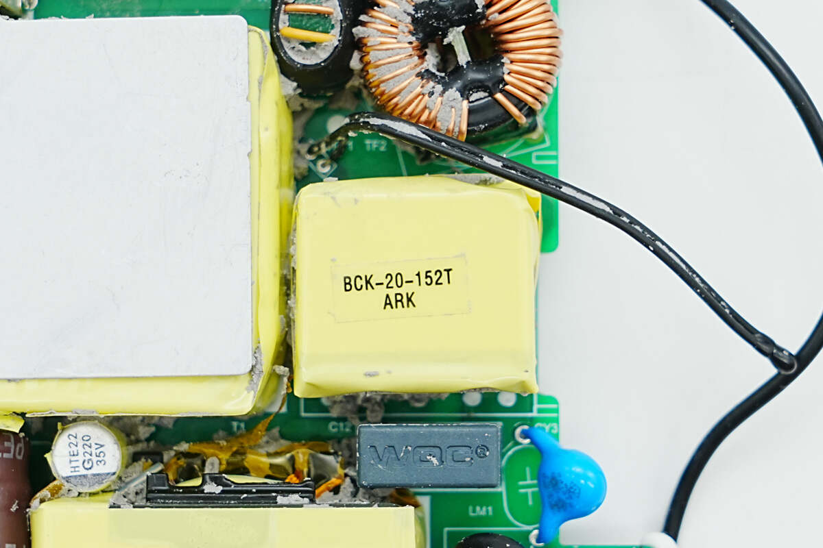
After removing the potting compound, a power socket and fuse are located in the middle of the left side of the front panel. Above them are a safety X2 capacitor and two common mode chokes, while below are a bridge rectifier, two film capacitors, and a toroidal inductor. The bridge rectifier is fitted with a large heat sink that extends over the PFC inductor.
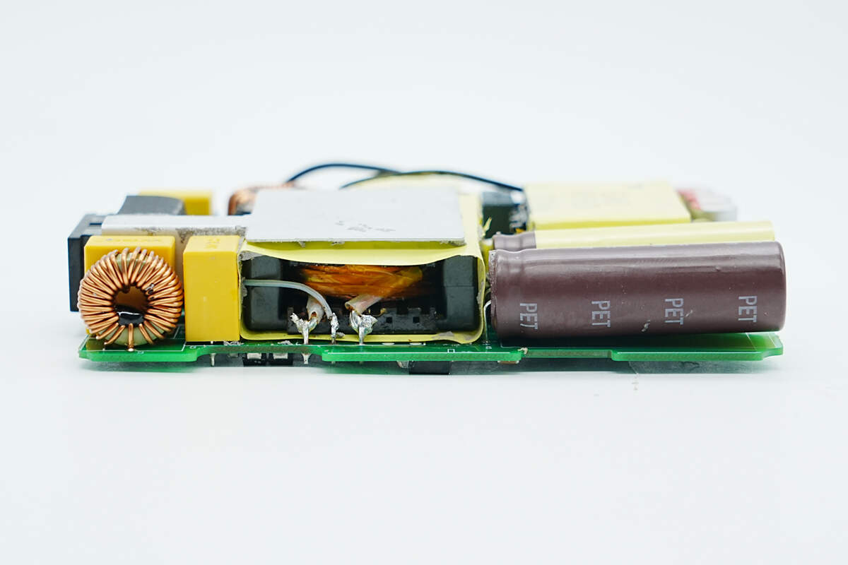
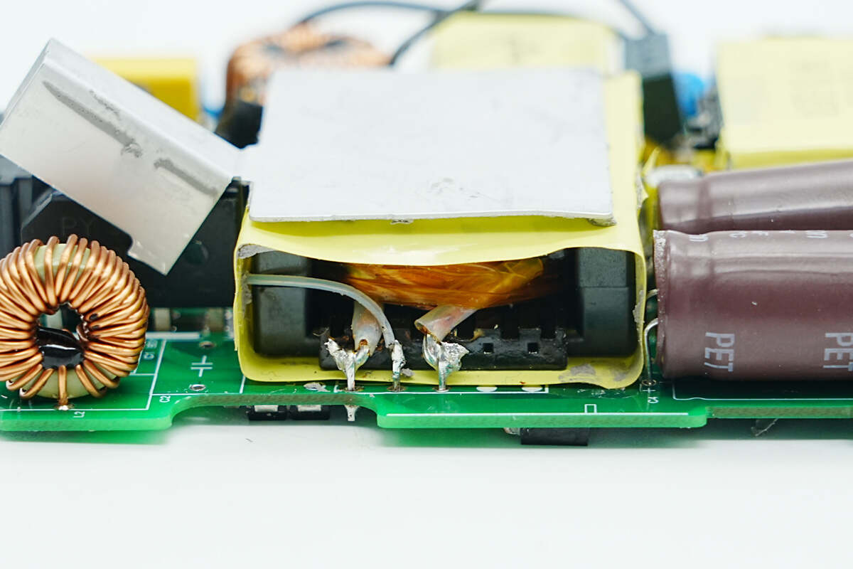
In the lower right corner, there are electrolytic capacitors. Above them are an LLC transformer, a resonant capacitor, a resonant inductor, solid capacitors, and a filter inductor. A thermistor is also placed near the transformer.
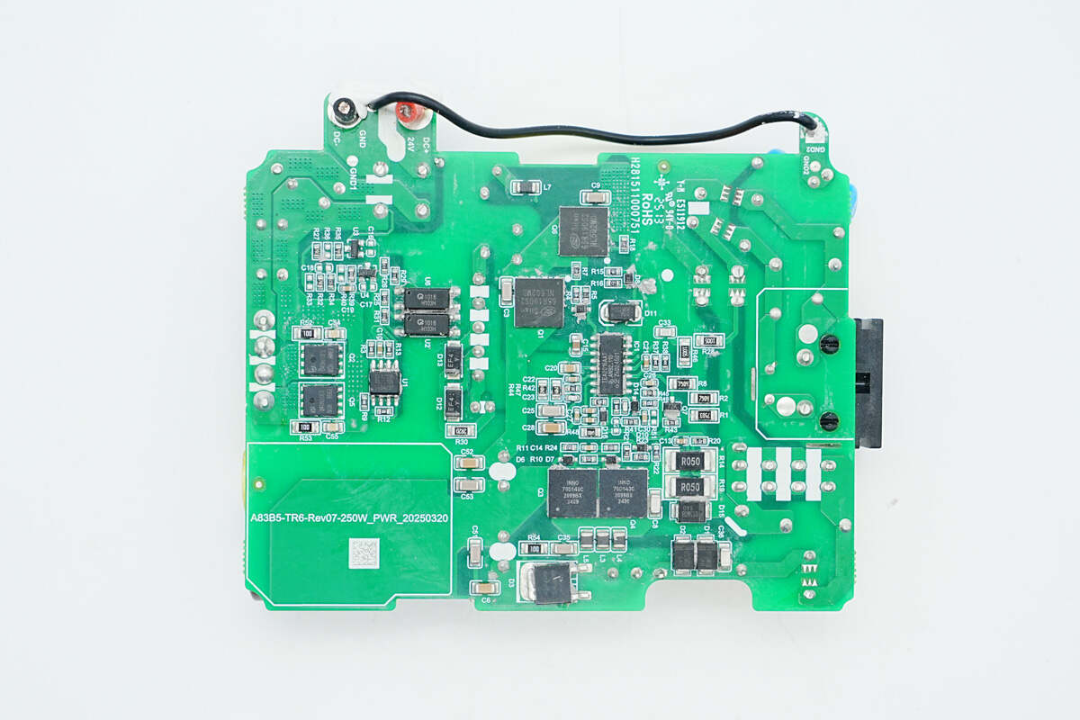
On the back side, there is a PFC + LLC combo controller. Below it are a PFC MOSFET and a PFC rectifier, while an LLC MOSFET is located above.
To the left are a synchronous rectifier controller and a synchronous rectifier. Two optocouplers are placed between the primary and secondary sides for voltage feedback and protection functions.
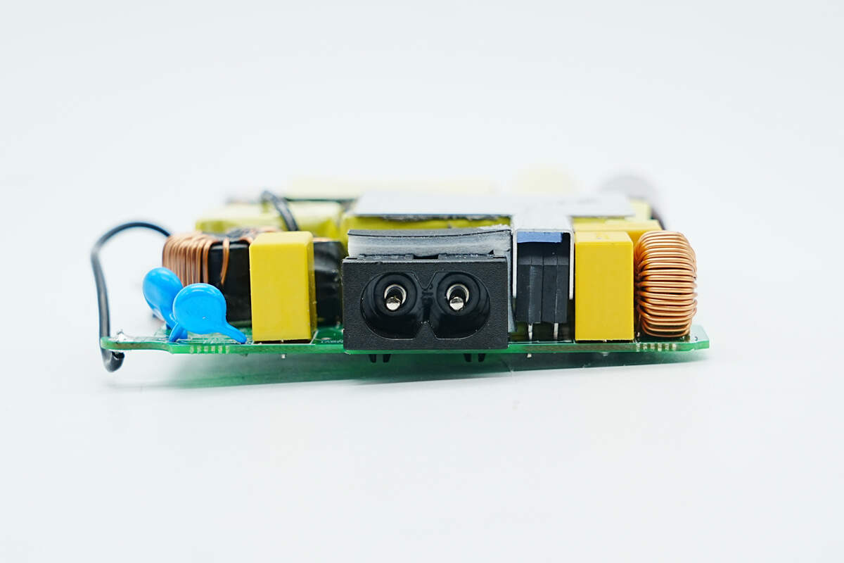
There is the input socket.
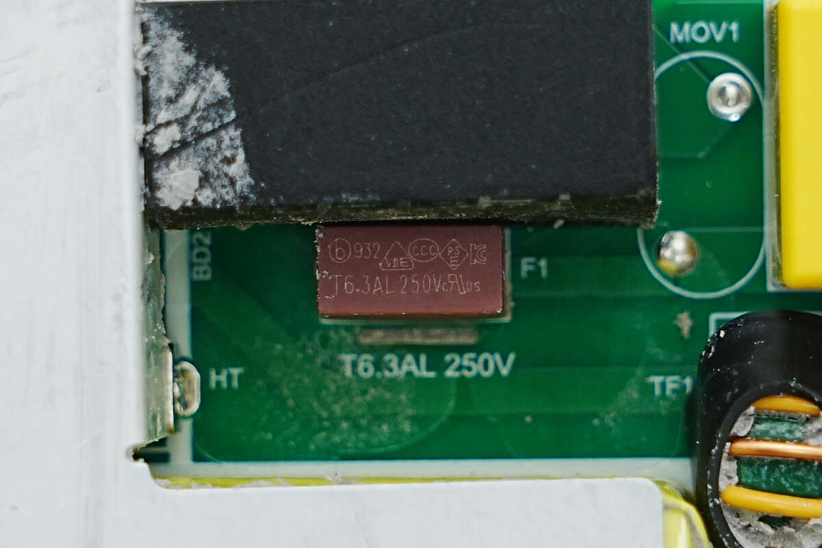
The fuse is from Betterfuse. 6.3A 250V.
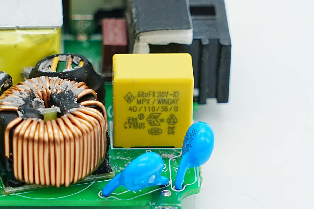
The Safety X2 capacitor is from WINDAY. 0.68μF.
The side of the PCBA module has a capacitor for output filtering, a filter inductor, a Y capacitor, a resonant inductor, and a common mode choke."
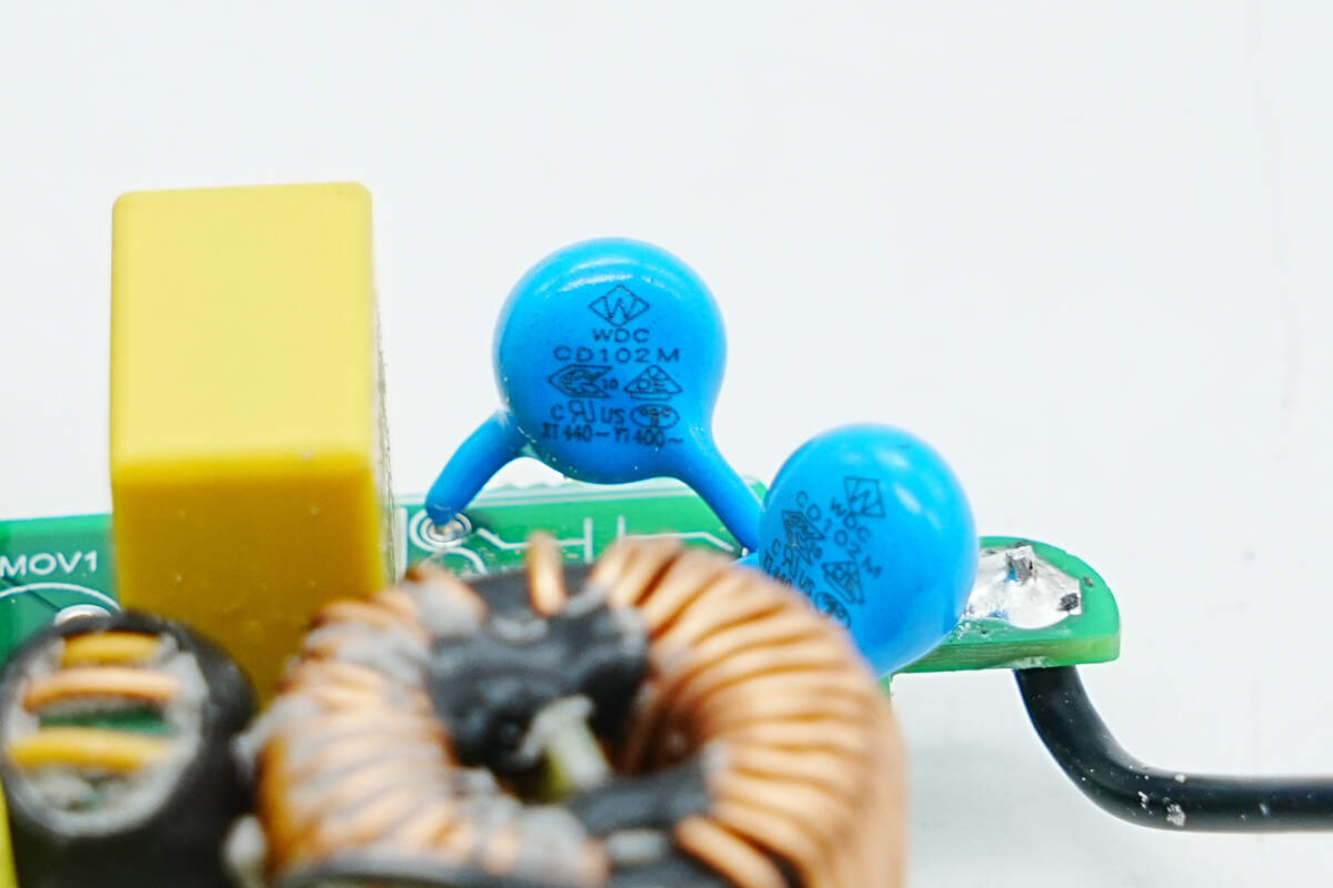
The Blue Y capacitor is from WINDAY. 1000pF.
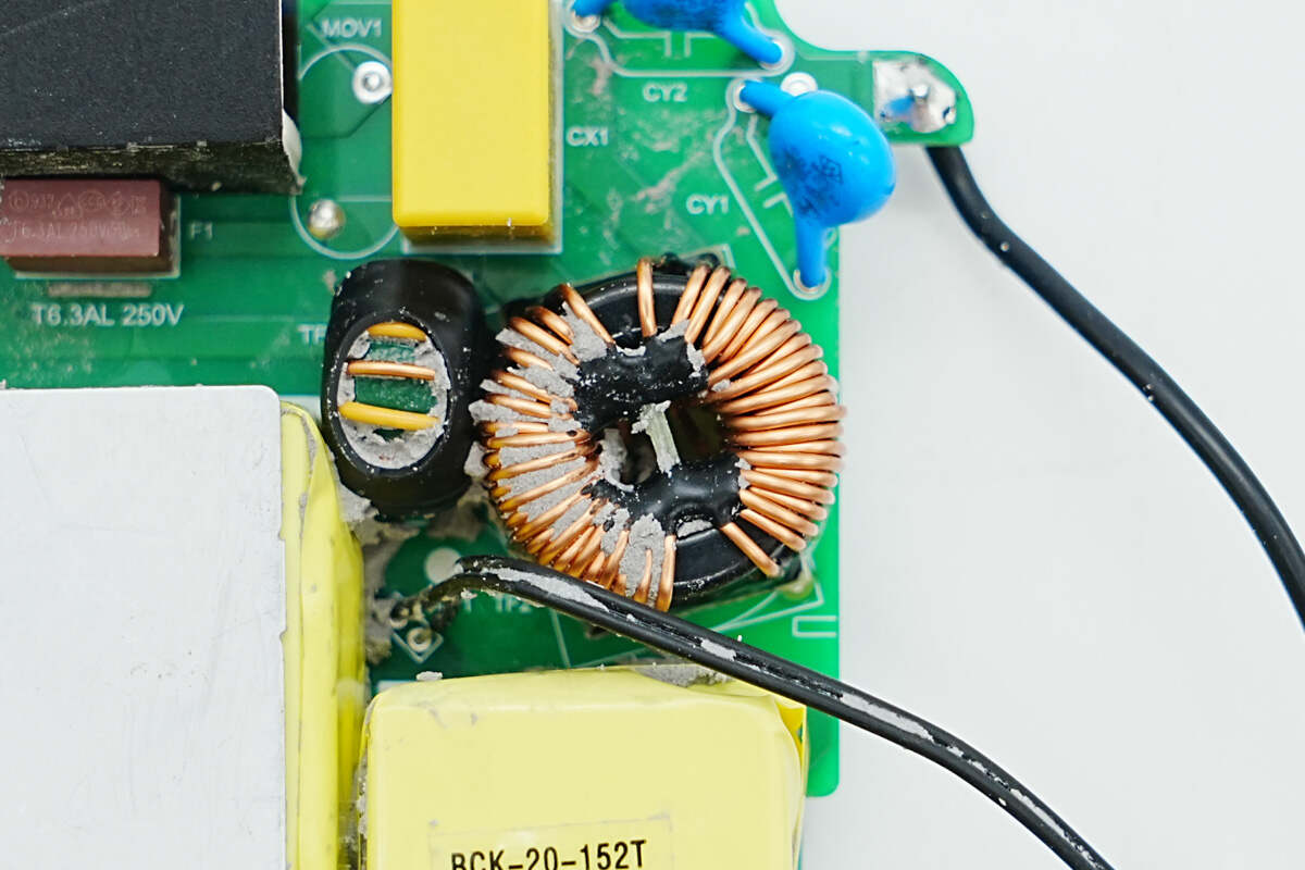
The common mode choke is wound with magnet and insulated wires, and it's also insulated with bakelite.
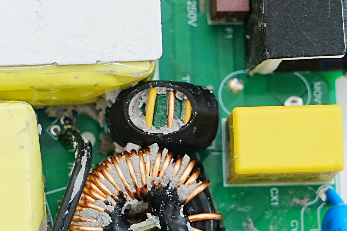
The other common mode choke is also wound with magnet and insulated wires, and it's also insulated with bakelite.
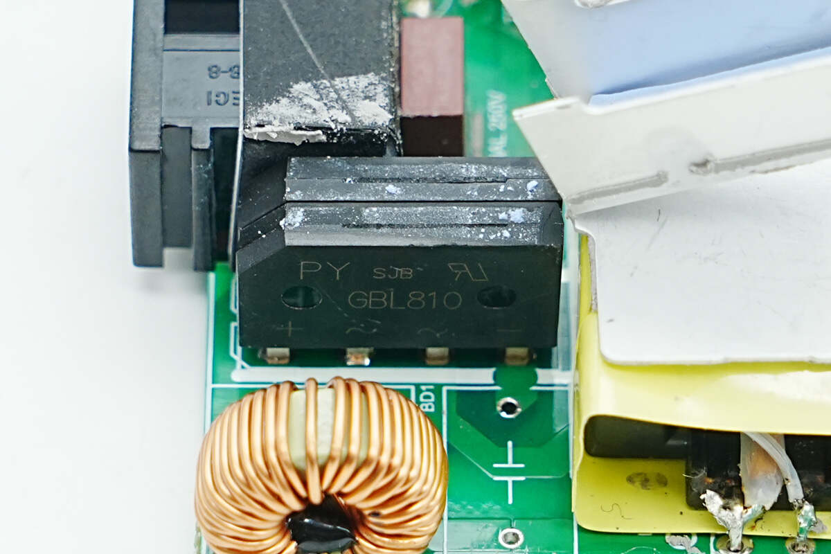
Remove the heat sink above the bridge rectifier. The bridge rectifier is from Pingwei and adopts the GBL package. The two are connected in parallel to evenly share the heat dissipation. 8A 1000V. Model is GBL810.
This side of the PCBA module has a filter inductor, two film capacitors, a PFC boost inductor, and an electrolytic capacitor."
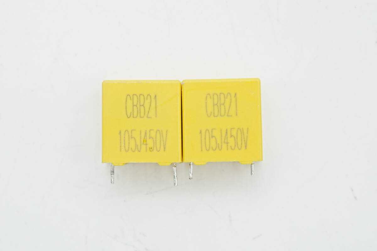
The two film capacitors are from WQC. 1μF 450V.
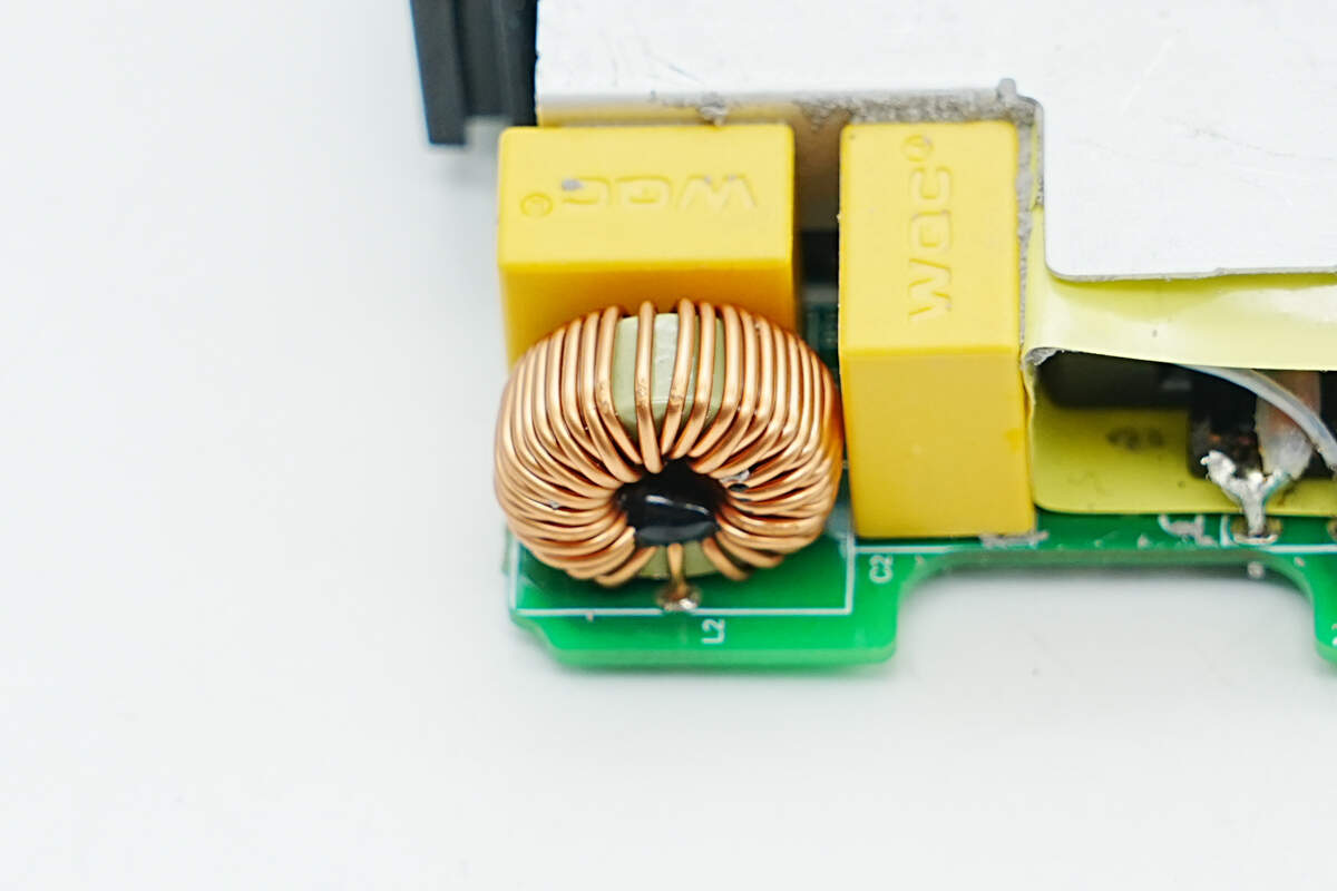
The filter inductor is wound with a magnetic ring.
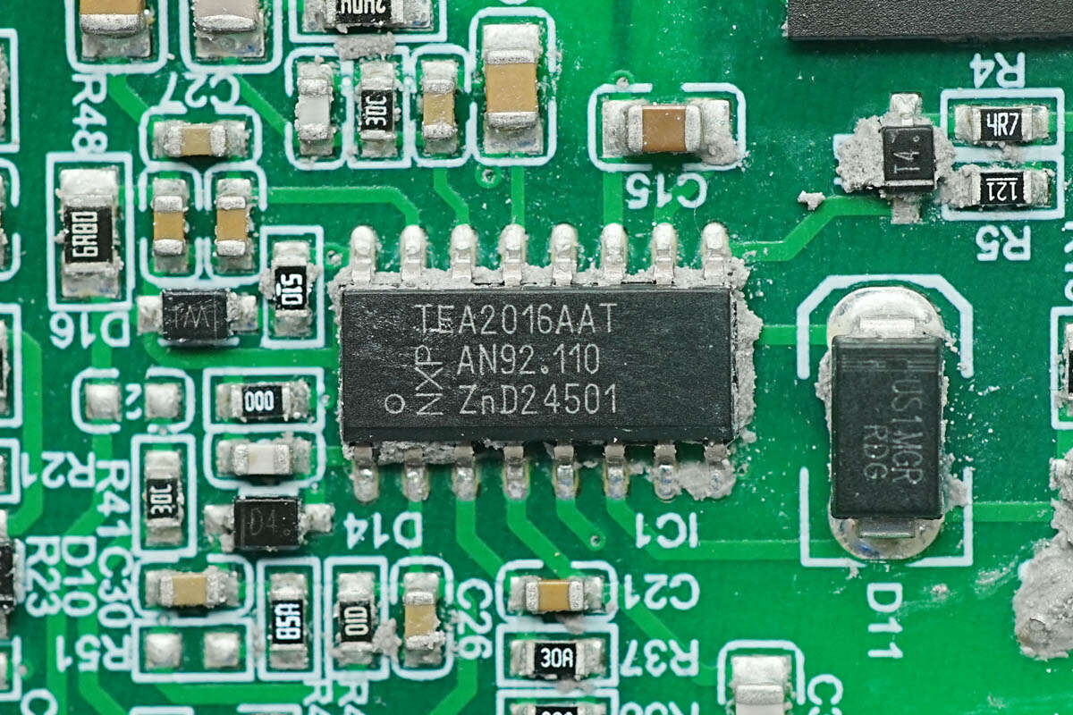
The power supply master control chip is from NXP and adopts the SO16 package. It is a PFC + LLC dual-function controller that uses a digital architecture internally. This simplifies the design while reducing the number of external components, and it integrates multiple comprehensive protection features. Model is TEA2016
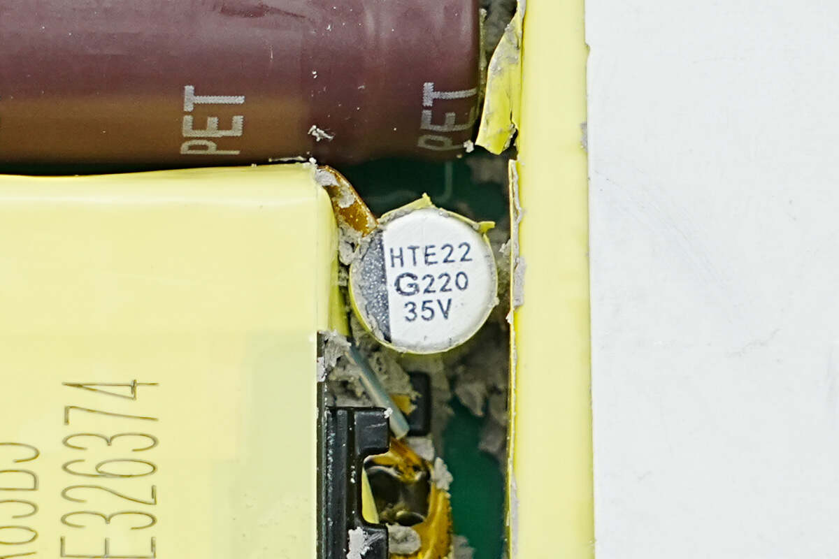
The capacitor supplying power to the master control chip is insulated by wrapped tape. 220μF 35V.
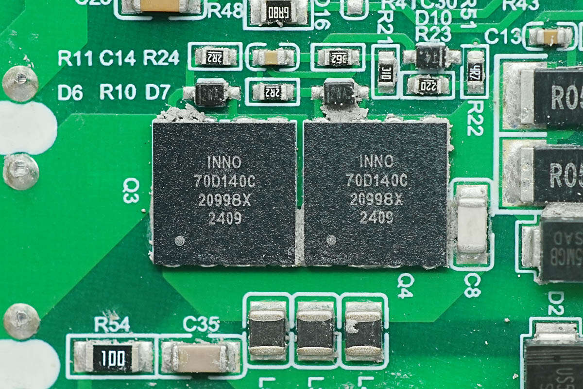
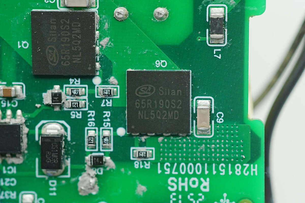
The PFC MOSFET from Innoscience is marked with 70D140C and adopts the DFN8*8 package. It is a 700V-rated enhancement-mode GaN FET with a transient voltage rating of 800V and an on-resistance of 140mΩ. It features a Kelvin source and uses two devices connected in parallel. Model is INN700D140C.
Innoscience GaN FET features extremely low gate charge and output charge, meeting JEDEC standards for industrial applications. It has built-in ESD protection and complies with RoHS, lead-free, and EU REACH regulations. It is suitable for totem-pole PFC, fast charging power supplies, high power density, and high-efficiency switching power supply applications.
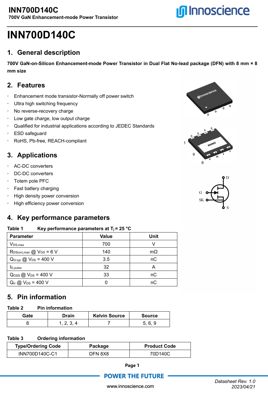
Here is the information about Innoscience INN700D140C.
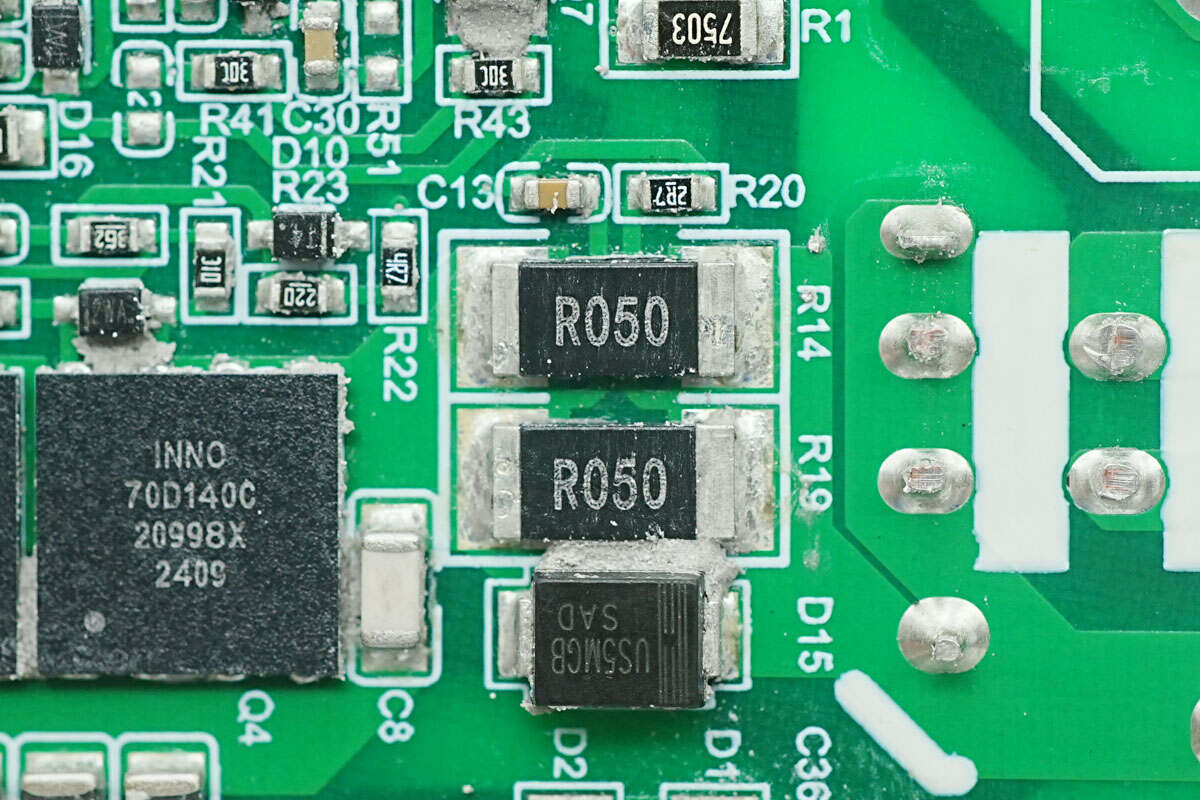
Two 50mΩ resistors are connected in parallel to sense the current of the PFC MOSFET.
A heatsink is attached to the PFC boost inductor.
The PFC boost inductor is wound with Litz wire.
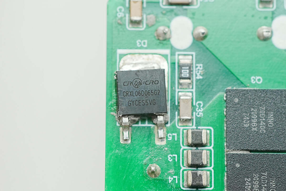
The PFC rectifier is from CR MICRO and adopts the TO-252-2 package. It is a SiC diode. 650V 6A. Model is CRXL06D065G2.
The electrolytic capacitor is insulated with tape.
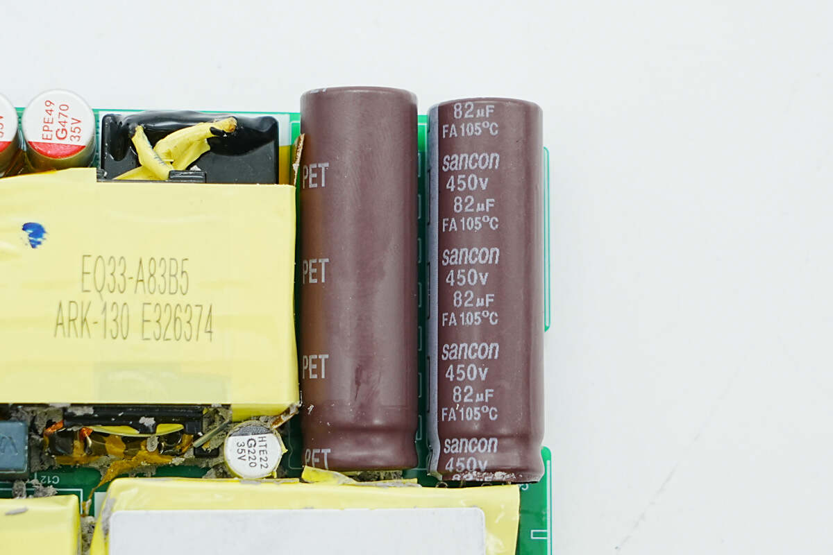
The electrolytic capacitor is from Sancon, specifically the FA series, designed for GaN applications. The specifications are 450V, 82μF. Two identical capacitors are connected in parallel.
The LLC MOSFET is from Silan and adopts the DFN-4-8*8*0.85-2.0 package. 650V 155mΩ. Model is STS65R190L8AS2TR.
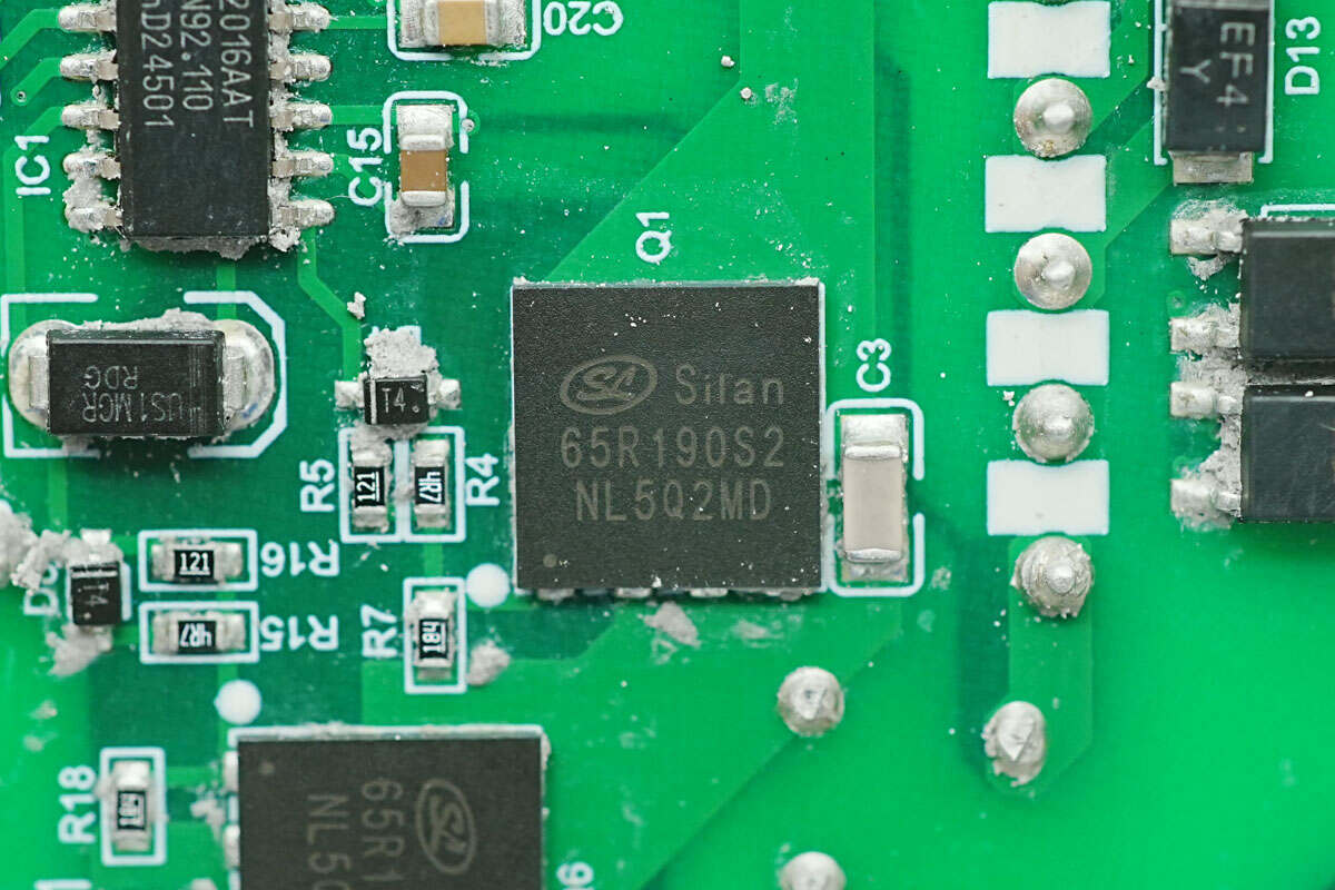
The other MOSFET is of the same model.
The resonant inductor is insulated by tape.
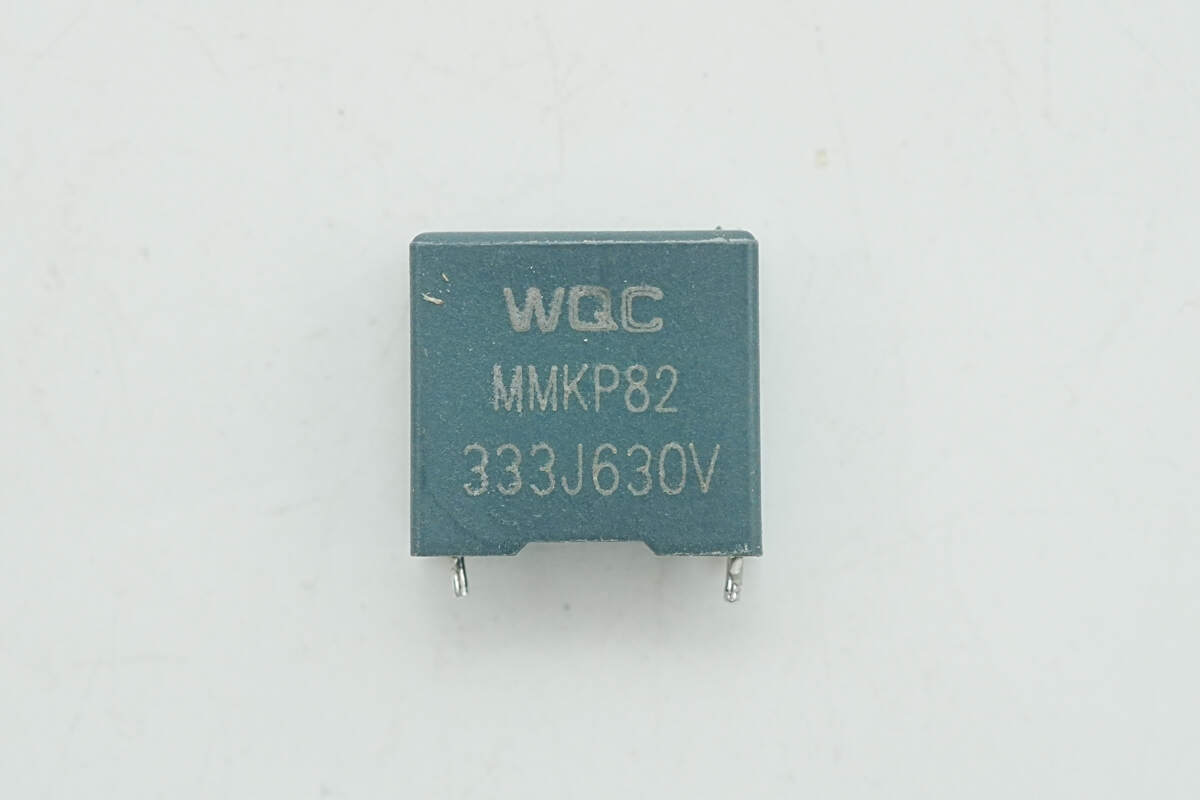
The resonant capacitor is from WQC. 0.033μF 630V.
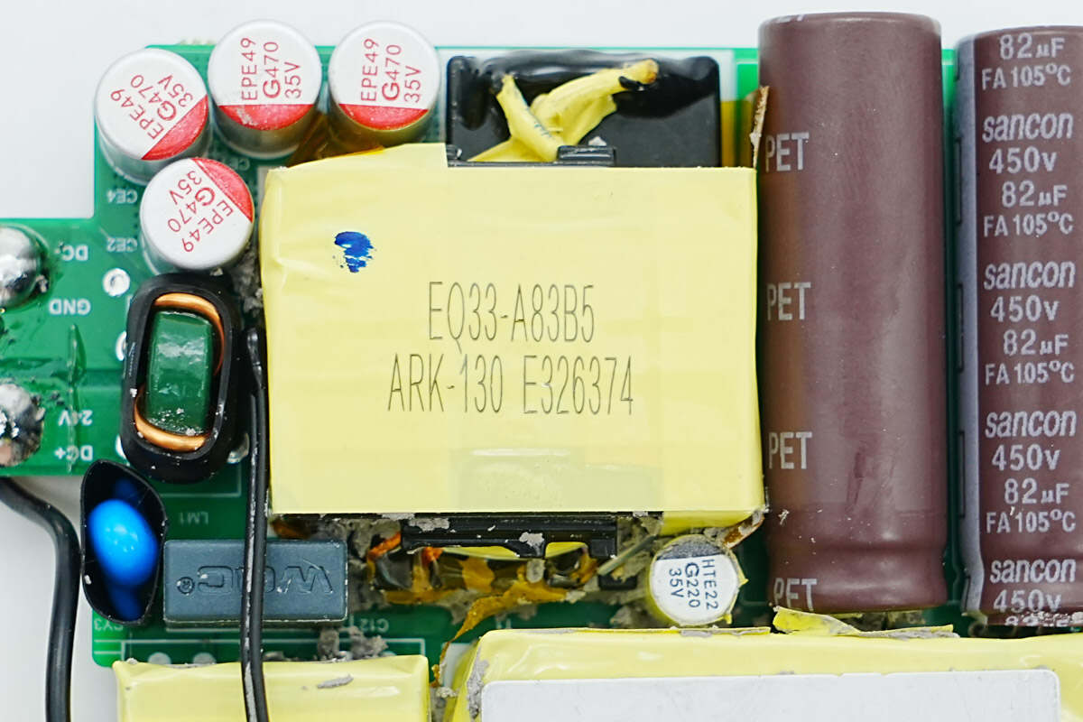
The LLC transformer uses an EQ33 core.
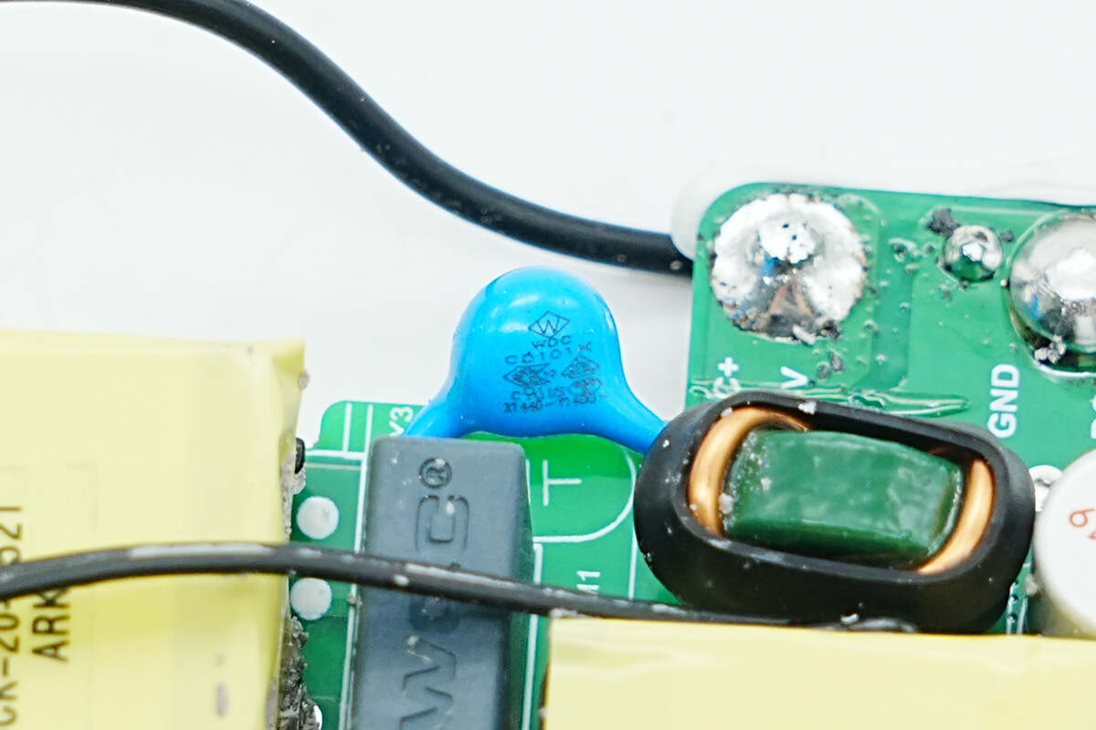
The blue Y capacitor is from WINDAY. 1000pF.
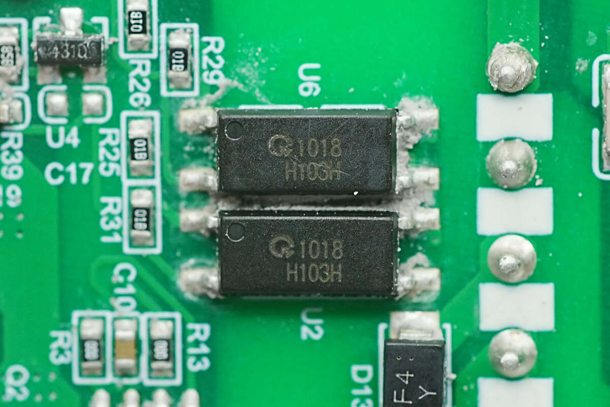
The two feedback optocouplers are from Qunxin Microelectronics and adopt the LSOP4 package. Model is QX1018.

The synchronous rectifier controller is from NXP and adopts the SO8 package. It is a dual-channel synchronous rectifier controller with two integrated drivers, capable of driving two synchronous rectifiers simultaneously or operating independently. It is suitable for use in LLC resonant power supplies. Model is TEA2095.
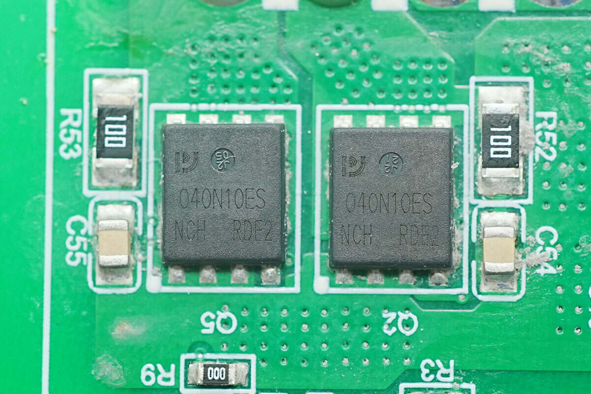
The synchronous rectifier is from Pingwei and adopts the DFN5*6 package. 100V 3.4mΩ. Model is PW040N10ES.
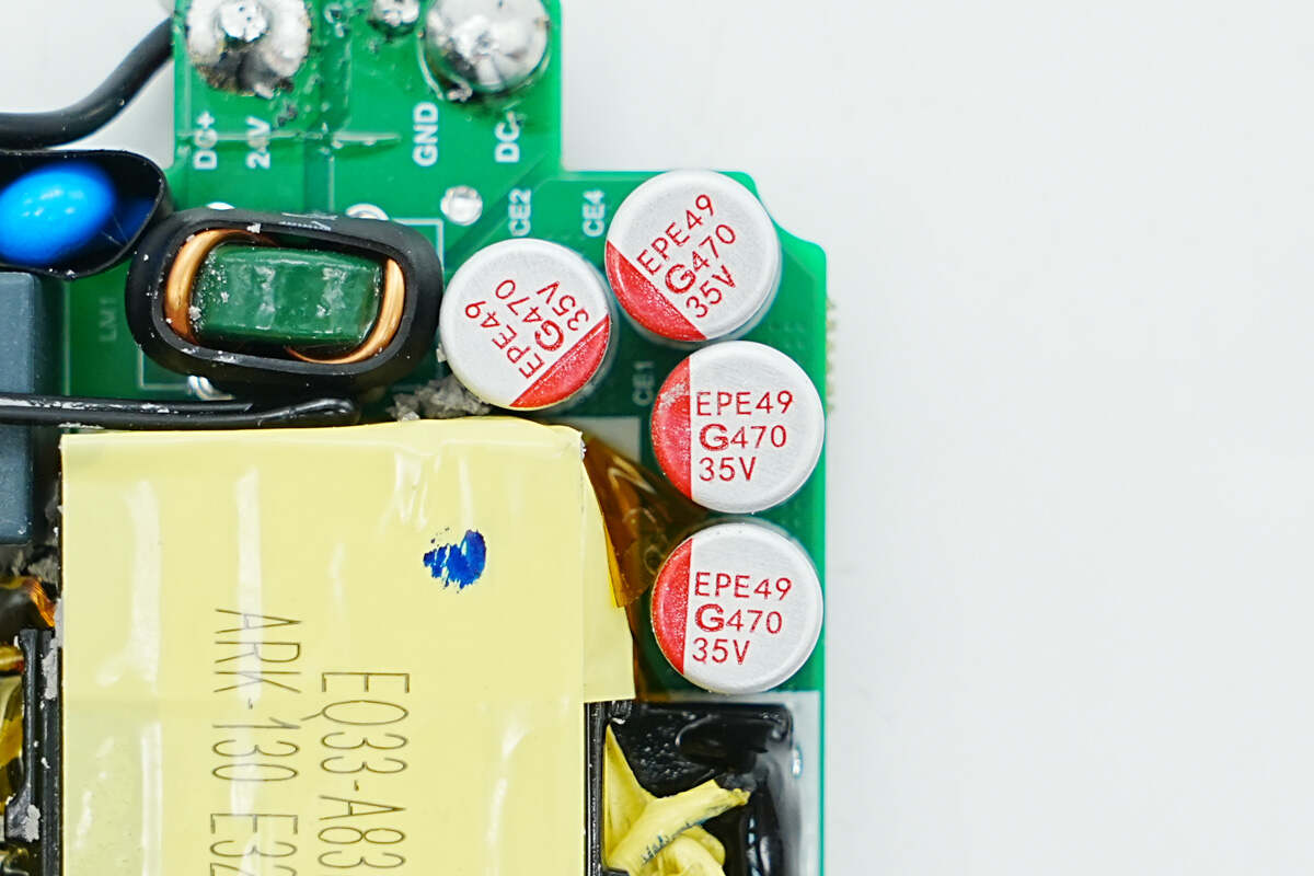
A total of four solid capacitors are connected in parallel for output filtering. 470μF 35V.
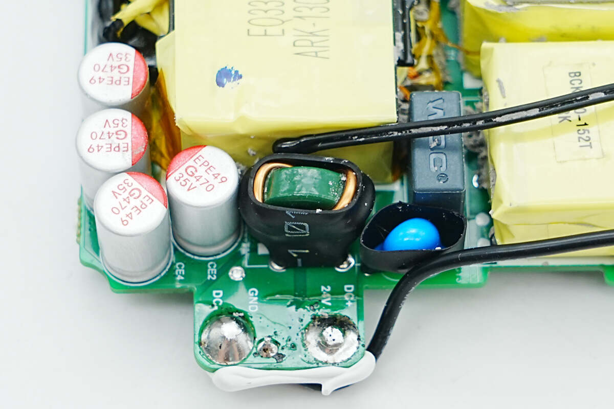
The output filter inductor is wound on a magnetic ring and insulated with heat-shrinkable tubing.
An aluminum heatsink is mounted on the lower PCB and secured with screws.
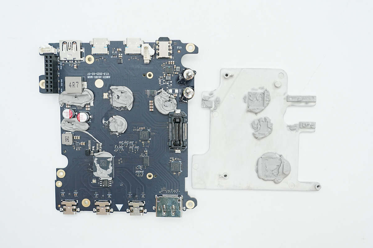
After unscrewing and removing the heatsink, thermal gel is found applied between the heat-generating chips and the heatsink.
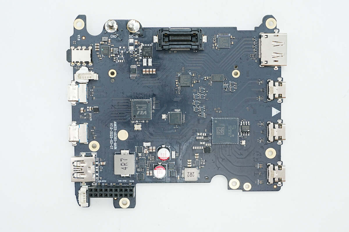
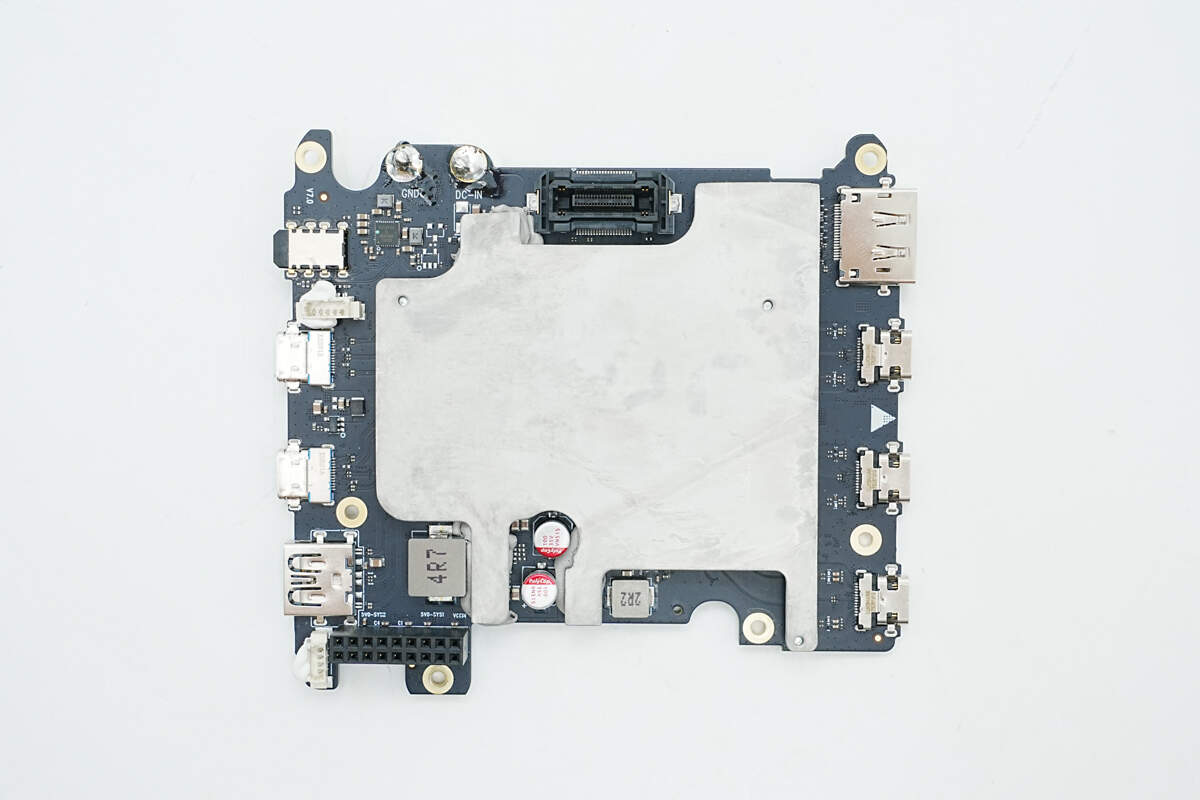
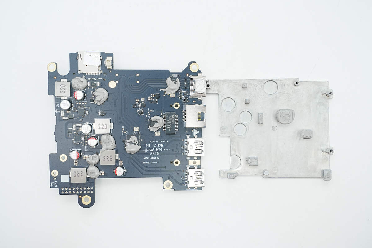
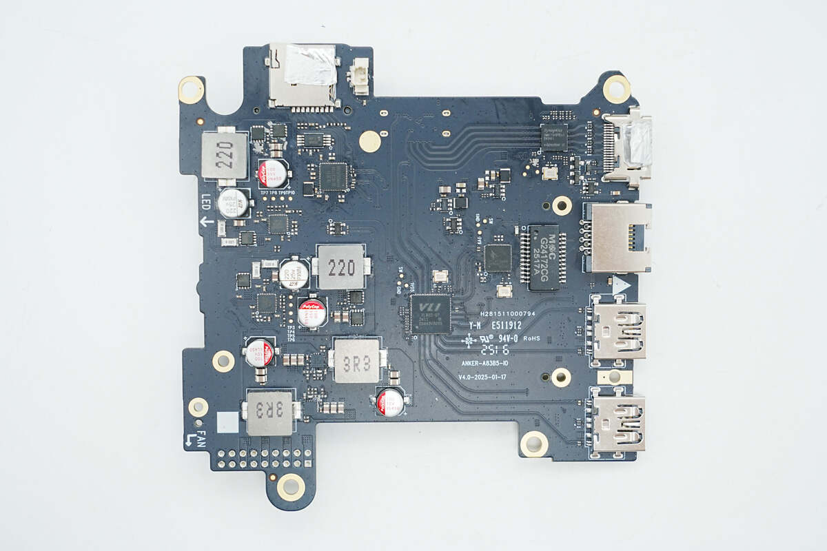
After cleaning off the thermal gel, the right side of the front of the PCB features one upstream and two downstream Thunderbolt 5 ports, as well as a DP port. In the center, there is a Thunderbolt controller, a USB hub, a video switch, and a USB-C port controller. On the left side, there is a headphone jack, a USB-C port, and two USB-A ports. In the lower left corner, there is a buck-boost converter circuit.
The back side contains memory, MCU, and a current sensor chip.
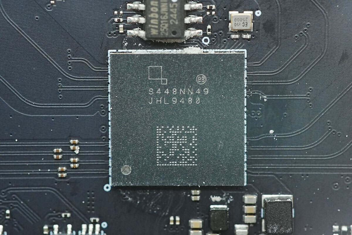
The Thunderbolt controller is from Intel and adopts the FC-CSP package. The Thunderbolt controller, codenamed Barlow Ridge, supports four PCIe lanes configured as x4 Gen 4. It features ACS, FBP, PTM, P2P, and supports 128/256-byte payloads. For DisplayPort, it provides 2 DP sinks and 3 DP sources, supports DP 2.1 tunneling and retiming, and operates in x1/x2/x4 modes with data rates ranging from 1.62 Gbps to 20 Gbps. It also includes SST, MST, DSC 1.2, FEC, LTTPR, and Panel Replay functionalities. Model is JHL9480.
This is the external buck inductor for the Thunderbolt controller.
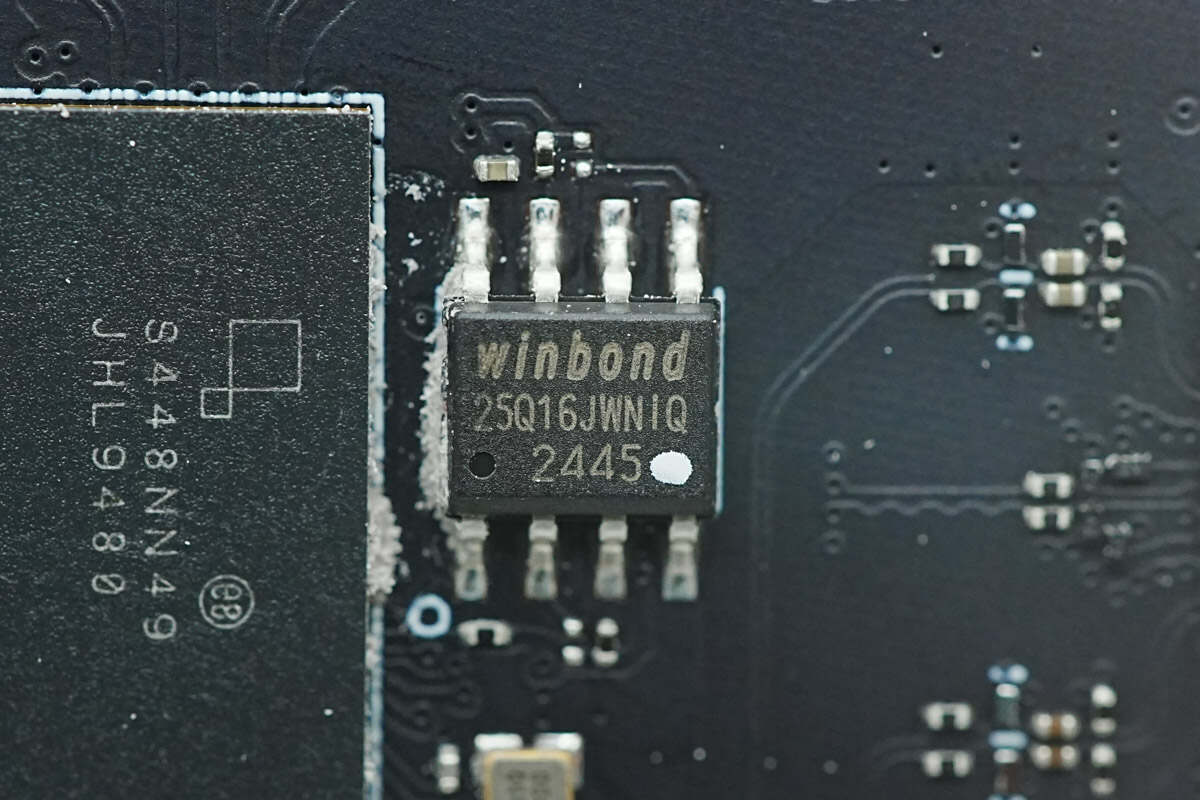
The memory is from Winbond, using an SOIC-8 package with a capacity of 2 MB. The model is W25Q16JWSNIQ.
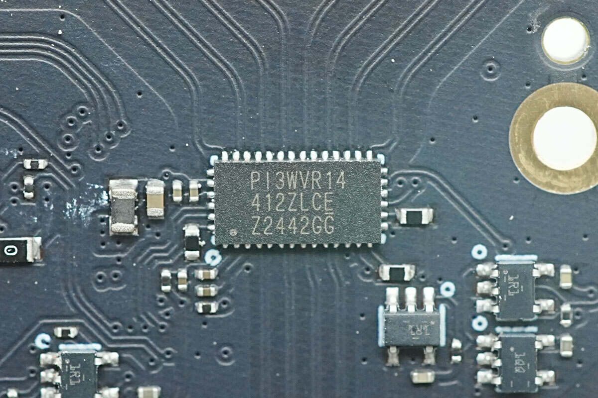
The video switch is from DIODES and comes in a TQFN40 package. It supports DP 1.3/1.4/2.0 and HDMI 2.1 interface standards, and is used for internal DP signal switching in the docking station. Model is PI3WVR14412ZLCE.
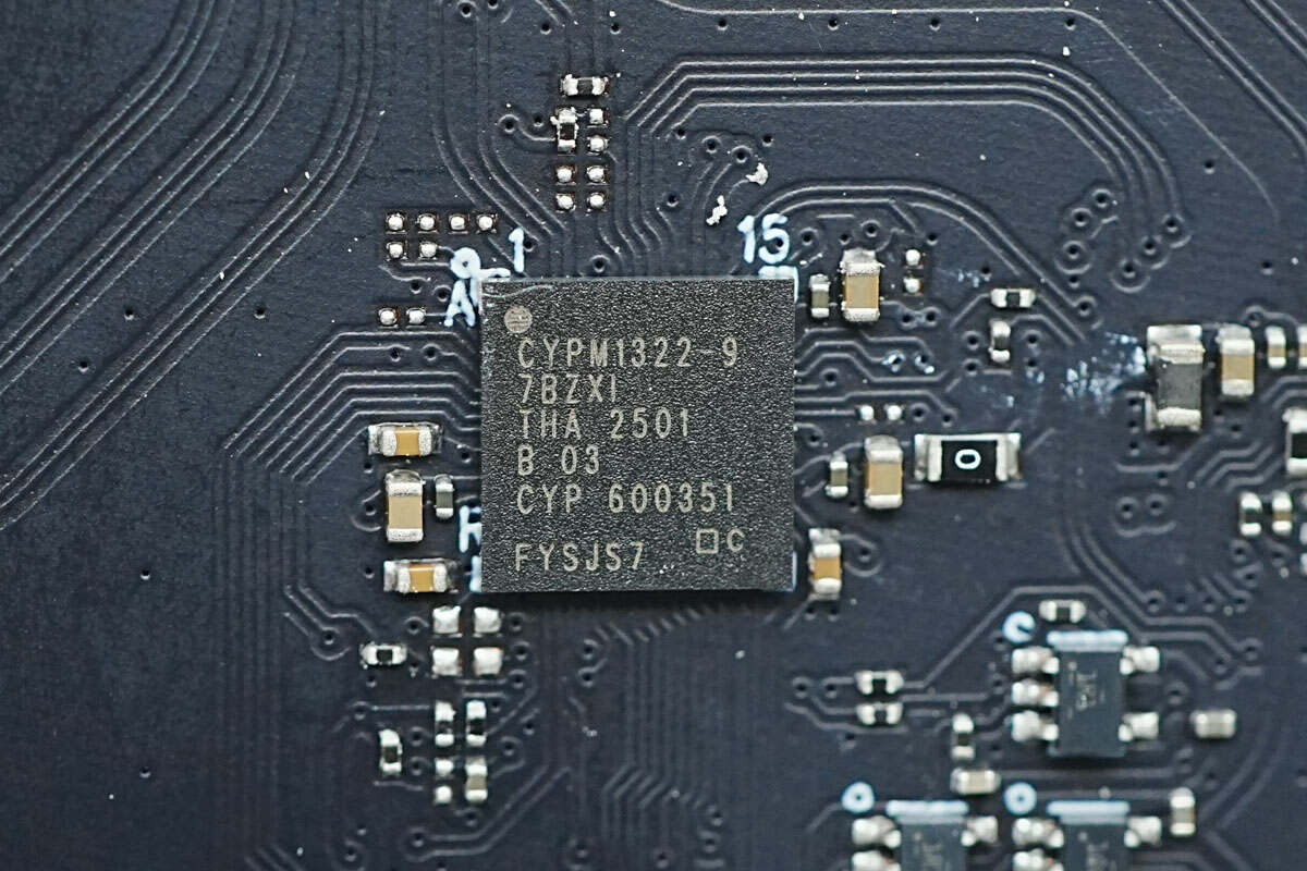
The USB-C port controller is from Infineon and uses a 97-BGA package. It belongs to the EZ-PD PMG1-S3 series of high-voltage microcontroller chips, featuring an integrated ARM Cortex-M0+ MCU with 256KB Flash and 32KB SRAM, along with built-in regulators and protection circuitry. Model is CYPM1322-97BZXI.
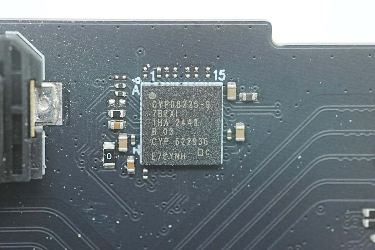
Another USB-C port controller is also from Infineon, part of the EZ-PD CCG8 series, also in a 97-BGA package. It supports PD 3.1 28V EPR applications, includes an ARM Cortex-M0+ MCU with 256KB Flash and 32KB SRAM, and supports dual-port control. Model is CYPD8225-97BZXI.
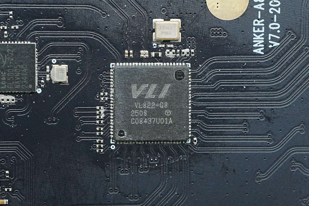
The USB hub chip is from VIA Labs and uses a QFN 88L package. It integrates an upstream port and two downstream port multiplexers, making it suitable for expansion with two USB-A and two USB-C ports, and supports data rates up to 10 Gbps. Model is VL822-Q8.
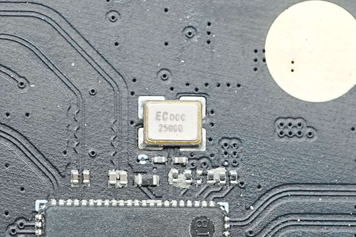
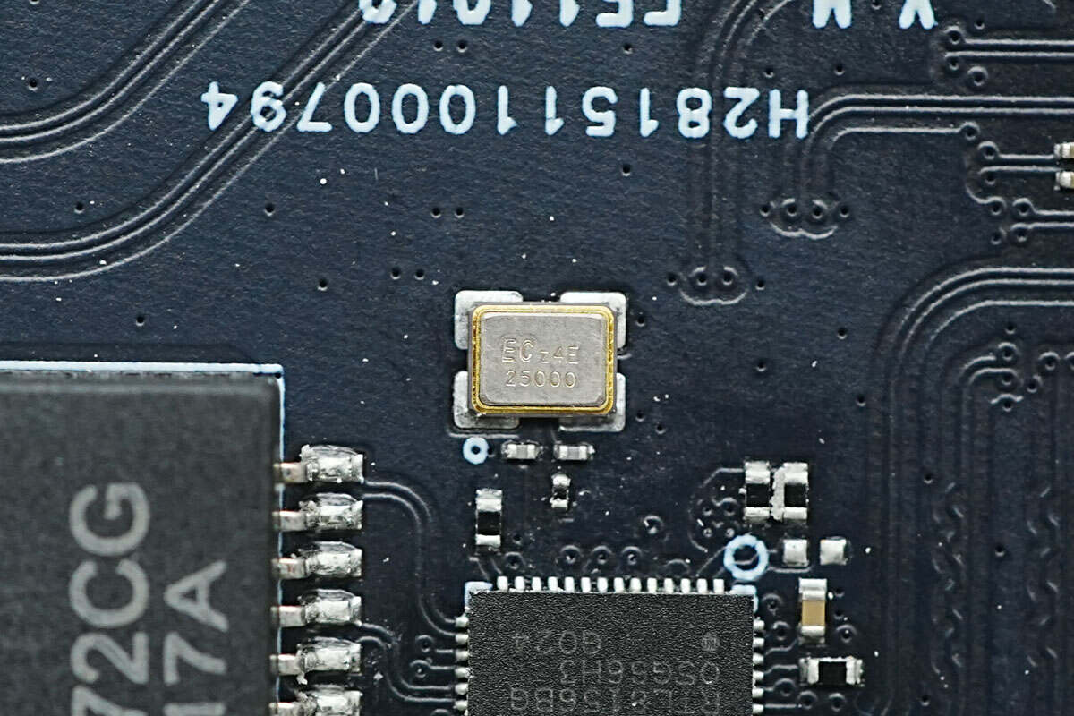
This is an external 25.000 MHz clock crystal oscillator.
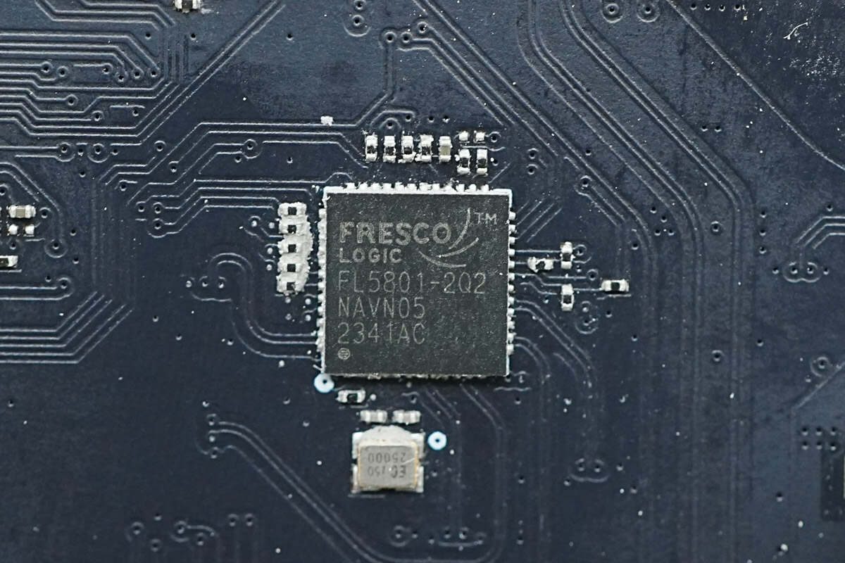
The hub chip is from Parade Technologies and uses a QFN48 package. It is a USB 2.0 hub that supports either one upstream and five downstream ports or two upstream and four downstream ports. It is backward compatible with USB 1.1, supports the BC1.2 specification, and allows for feature customization. Model is FL5801-2Q2.
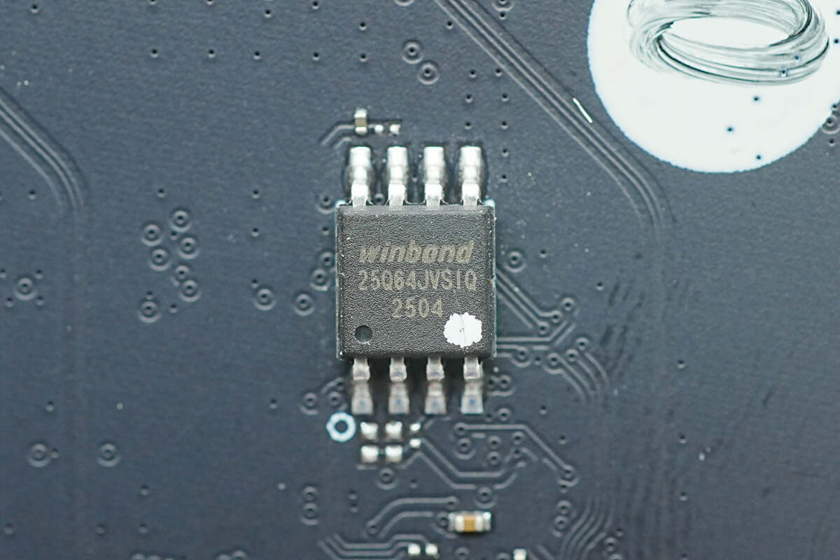
The memory is from Winbond, uses an SOIC-8 package, and has a capacity of 8 MB. Model is W25Q64JVSSIQ.
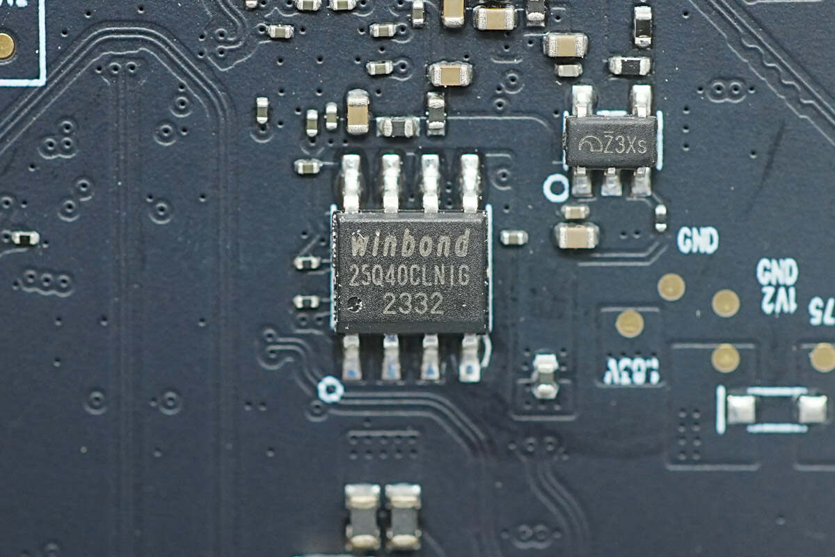
The memory is from Winbond, uses an SOIC-8 package, and has a capacity of 512 KB. Model is W25Q40CLSNIG.
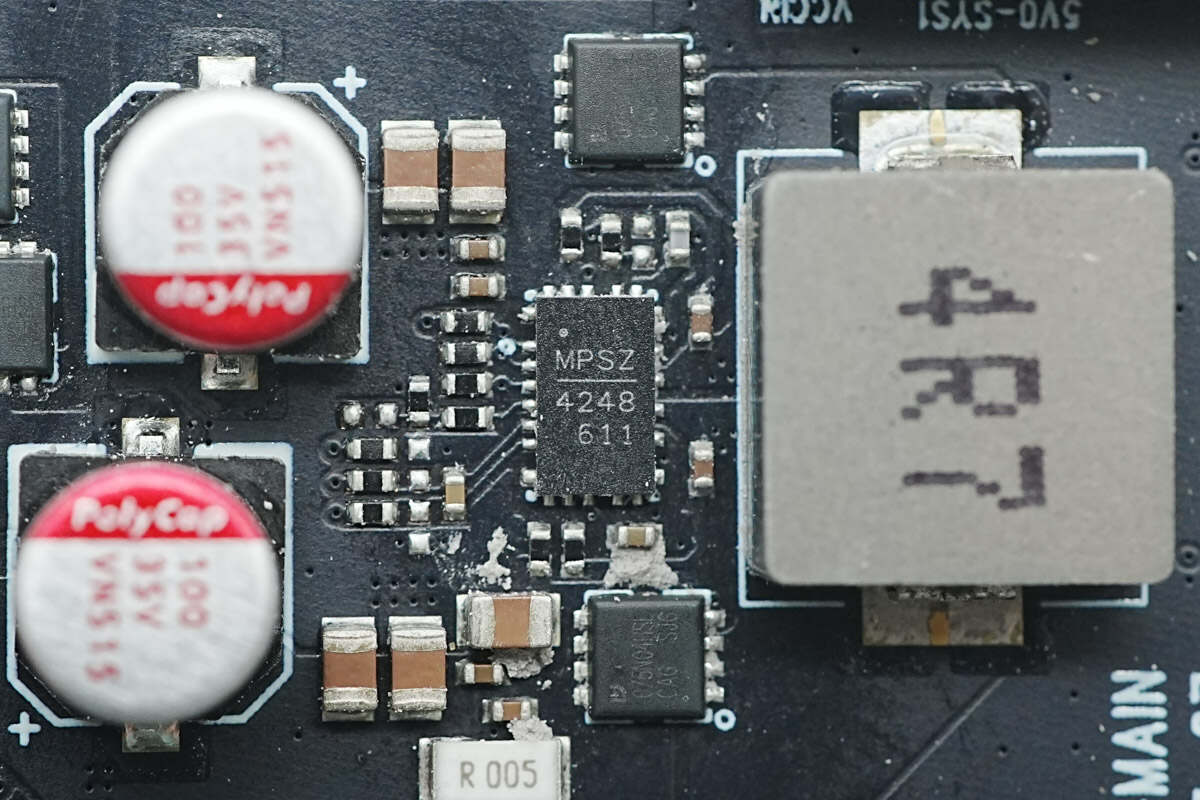
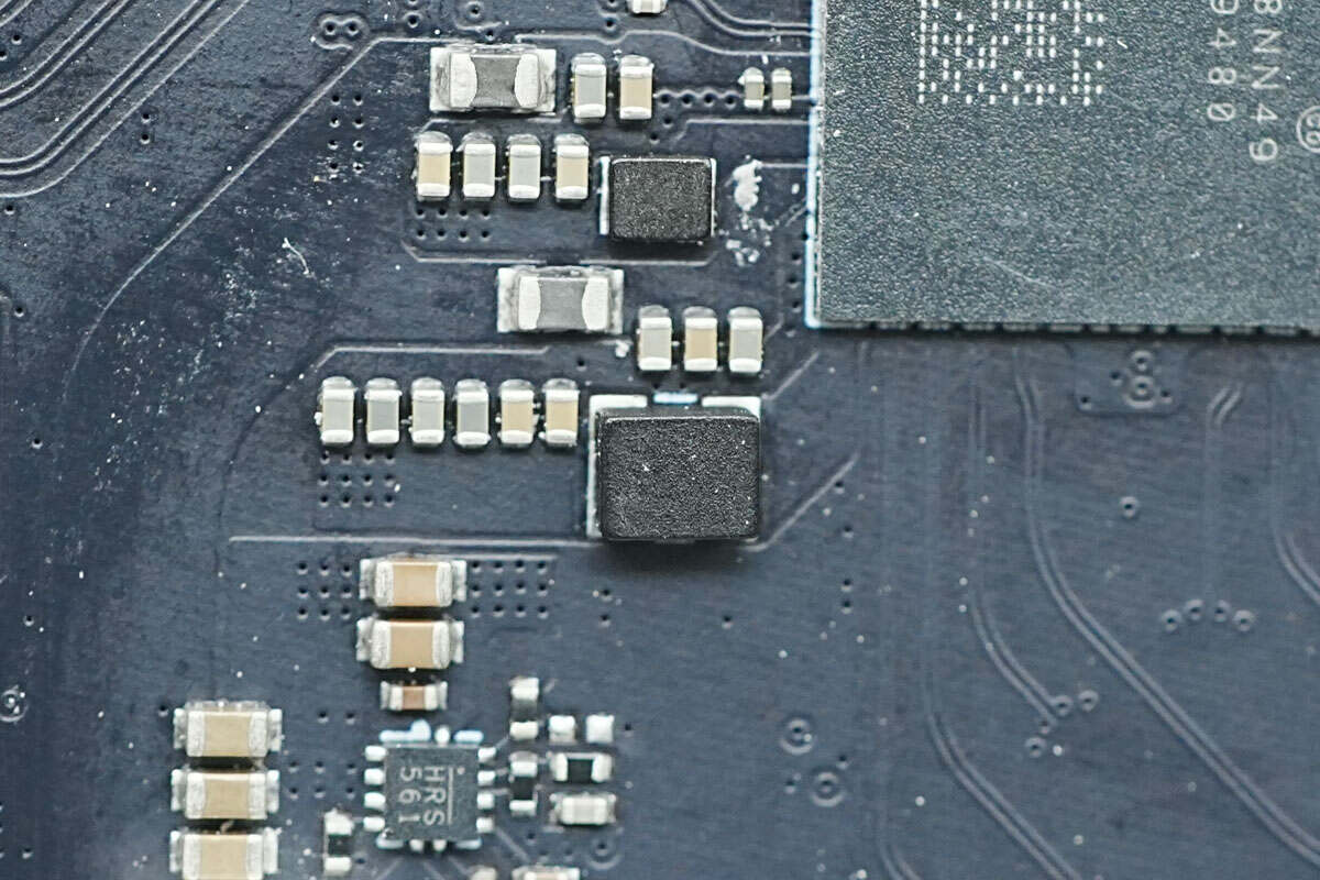
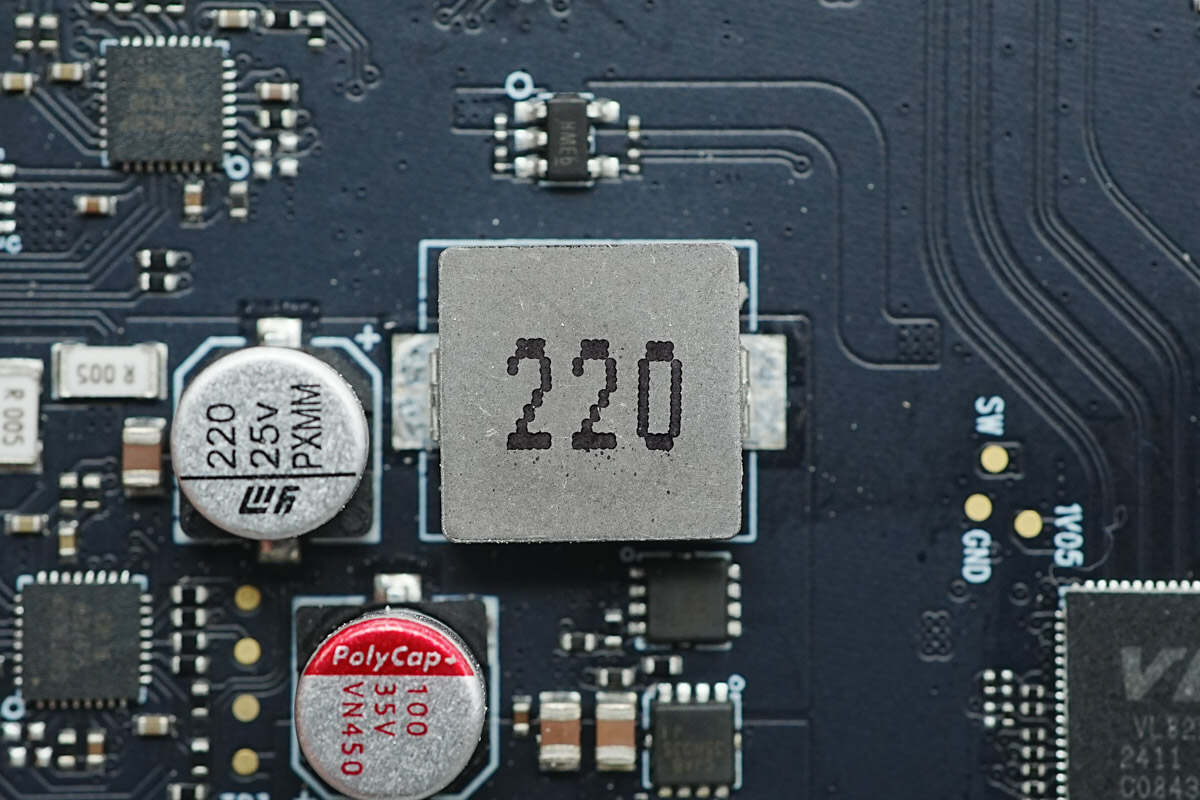
The synchronous buck-boost chip used for the 140W output of the Thunderbolt 5 upstream port is from MPS and adopts a QFN 3×5-20 package. It is an integrated synchronous buck-boost converter with two built-in low-side MOSFETs and an external high-side driver. The chip supports up to 140W output power and handles input and output voltages up to 36V. It can interface with a protocol controller via I²C. Model is MP4248.
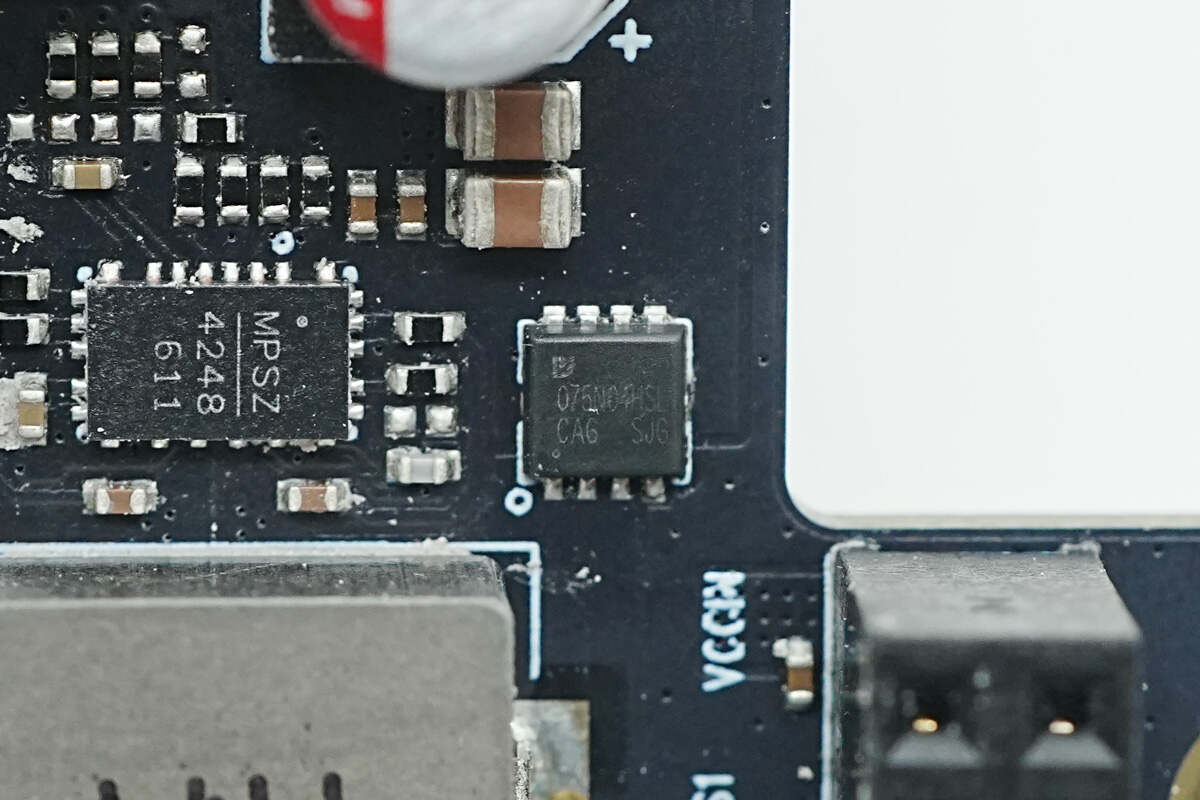
The external PMOSFET on the input side is from Pingwei and marked with 075N04HSL.
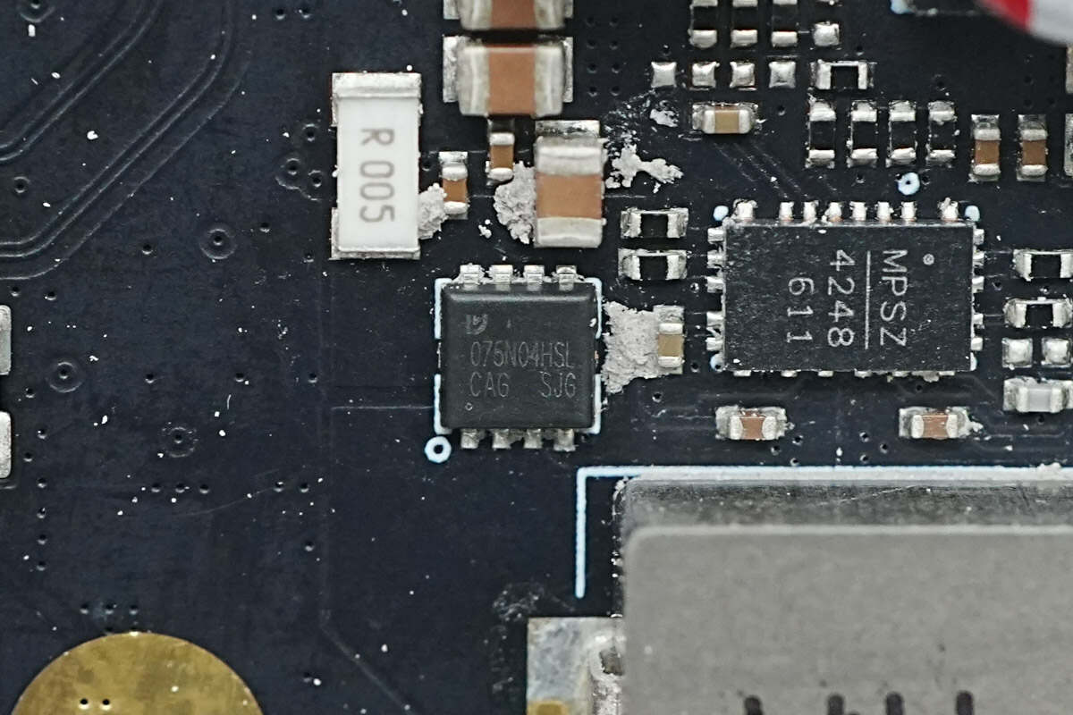
The PMOSFET at the output has the same model.
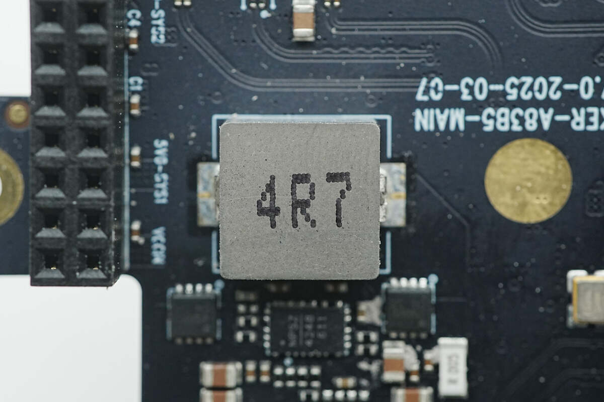
The alloy inductor is used for the buck-boost conversion. 4.7μH.
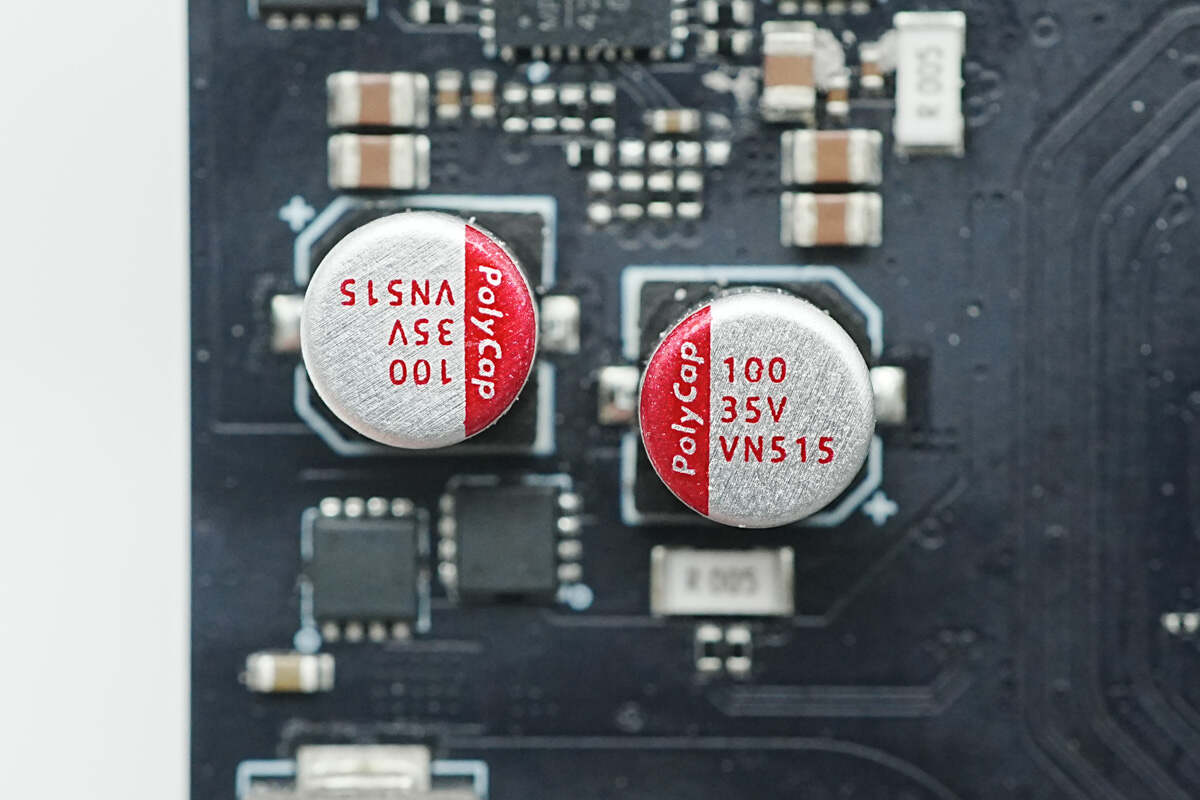
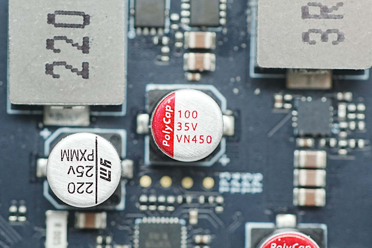
The filtering capacitors are from PolyCap’s VN series, a compact product line. Two capacitors of the same specifications are used separately for output and output filtering. 100μF 35V.
The VBUS MOSFET is from Pingwei and marked with 075N04HSL.
The synchronous buck chip is from MPS and comes in a QFN-11 package. It integrates MOSFETs internally, supports a 24V input voltage, provides a continuous output current of 4A, operates at a switching frequency of 700kHz, supports ceramic capacitor filtering, and includes comprehensive protection features. Model is MP2384.
This is the alloy inductor. 2.2μH.
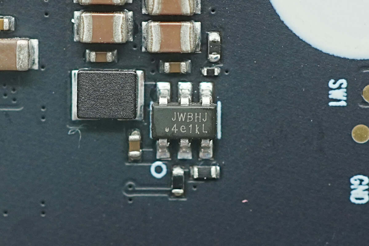
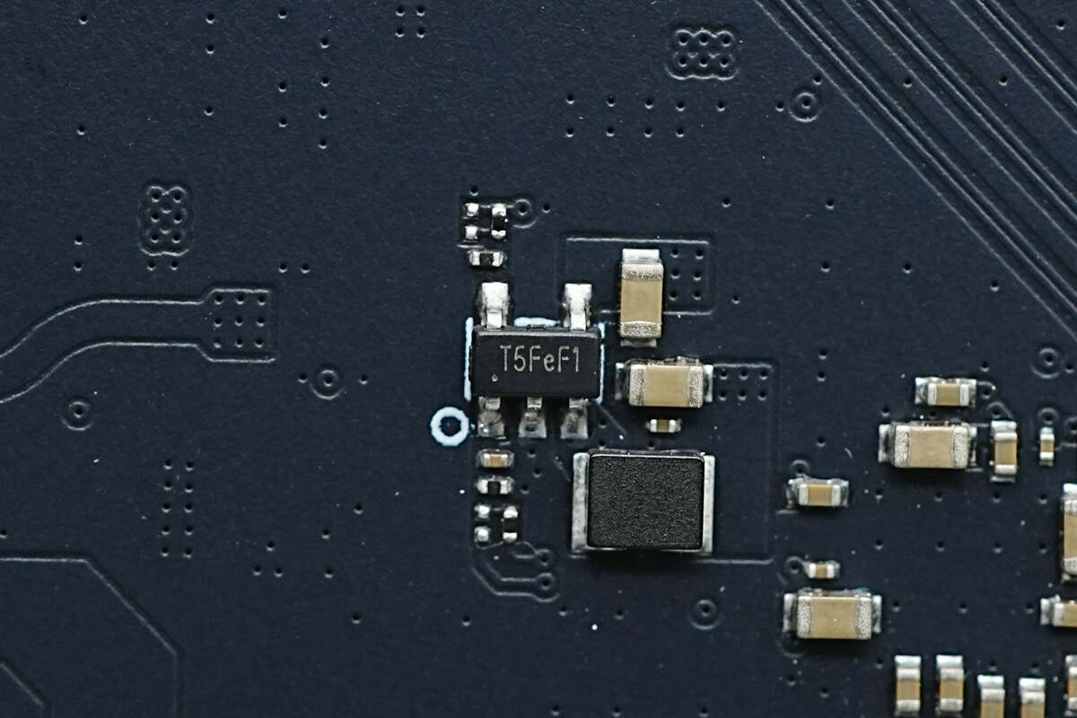
The synchronous buck converter marked with JWBH is from JOULWATT and uses a SOT23-6 package. It is a synchronous buck converter with a 40V voltage rating, 1A output current, and a fixed switching frequency of 1.1MHz. It features input undervoltage lockout, integrated soft-start, current limit protection, short-circuit protection, and over-temperature protection. Model is JW5026.
Here is the information about JOULWATT JW5026.
This is another JW5026 synchronous buck converter.
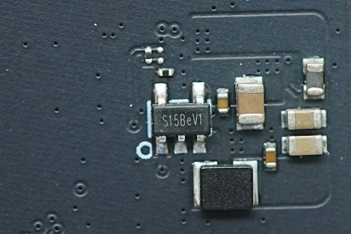
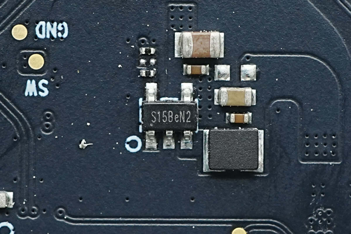
The synchronous buck chip marked with S15B is from Tollsemi and adopts the SOT23-5 package. It supports a 5.5V input voltage, delivers an output current of 1.2A, operates at a switching frequency of 1.5MHz, and features input overvoltage protection, short-circuit protection, and over-temperature protection. Model is TMI3410.
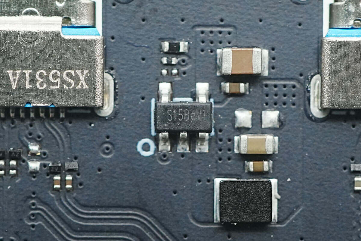
This is another TMI3410 synchronous buck chip.
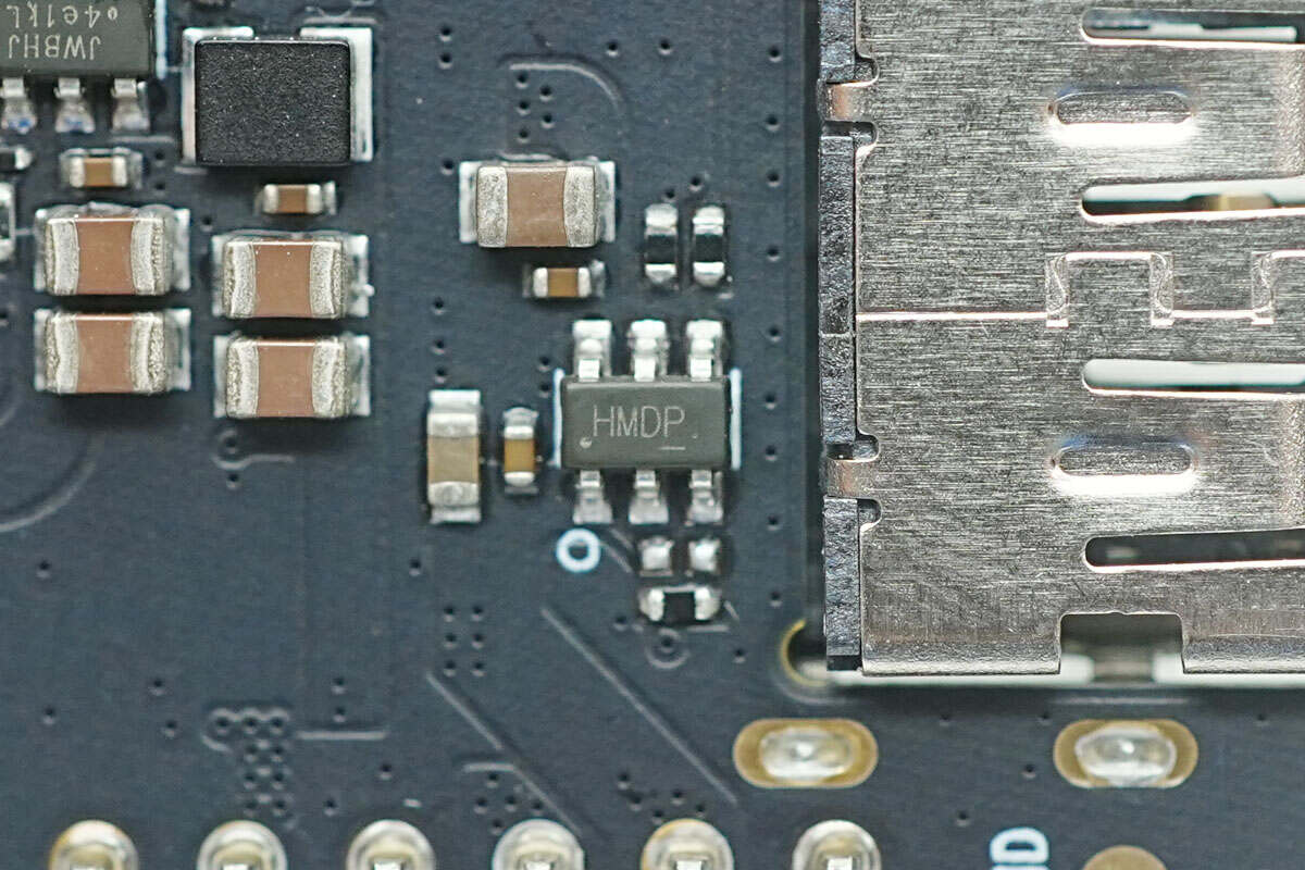
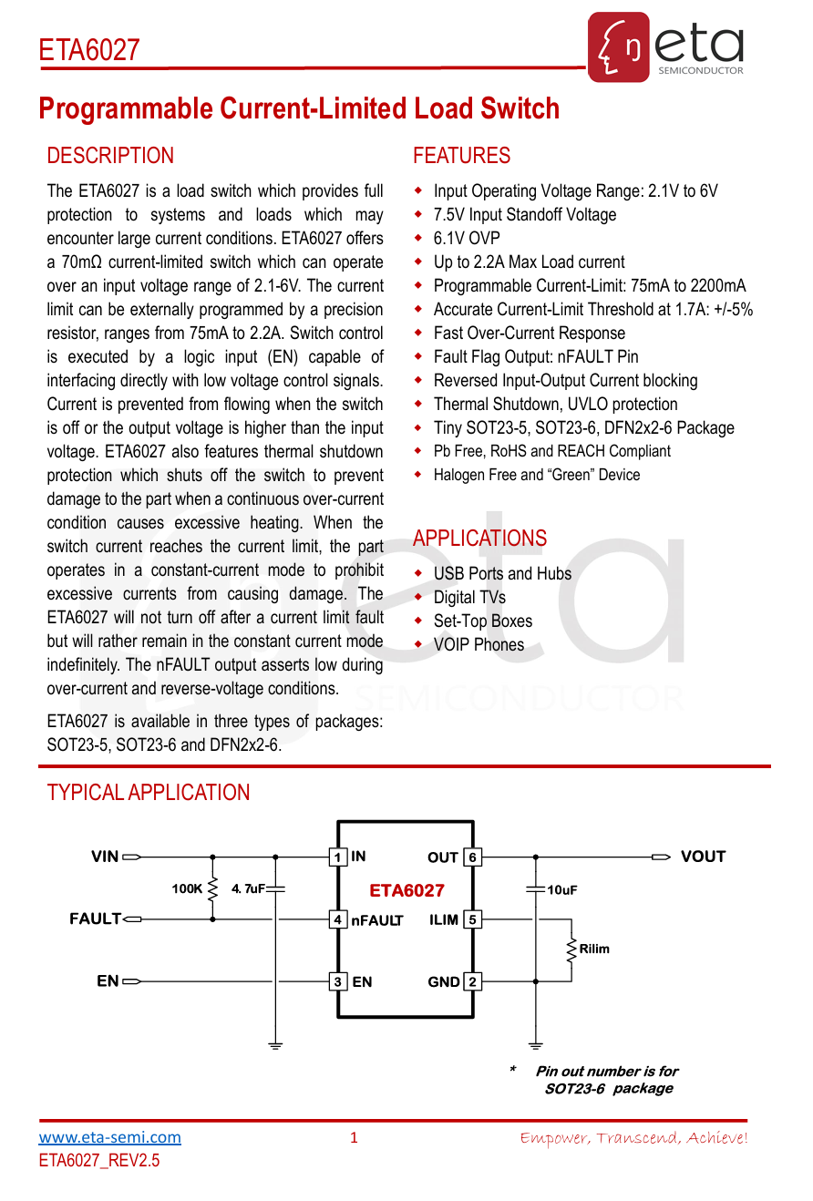
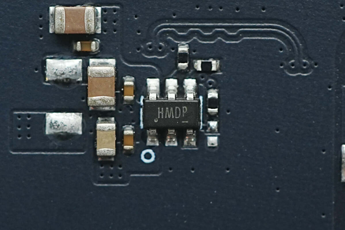
The overcurrent protection chip marked with HM is from ETA and adopts the SOT23-6 package. It is a load switch with programmable current protection. The chip supports a 6V input voltage, features 6.1V overvoltage protection, adjustable current limits from 75mA to 2.2A, fast overcurrent protection, reverse current blocking, over-temperature shutdown, and undervoltage protection. Model is ETA6027.
Here is the information about ETA ETA6027.
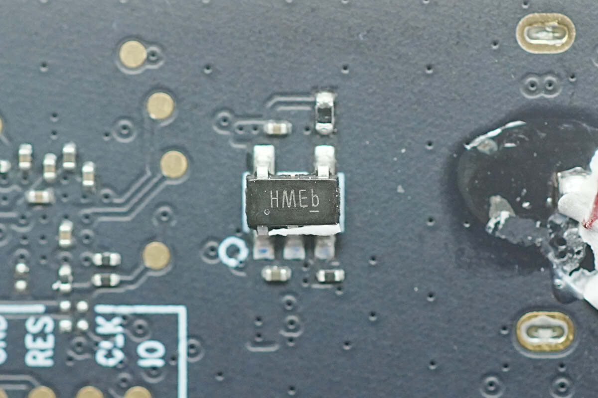
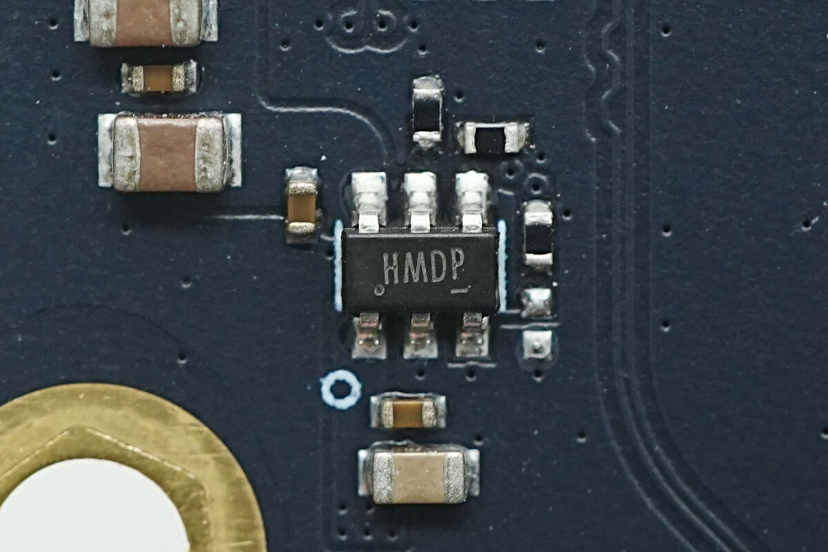
This is another ETA6027 overcurrent protection chip.
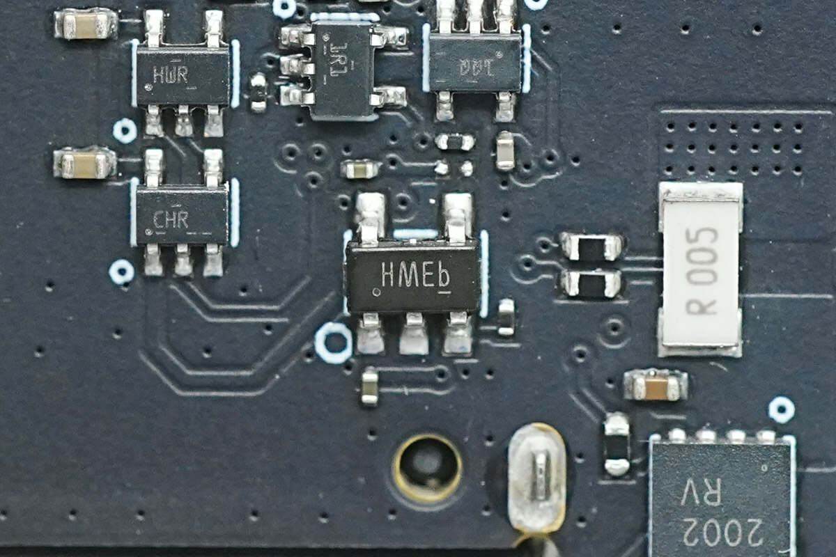
This is the ETA6027 overcurrent protection chip.
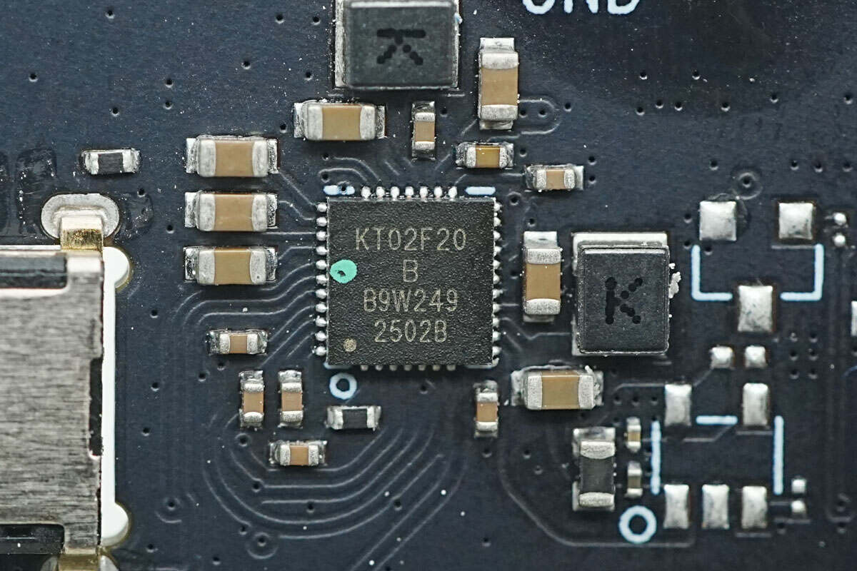
The USB audio chip is from KTMicro and uses a QFN36 package. It is a single-chip USB audio codec. Model is KT02F20.
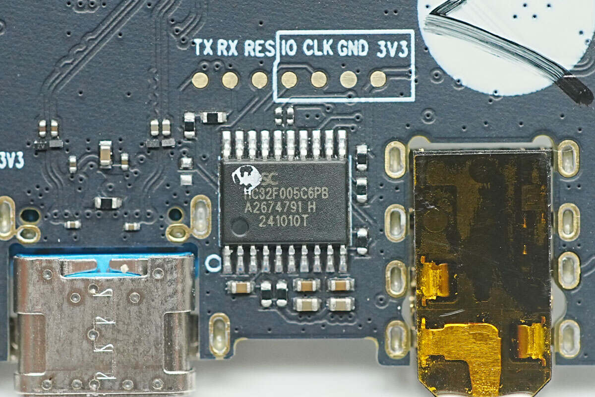
The MCU is from XHSC and adopts the TSSOP20 package. It features a built-in ARM Cortex-M0+ 32-bit CPU running at 32MHz, with 32KB Flash and 4KB SRAM, and supports UART, SPI, and I2C communication interfaces. Model is HC32F005C6PB.
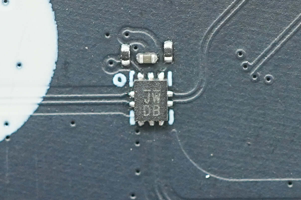
The switch is marked with JW.
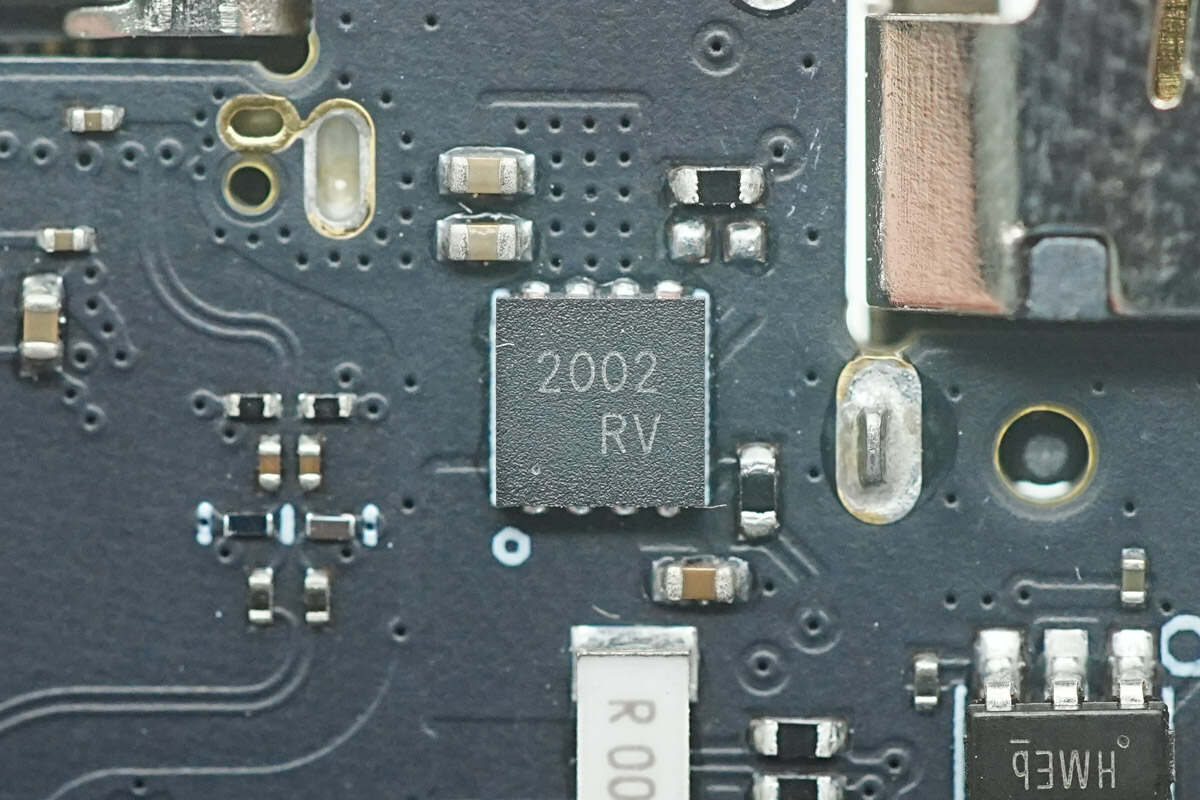
The MOSFET marked with 2002 is used for power control.
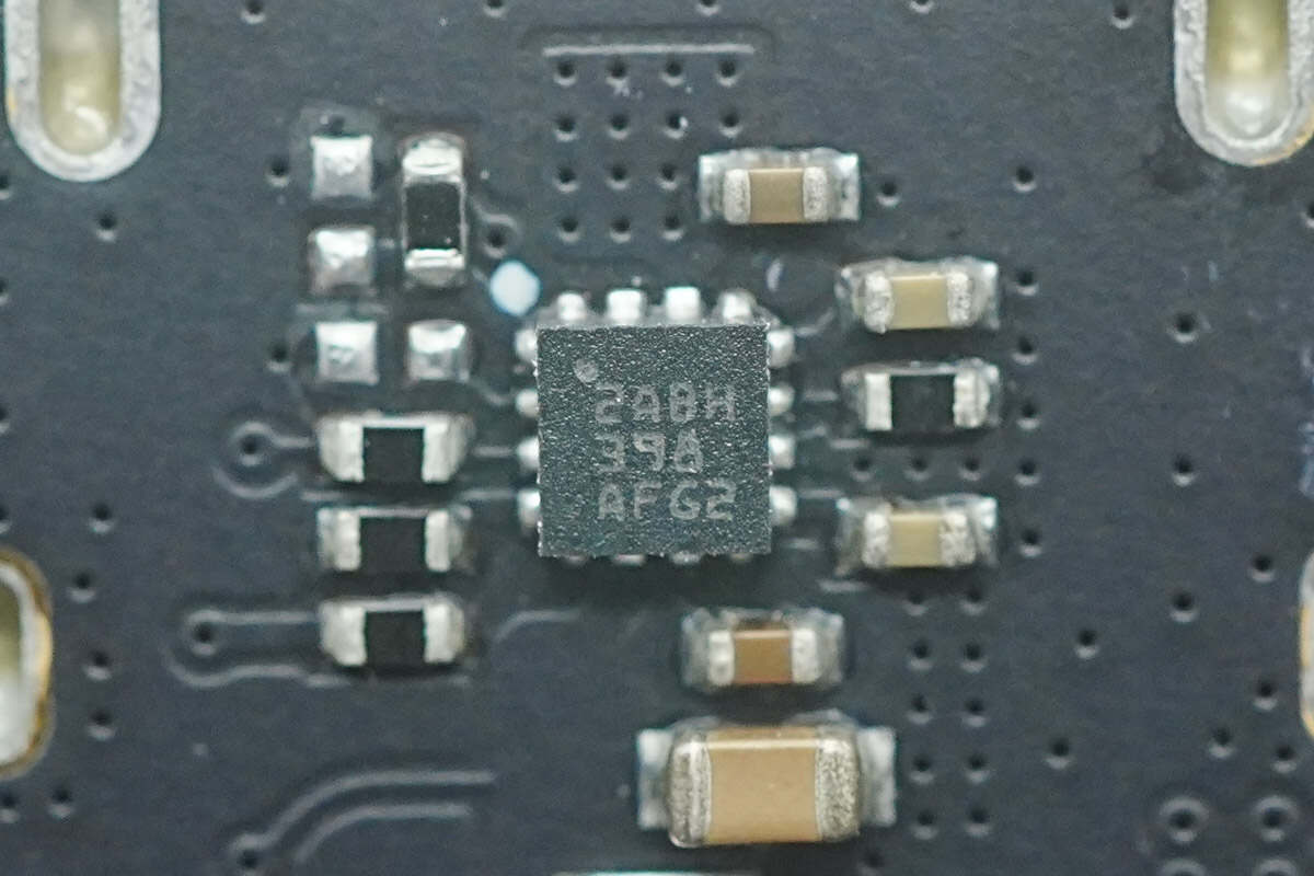
The overcurrent protection chip marked with 2ABH is from TI and adopts the QFN2*2 package. It supports a 23V operating voltage and a 6A operating current. The overvoltage clamp threshold and overcurrent protection threshold are adjustable. It features an adjustable output slew rate control and includes over-temperature protection. The device is certified to the IEC 62368-1 CB safety standard. Model is TPS259472.
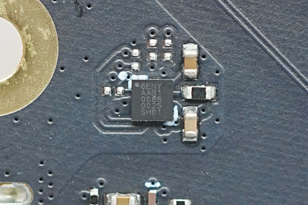
The chip marked with 6ENY is the AAB1 chip.
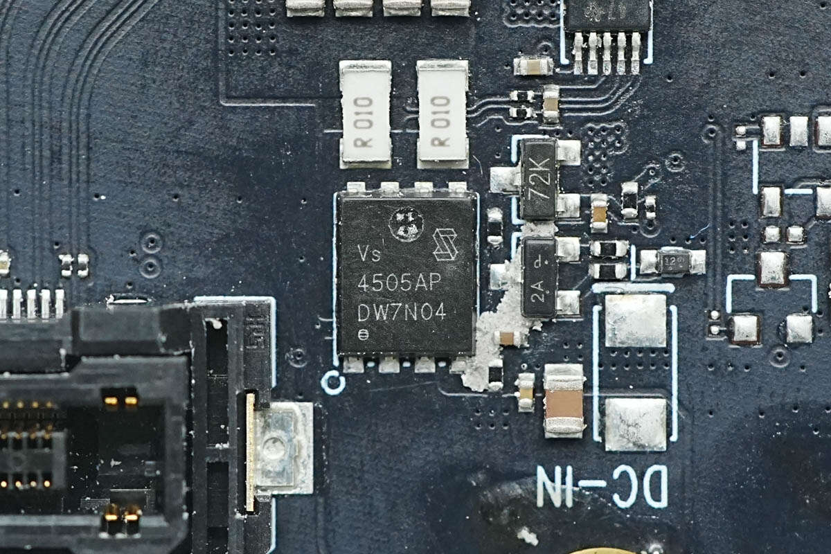
The MOSFET used for power control is from Vergiga, a PMOS device, and comes in a PDFN 5×6 package. -40V 8.7mΩ. Model is VS4505APT.
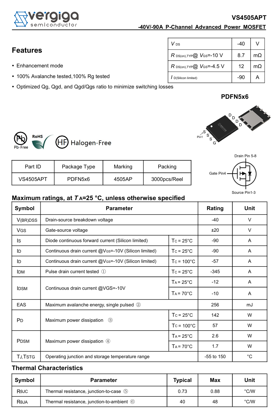
Here is the information about Vergiga VS4505APT.
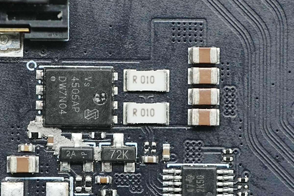
Two 10mΩ resistors are connected in parallel for current sensing.
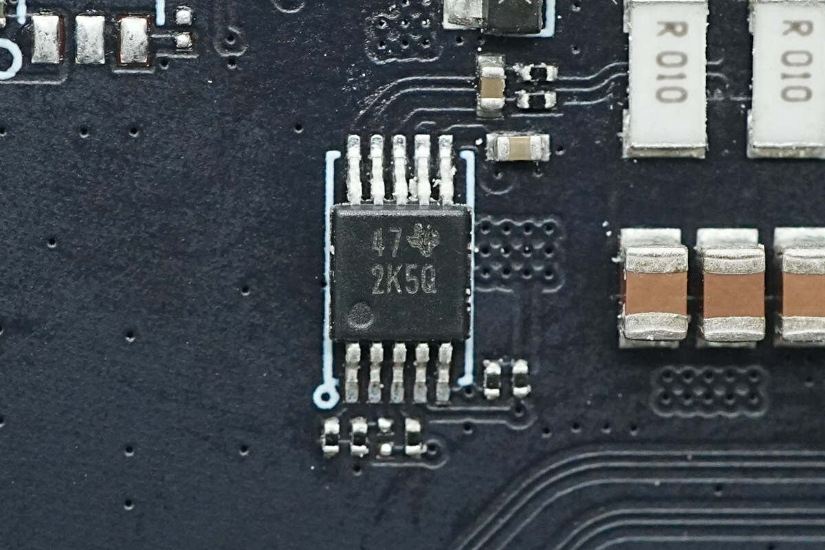
The digital power monitor marked with 2K5Q is from TI and comes in a VSSOP10 package. It supports a 36V bus voltage, allows for high-side or low-side current sensing, and provides current, voltage, and power reporting. Model is INA230.
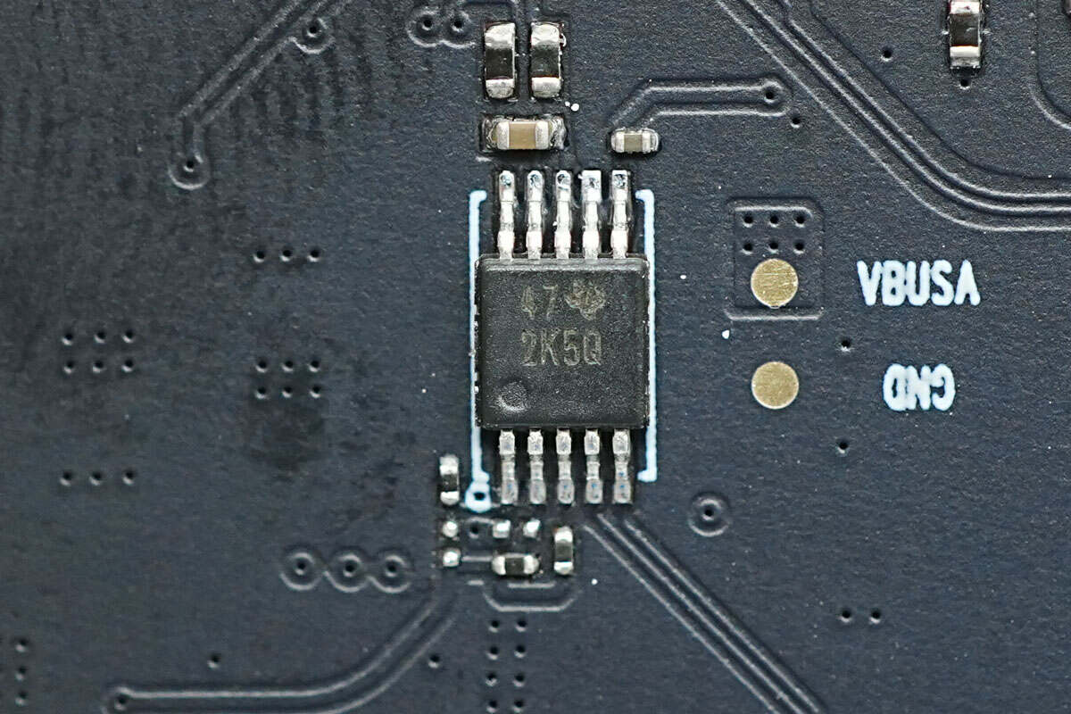
This is another INA230 digital power monitor.
An aluminum heatsink is mounted on the top PCB and secured with screws.
After unscrewing and removing the heatsink, thermal gel is found applied between the heat-generating chips and the heatsink.
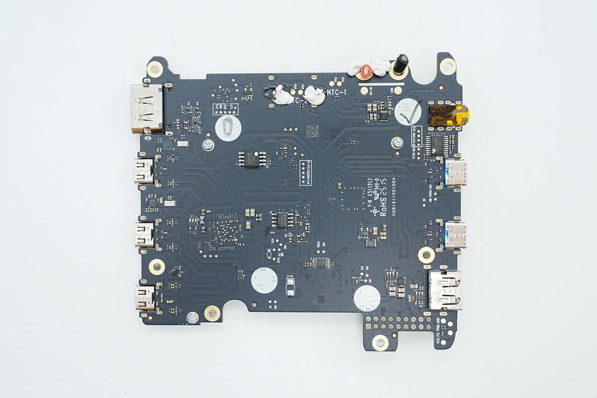
On the left side of the PCB, there are four synchronous buck circuits, each dedicated to one of the four USB-C ports. Above them is a TF card slot and its card reader chip. In the middle sits the hub chip. On the upper right side is the video conversion chip, with the Ethernet controller chip and network transformer below it. Also on the right side are the HDMI port, Ethernet port, and USB-A port.
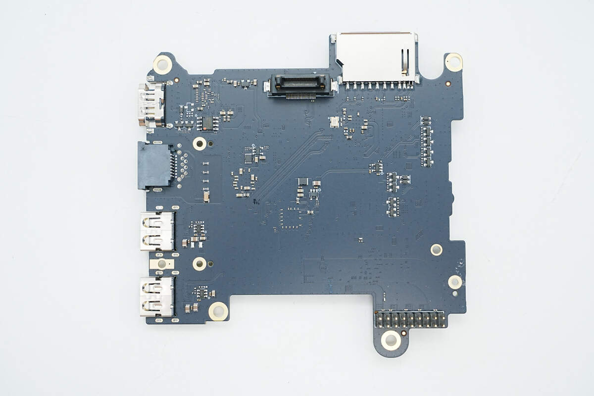
The back features a high-speed connector, memory modules, and an SD card slot.
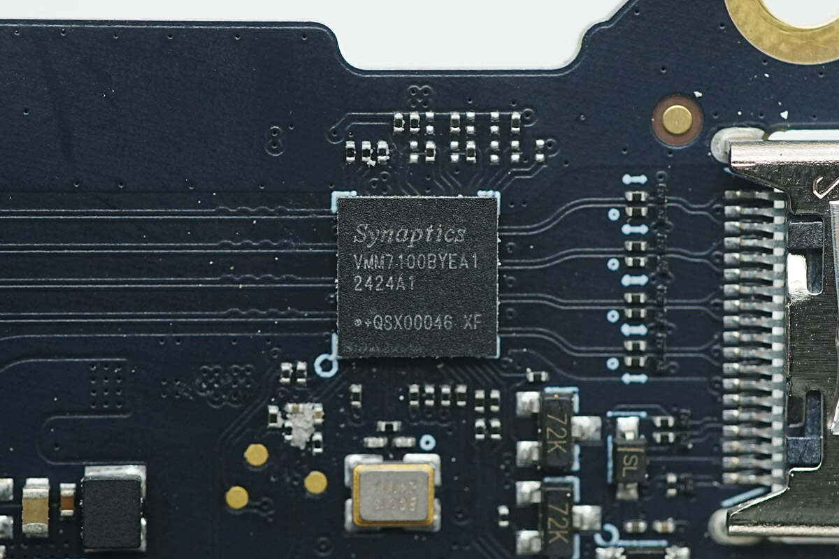
The video conversion chip is from Synaptics and uses an 81-BGA package. It converts DP signals to HDMI video output, supporting up to 8K at 60Hz or 4K at 240Hz resolution. Model is VMM7100.
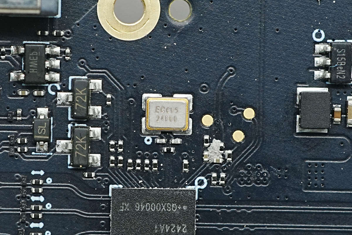
This is an external 24.000 MHz clock crystal oscillator.
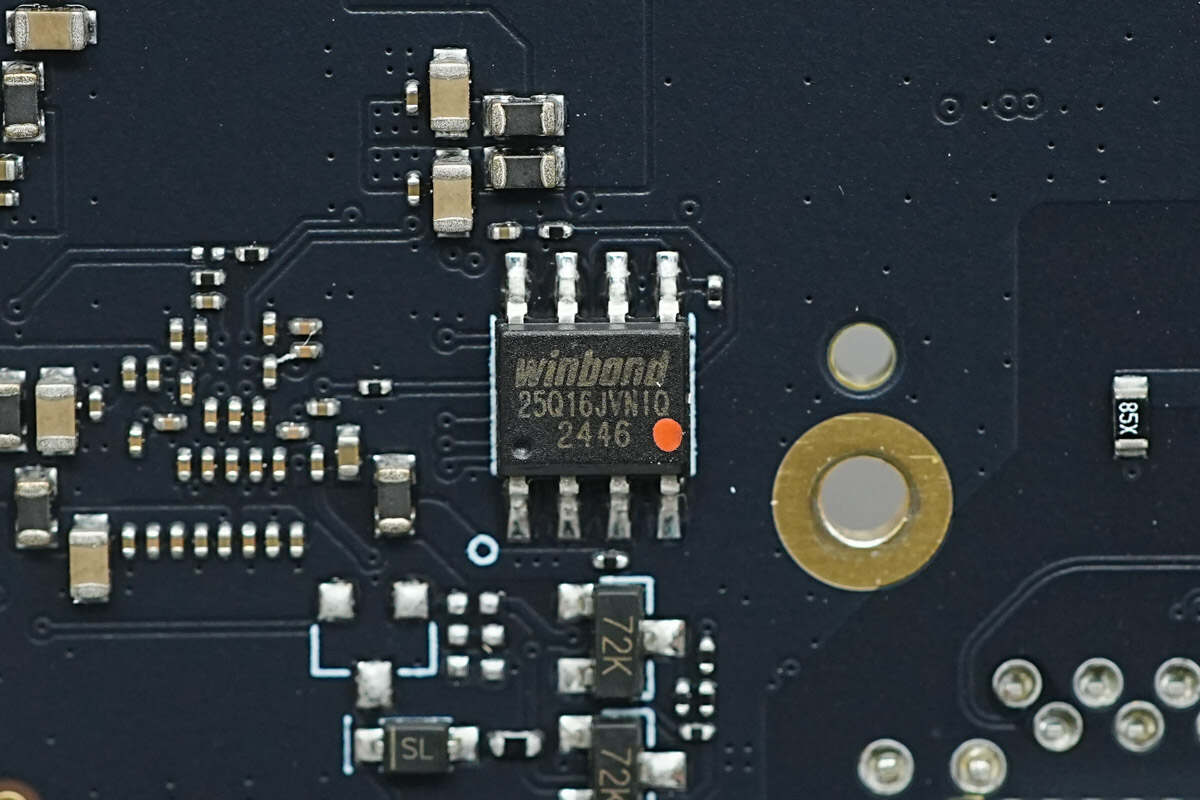
The memory is from Winbond, with a capacity of 2MB, and uses an SOIC-8 package. Model is W25Q16JVSNIQ
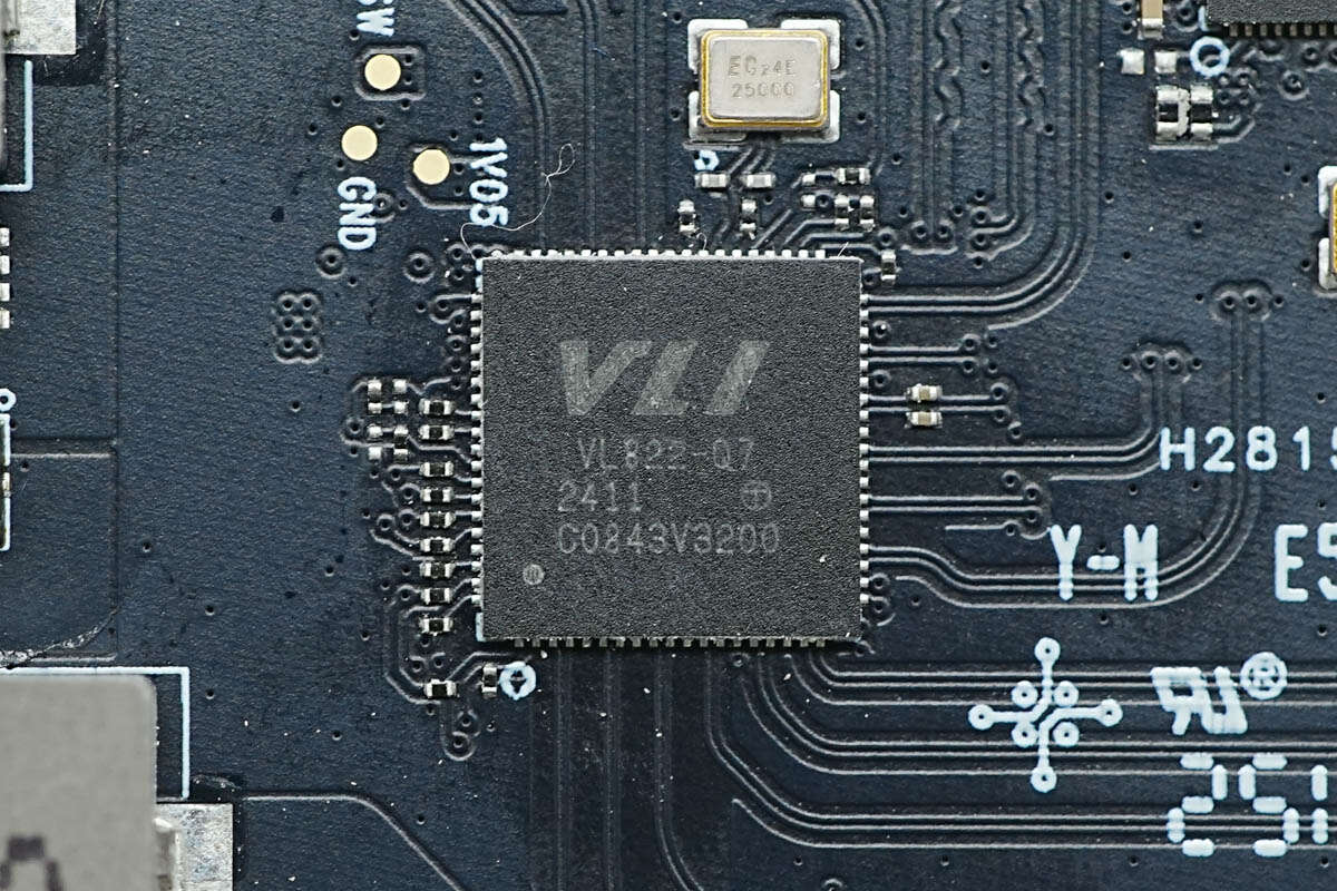
The USB hub chip is from VIA Labs, integrates one upstream port and two downstream port multiplexers, suitable for expanding four USB-A ports, supports 10Gbps data rates, and comes in a QFN 76L package. Model is VL822-Q7
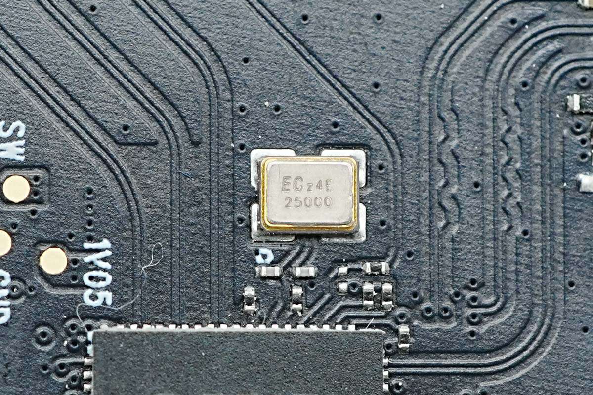
This is an external 25.000 MHz clock crystal oscillator.
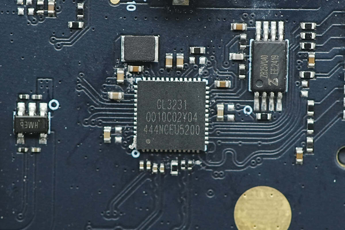
The card reader chip is from GENESYS. It is a USB 3.1 Gen1 to dual SD 3.0 LUN storage card reader controller, integrates a DC-DC converter and comes in a QFN52 package. Model is GL3231.
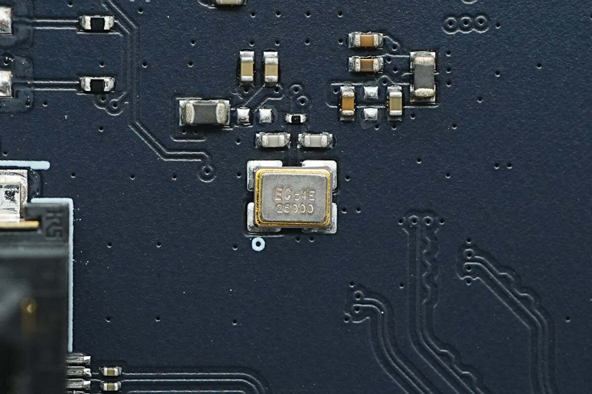
This is an external 25.000 MHz clock crystal oscillator.
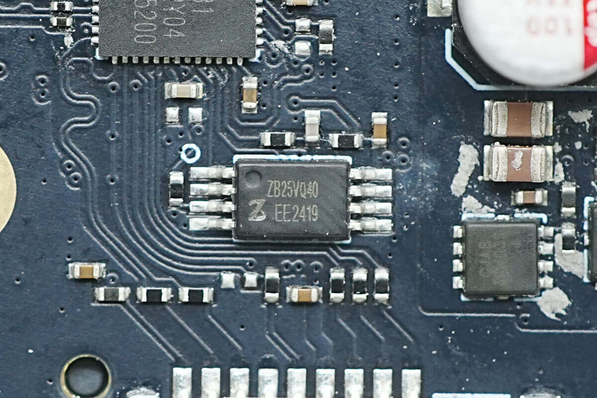
The memory is from Zbit, with a capacity of 512KB, and uses a TSSOP8 package. Model is ZB25VQ040.
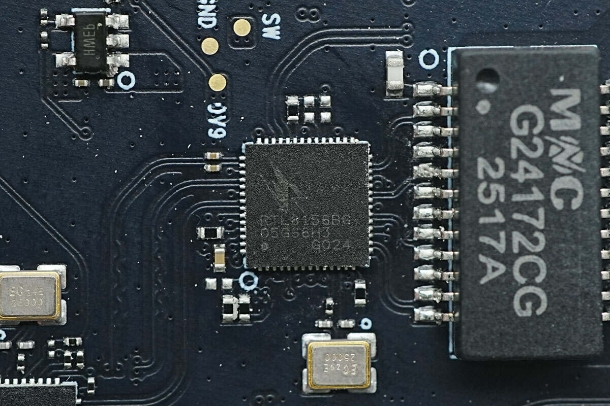
The 2.5G Ethernet chip is from REALTEK, used for USB 3.0 to 2.5G wired networking, backward compatible with Gigabit and 100 Mbps speeds, and comes in a QFN56 package. Model is RTL8156BG.
This is an external 25.000 MHz clock crystal oscillator.
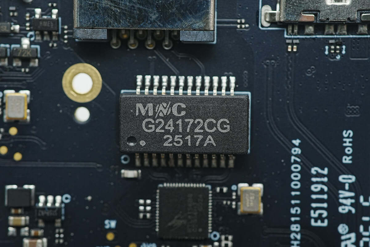
The network transformer is from Mentech, supports 2.5G transmission speeds, and is an SMD type. Model is G24172CG.
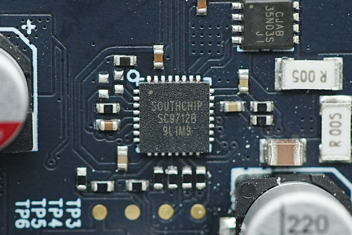
The protocol buck converter chip for the front dual USB-C fast charging ports is from SouthChip. It is a highly integrated dual-port fast charging SoC that integrates a 36V high-efficiency synchronous buck controller, one Type-C interface, and two DPDM fast charging protocol interfaces, supporting the UFCS fast charging protocol. The SC9712B supports dual-chip collaboration: it delivers full power output when operating a single port and automatically allocates power when both ports operate simultaneously. It requires no MCU control and comes in a QFN-32 package. Model is SC9712B.
The circuitry for the two USB-C ports is identical; to save space, only one port is described here.
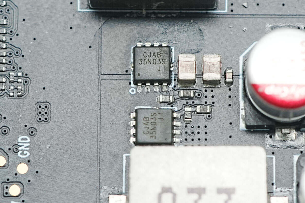
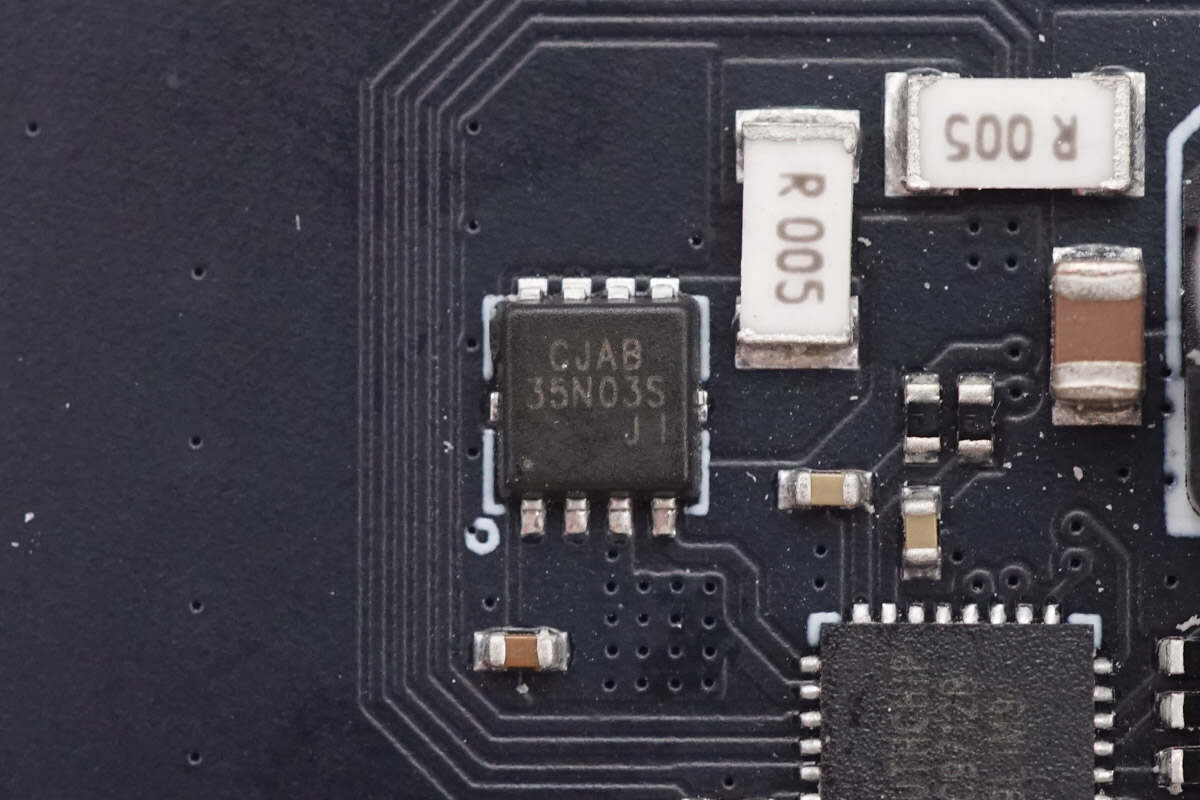
The synchronous buck MOSFET is from JSCJ, an NMOS with a 30V voltage rating and 5.2mΩ on-resistance. It comes in a PDFNWB 3.3×3.3-8L package. Model is CJAB35N03S.
This is a 22μH alloy inductor.
The filter capacitor is from PolyCap’s VN series, a compact product line, with a specification of 100μF, 35V.
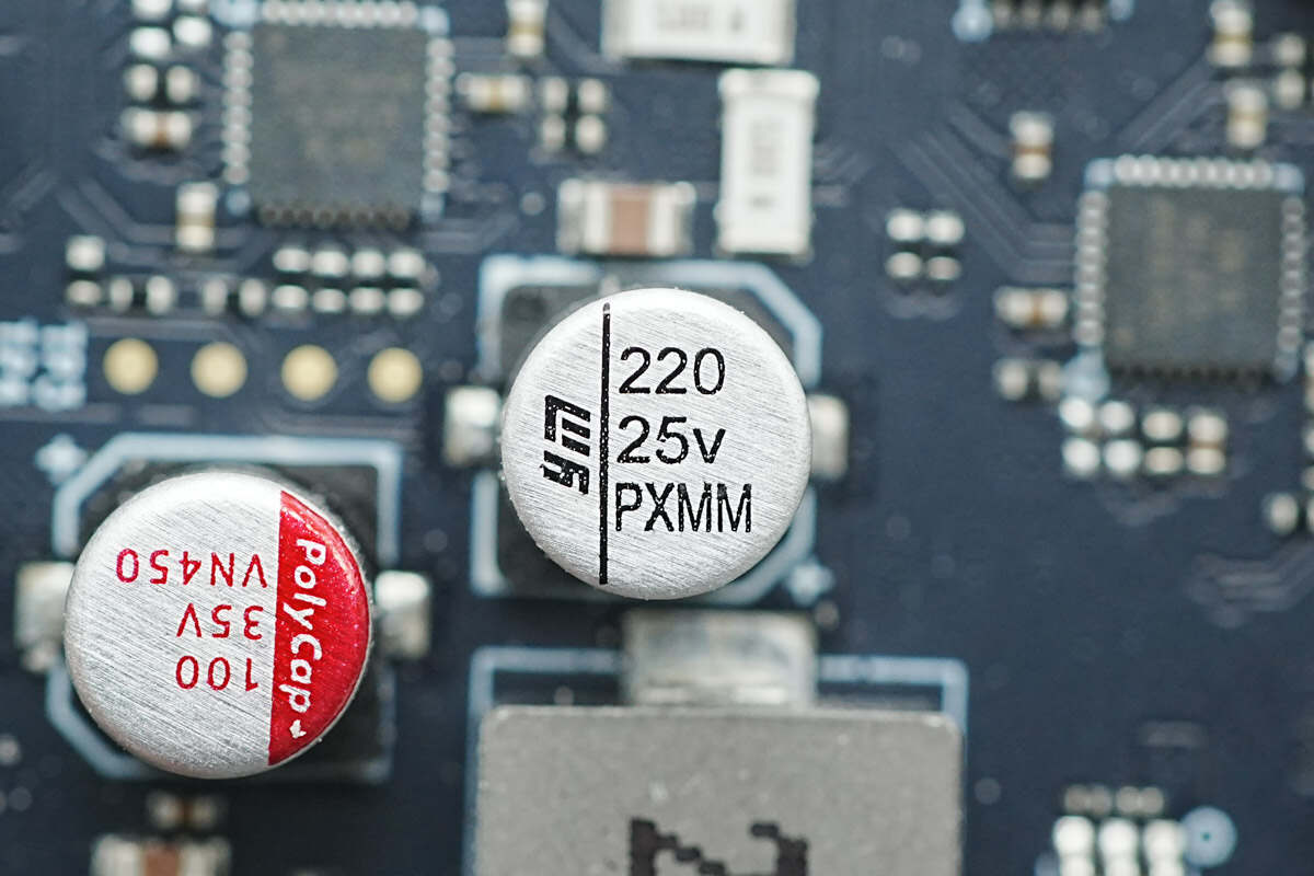
The capacitors for output filtering are from YMIN, VPX series solid-state chip capacitors. 220μF 25V.
The output VBUS MOSFET is from JSCJ and has the same model as the synchronous buck MOSFET.
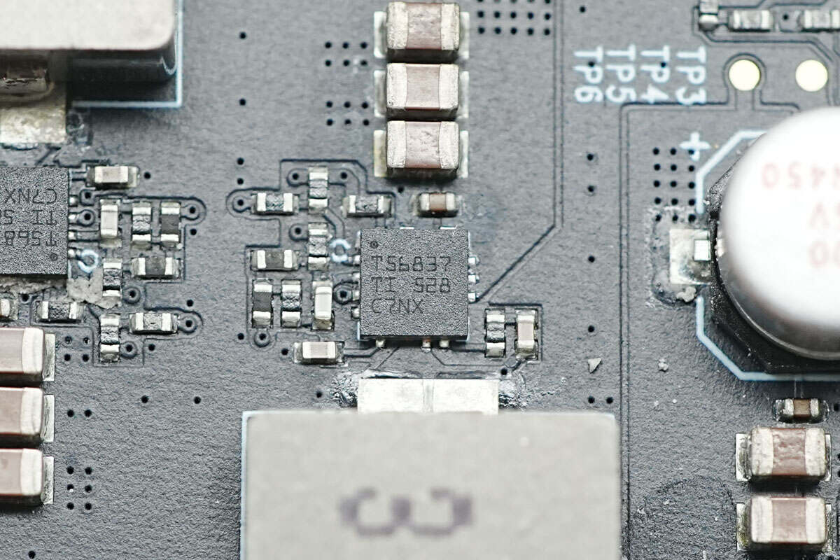
The synchronous buck chip marked with T56837 is from TI. It is a synchronous buck converter with a 28V input voltage and 8A output current. The chip integrates internal MOSFETs with on-resistances of 20.4mΩ and 9.5mΩ. It supports an output voltage range of 0.6V to 13V and features Eco-mode for improved light-load efficiency. The package type is QFN-10. Model is TPS56837
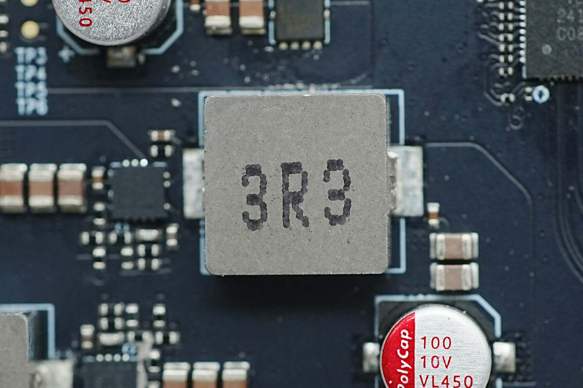
This is a 3.3μH alloy inductor.
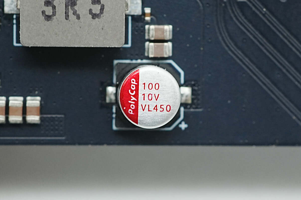
The filter capacitor is from PolyCap’s VL series, featuring long-life solid-state capacitors. 100μF 10V.
The two synchronous buck circuits are identical; to save space, only one is described here.
The synchronous buck chip is from Tollsemi. Model is TMI3410.
The synchronous buck chip marked with T5F is from Tollsemi. It supports a 5.5V input voltage, delivers 1.2A output current, operates at a switching frequency of 1.5MHz, and features input overvoltage protection, short-circuit protection, and over-temperature protection. It comes in an SOT23-5 package. Model is TMI3408F.
The overcurrent protection chip from ETA is used for overcurrent protection on the USB-A ports. Model is ETA6027.
The ETA6027 overcurrent protection chip is used for overcurrent protection on the USB-A ports.
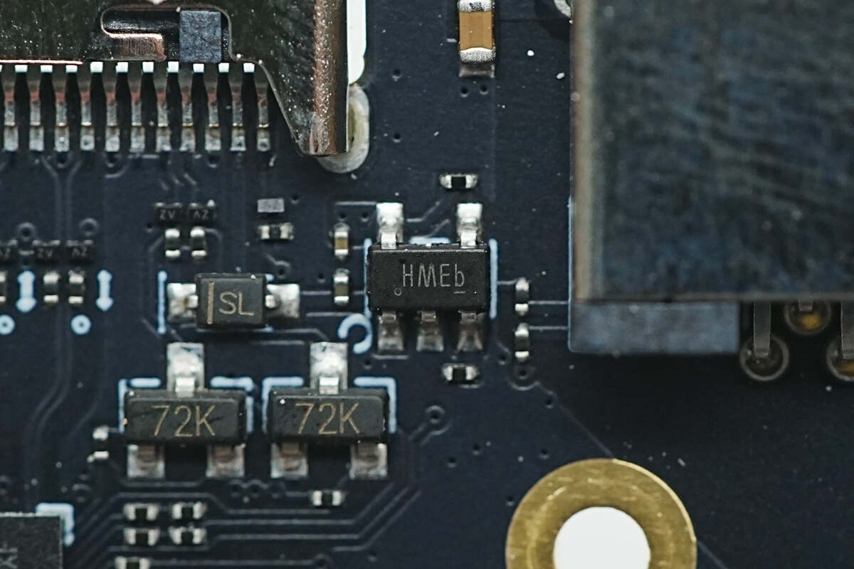
The HDMI port also uses the ETA6027 chip for overcurrent protection.
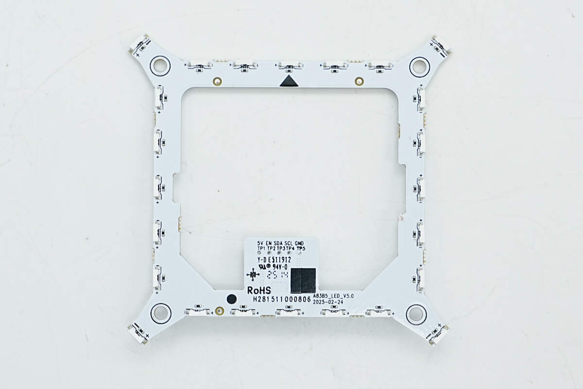
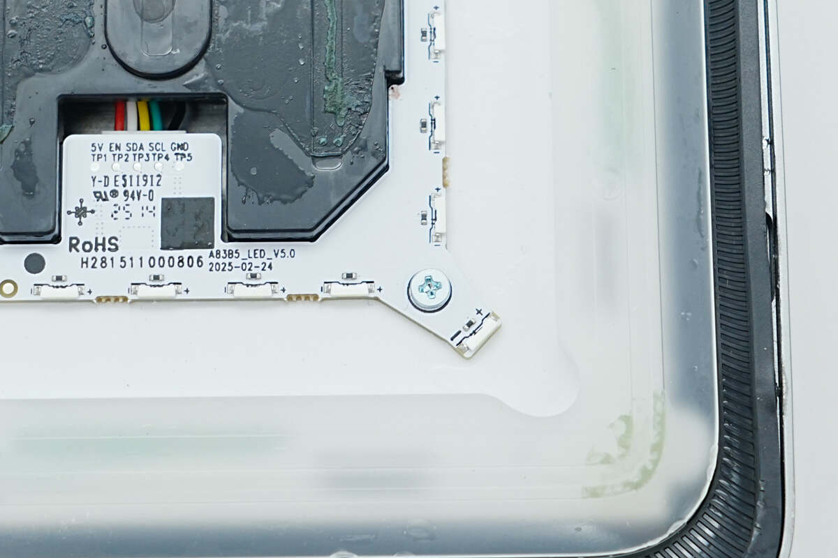
The LED board has 24 RGB LEDs.
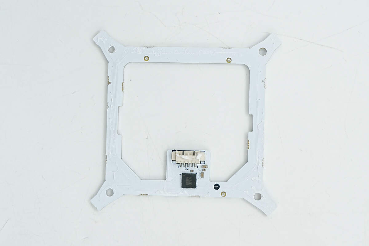
The back has a connector and a driver chip.
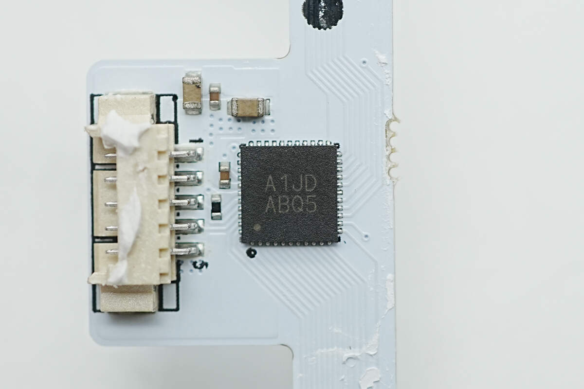
The LED driver marked with A1JD is from Awinnic. It features 36 LED driver channels and comes in a QFN 5×5-44L package. Model is AW21036QNR.
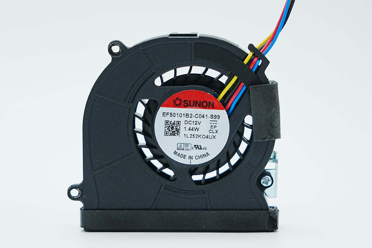
The cooling fan is from SUNON and is a centrifugal fan. 12V 1.44W. Model is EF50101B2.

Well, those are all components of the Anker Prime Thunderbolt 5 Dock (14-in-1, 8K).
Summary of ChargerLAB
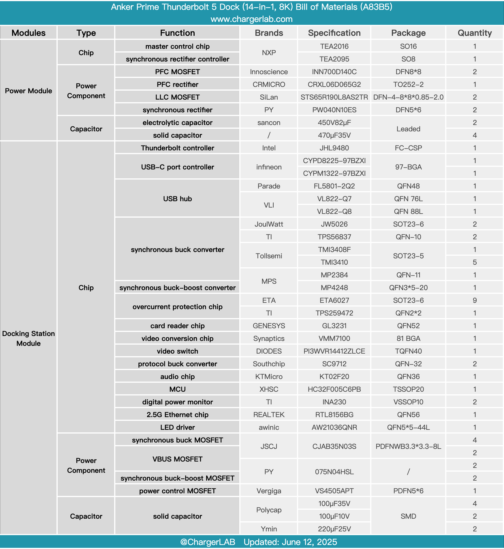
Here is the component list of the Anker Prime Thunderbolt 5 Dock (14-in-1, 8K) for your convenience.
After taking it apart, we found that it consists of two main sections: a GaN power module and a docking station module. The GaN power module is sealed in a plastic enclosure and filled with potting compound to enhance heat dissipation. Internally, it uses a combination of NXP’s TEA2016 and TEA2095 controllers, along with an Innoscience INN700D140C GaN FET and a CR MICRO CRXL06D065G2 SiC diode.
The docking station module consists of two PCBs—an upper and a lower PCB—connected via a high-speed connector. The Intel JHL9480 Thunderbolt controller handles Thunderbolt 5 port expansion. VIA Labs hub chips are used for USB port expansion, while the Synaptics VMM7100 converts DP signals to HDMI output. The SouthChip SC9712 is used for fast-charging output, and the MPS MP4248 handles synchronous buck-boost conversion. A cooling fan is built into the docking station to ensure stable and long-term operation.
Related Articles:
1. Teardown of MIIIW CB510 Pro 100W Two-in-One Supercharging Cable (iCB1013Y)
2. Teardown of Anker GaNPrime Lite 100W Charger (A121B)
3. Teardown of Original 60W PD Charger of Nintendo Switch 2