Introduction
Anker has released an ultra-thin magnetic portable charger with a thickness of approximately 8.7mm. It features a metal frame with rounded corners, and both sides are covered with skin-friendly materials for a more comfortable grip. The product houses a 5000mAh battery and supports 20W USB-C wired input and output, as well as 7.5W wireless output. Next, we will proceed with a teardown to examine its components and structure.
Product Appearance
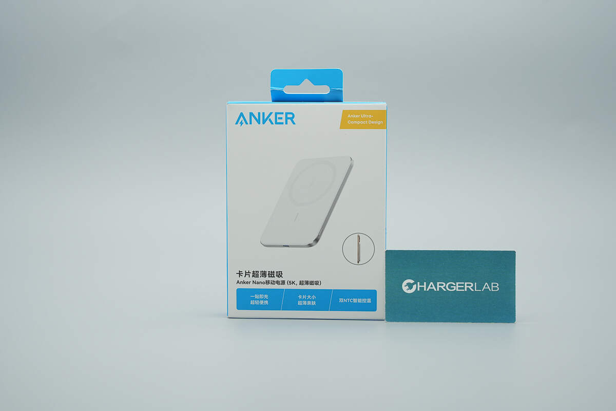
Front of the packaging features the Anker logo, product appearance, name, and selling points.
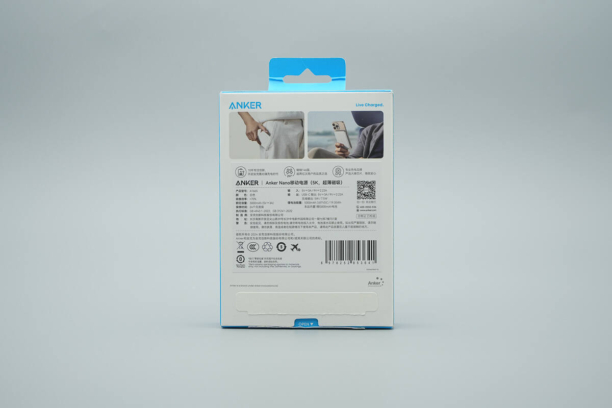
The back of the packaging displays selling points, specifications, precautions, and other relevant information.
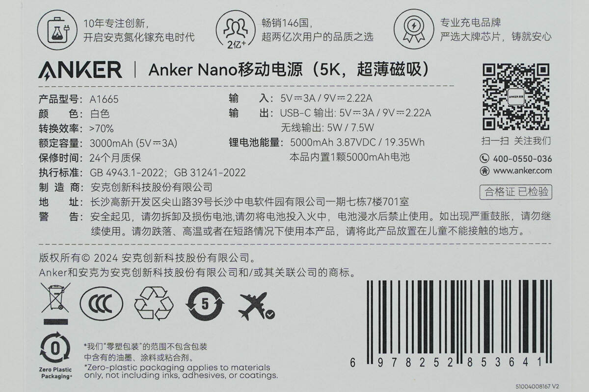
Product Model: A1665
Color: White
Warranty Period: 24 months
Standards Compliance: GB 4943.1-2022, GB 31241-2022
Rated Capacity: 3000mAh (5V3A)
Lithium Battery Energy: 5000mAh 3.87VDC / 19.35Wh
Built-in Battery: 1 × 5000mAh battery
Conversion Efficiency: >70%
Input: 5V3A / 9V2.22A
Wired Output (USB-C): 5V3A / 9V2.22A
Wireless Output: 5W / 7.5W
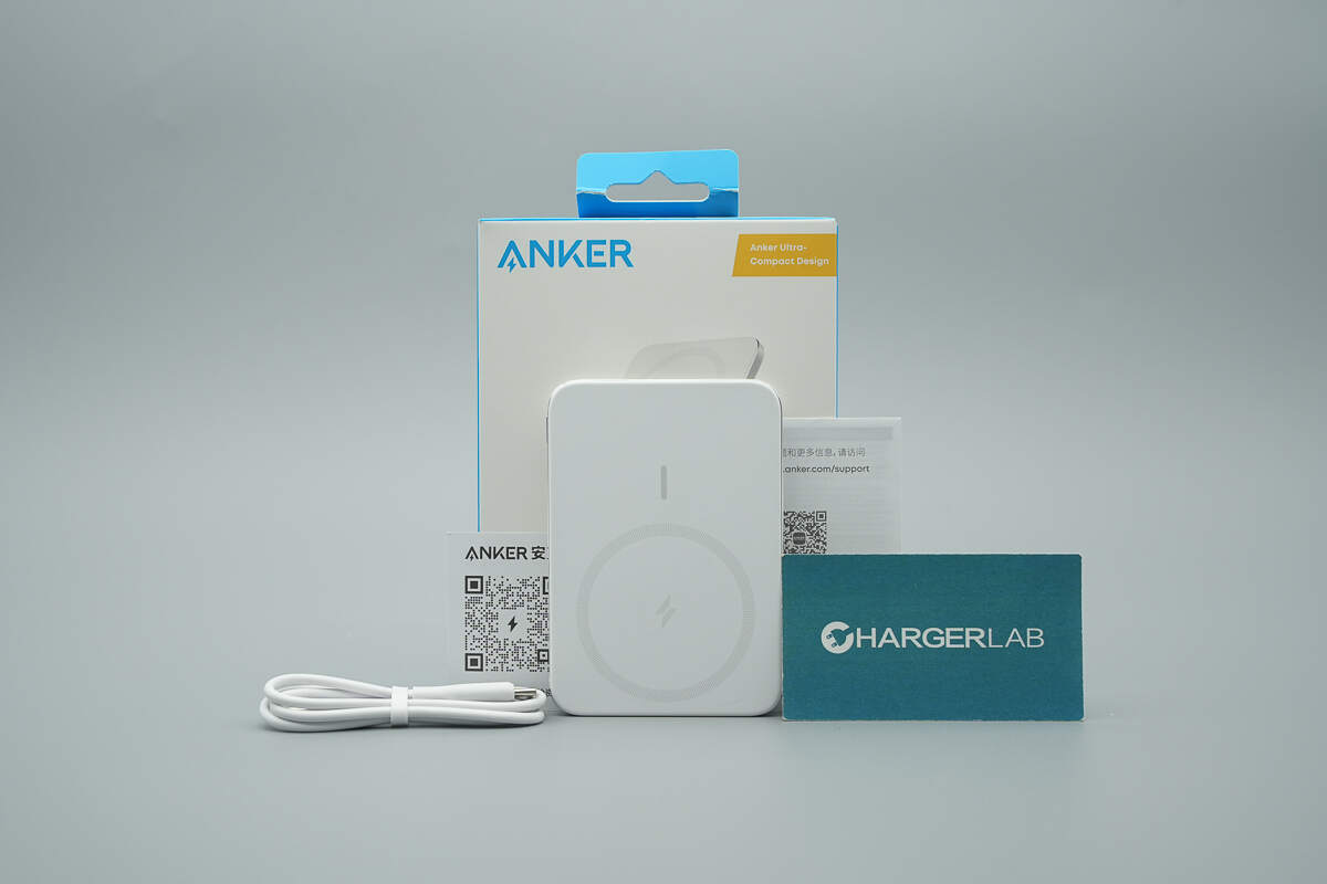
The package includes the power bank, a dual USB-C cable, and a user manual.
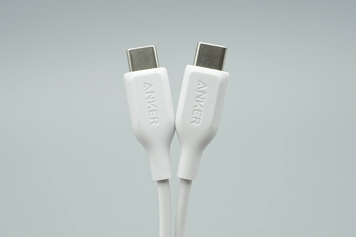
The included dual USB-C cable has ANKER printed on the connector ends.
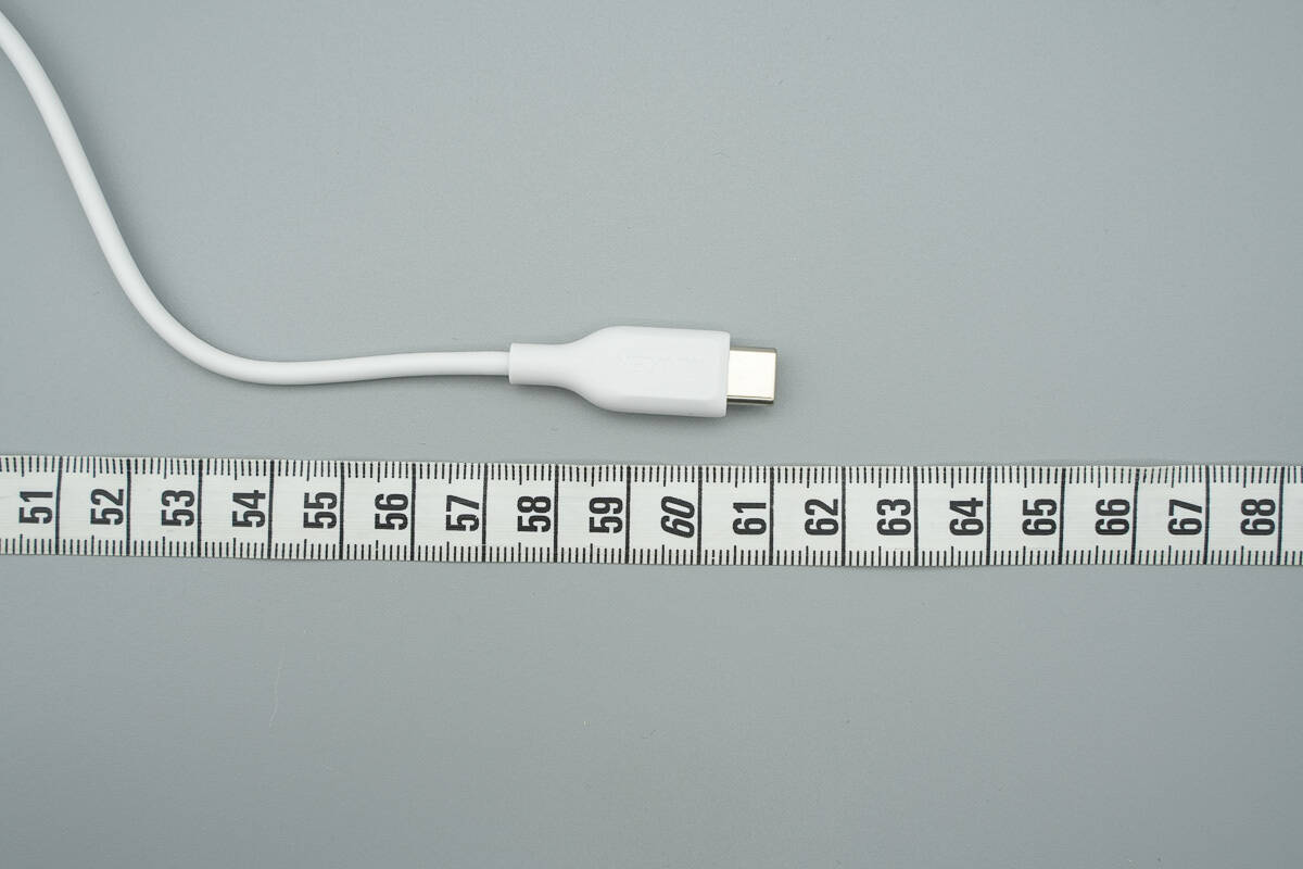
The length is about 61 cm (24.016 inches).
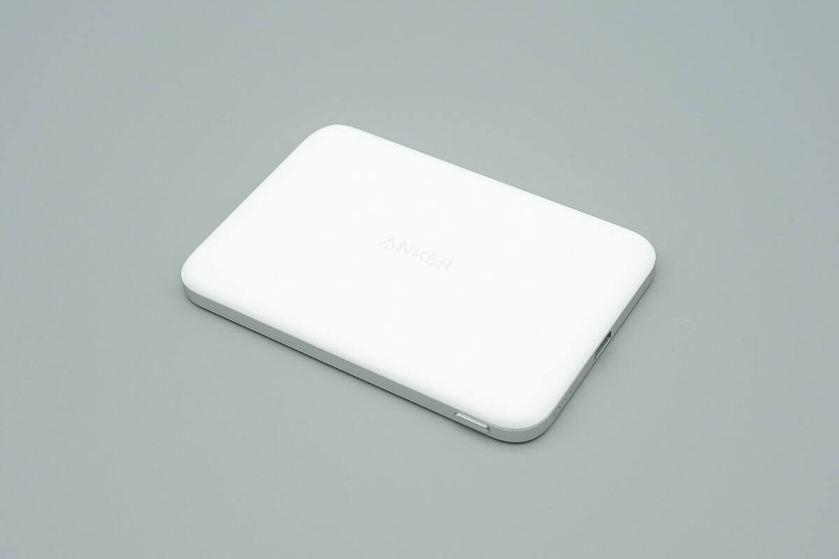
The body is extremely slim, with a metal frame and exquisite craftsmanship.
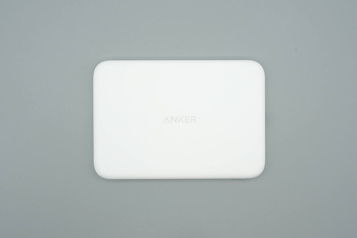
The front features the ANKER logo, with smoothly rounded corners.
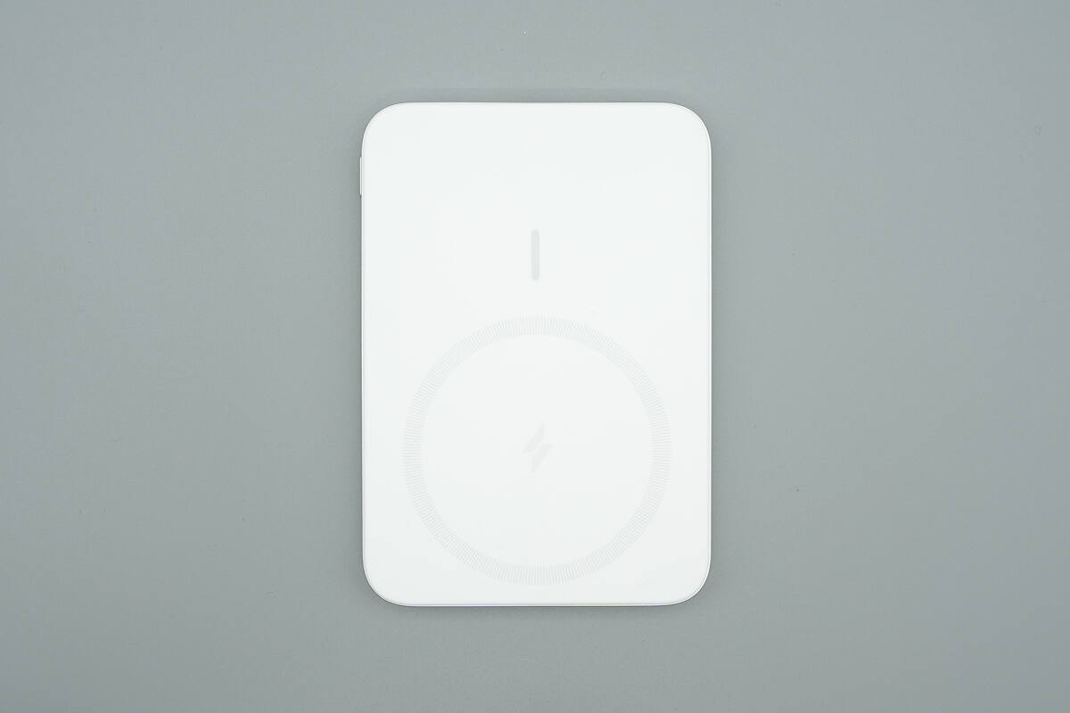
The magnetic surface also uses a skin-friendly material and is marked with a circular indicator for magnetic alignment.
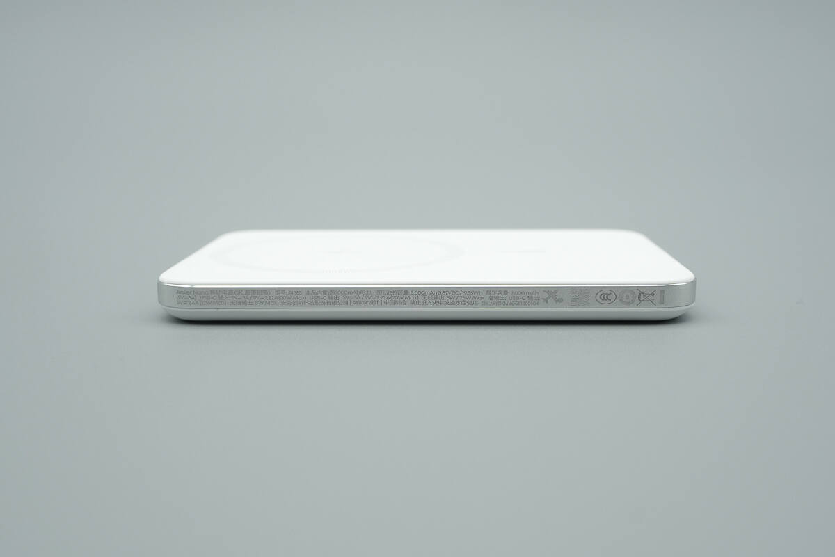
The frame is made of aluminum alloy, with product specifications and certification marks printed on the side.
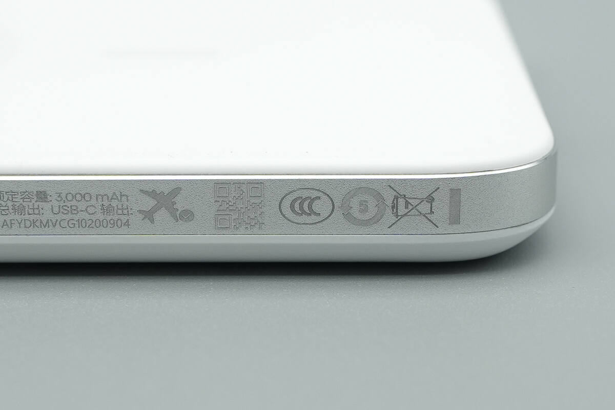
It has obtained 3C certification.
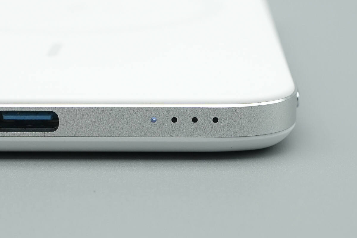
Close-up of the indicator lights.
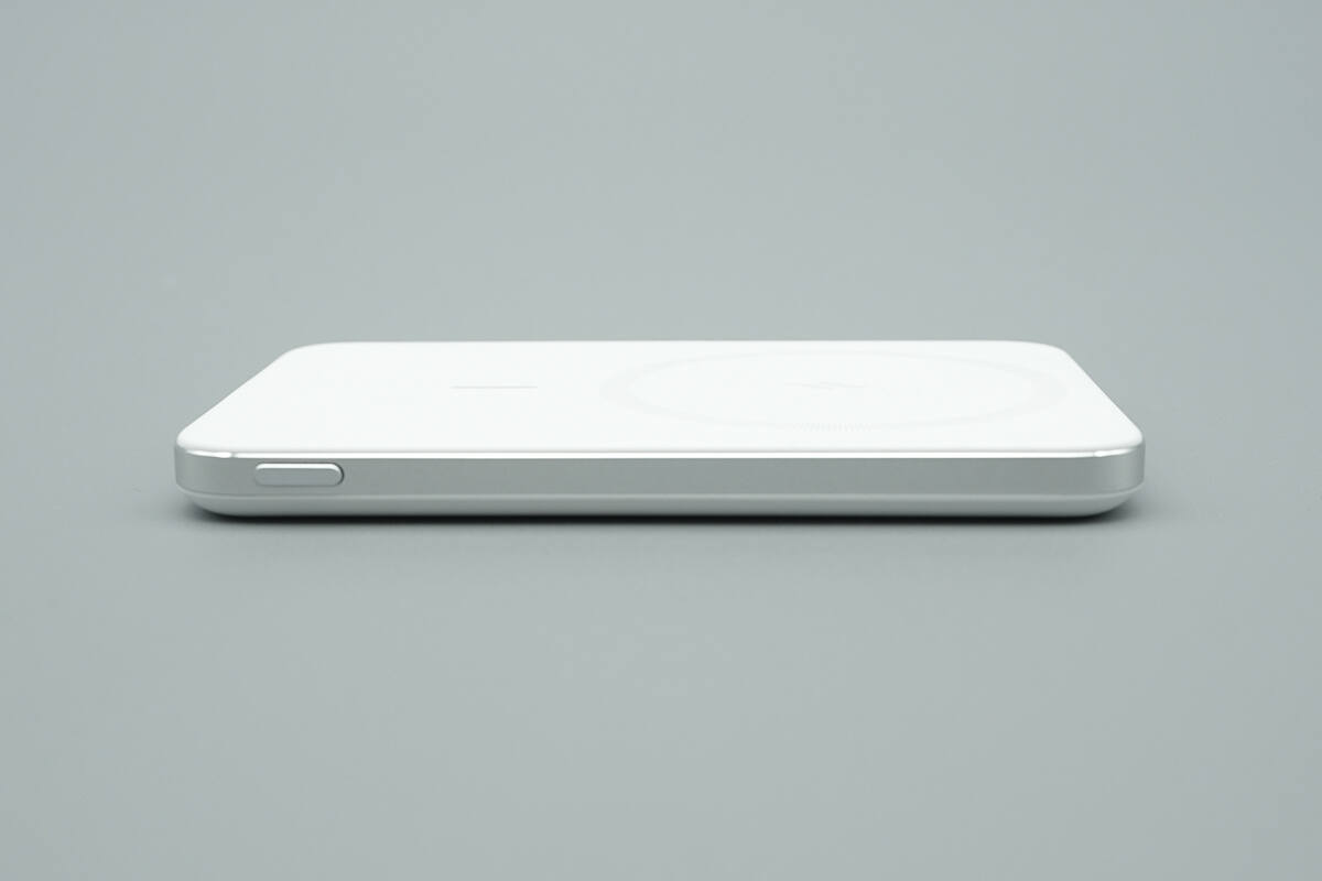
The other side features a power button.
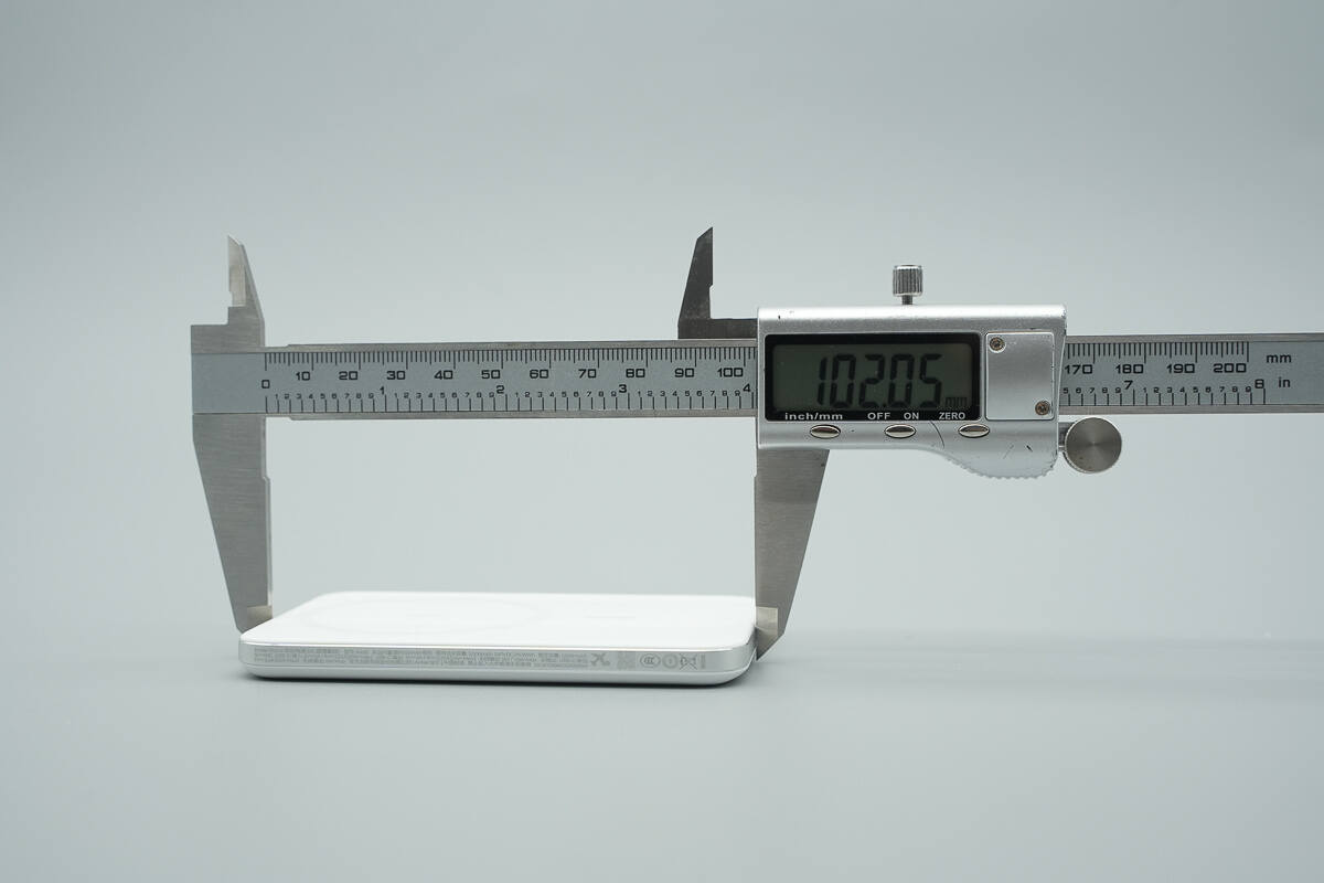
The length of the power bank is about 102.05 mm (4.018 inches).
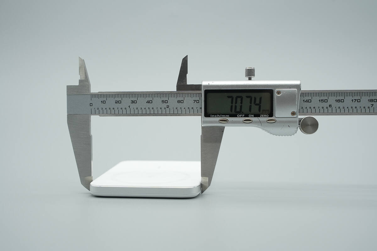
The width is about 70.74 mm (2.79 inches).
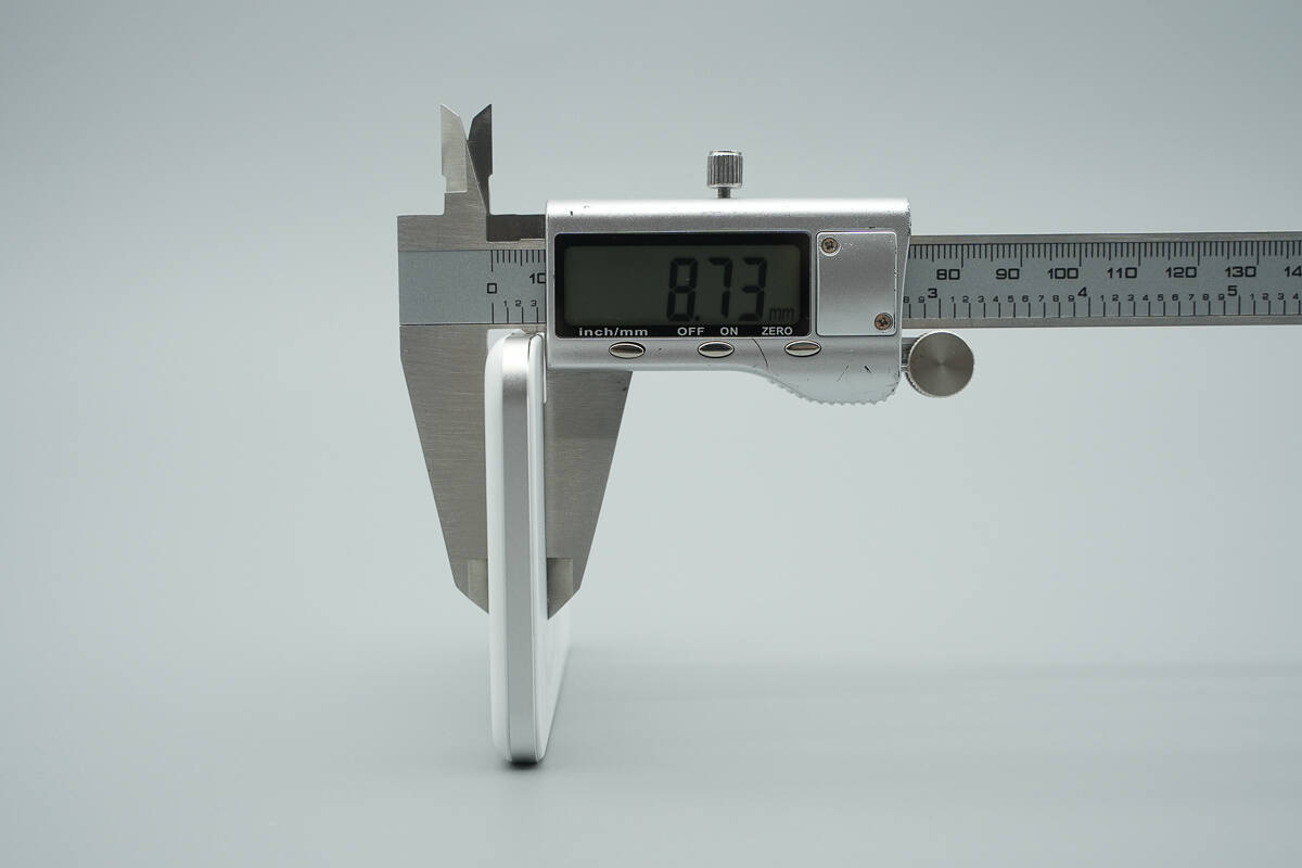
The thickness is about 8.73 mm (0.34 inches).
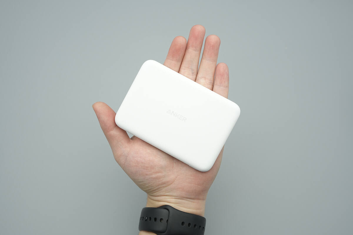
That's how big it is in the hand.
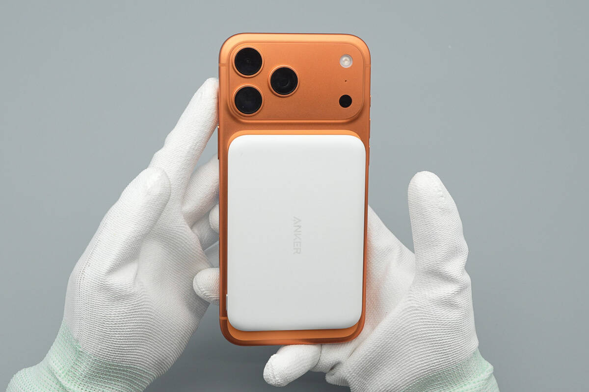
When wirelessly charging an iPhone 17 Pro Max, it does not obstruct the rear camera module.
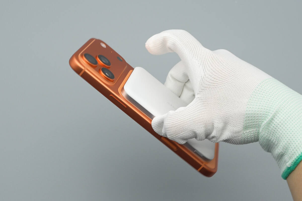
The power bank can securely hold the phone upside down without falling.
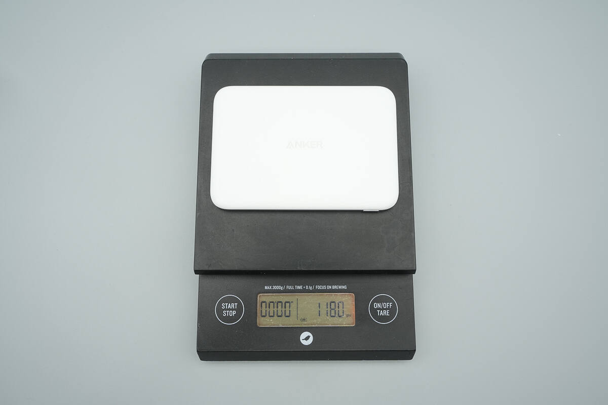
The weight is about 118 g (4.16 oz).
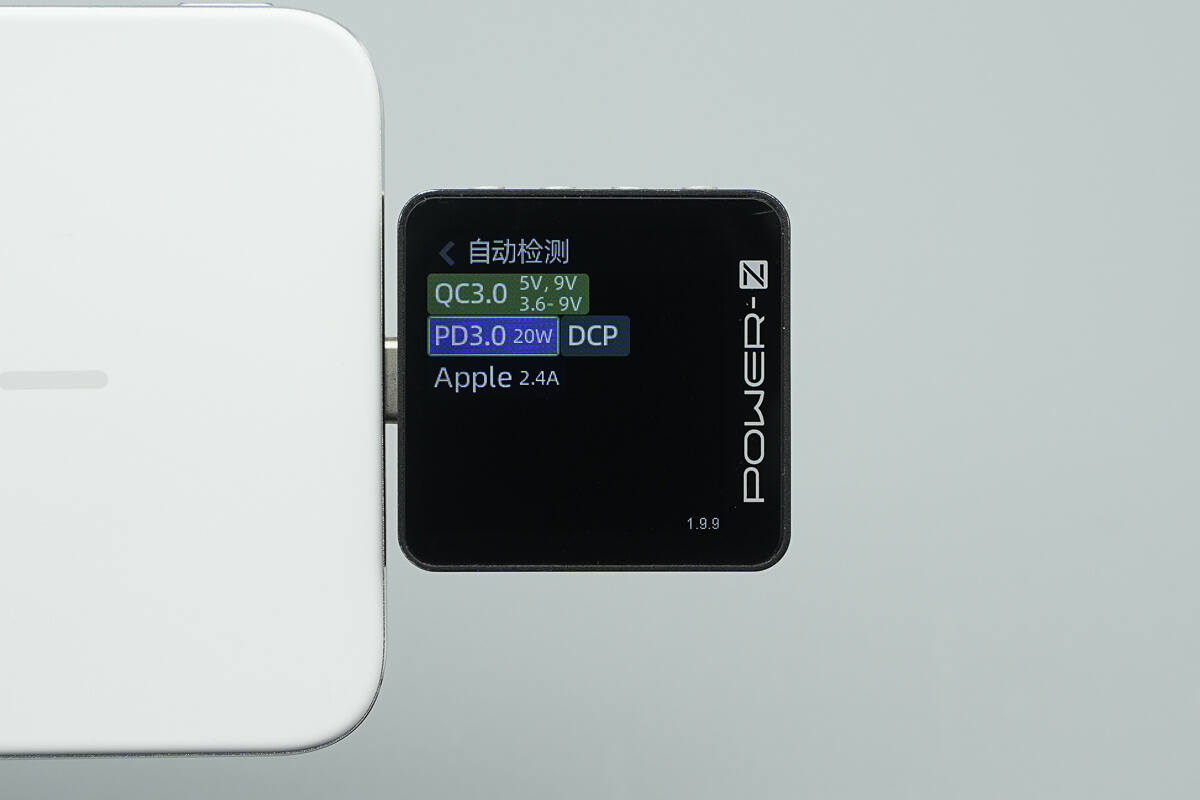
ChargerLAB POWER-Z KM003C shows that the USB-C port supports QC3.0, PD3.0, DCP, and Apple 2.4A charging protocols.
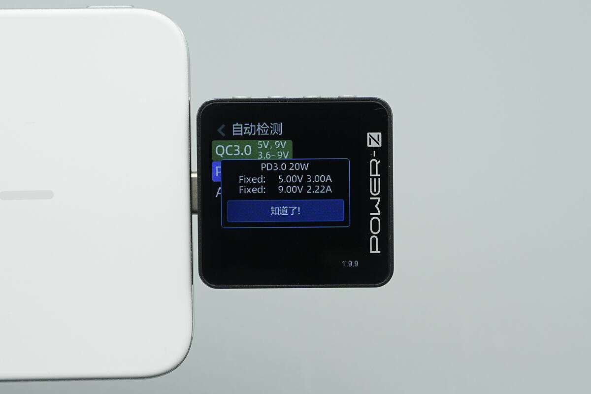
And it has two fixed PDOs of 5V3A and 9V2.22A.
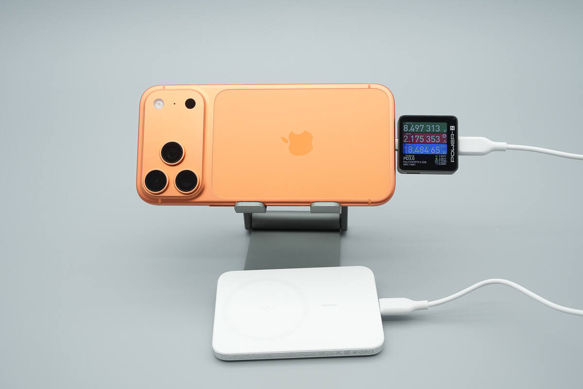
When charging the iPhone 17 Pro Max via USB-C, the power output is 18.48 W.
Teardown
Next, let's take it apart to see its internal components and structure.
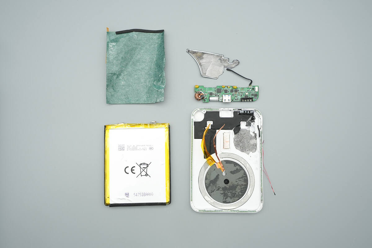
Remove the casing.
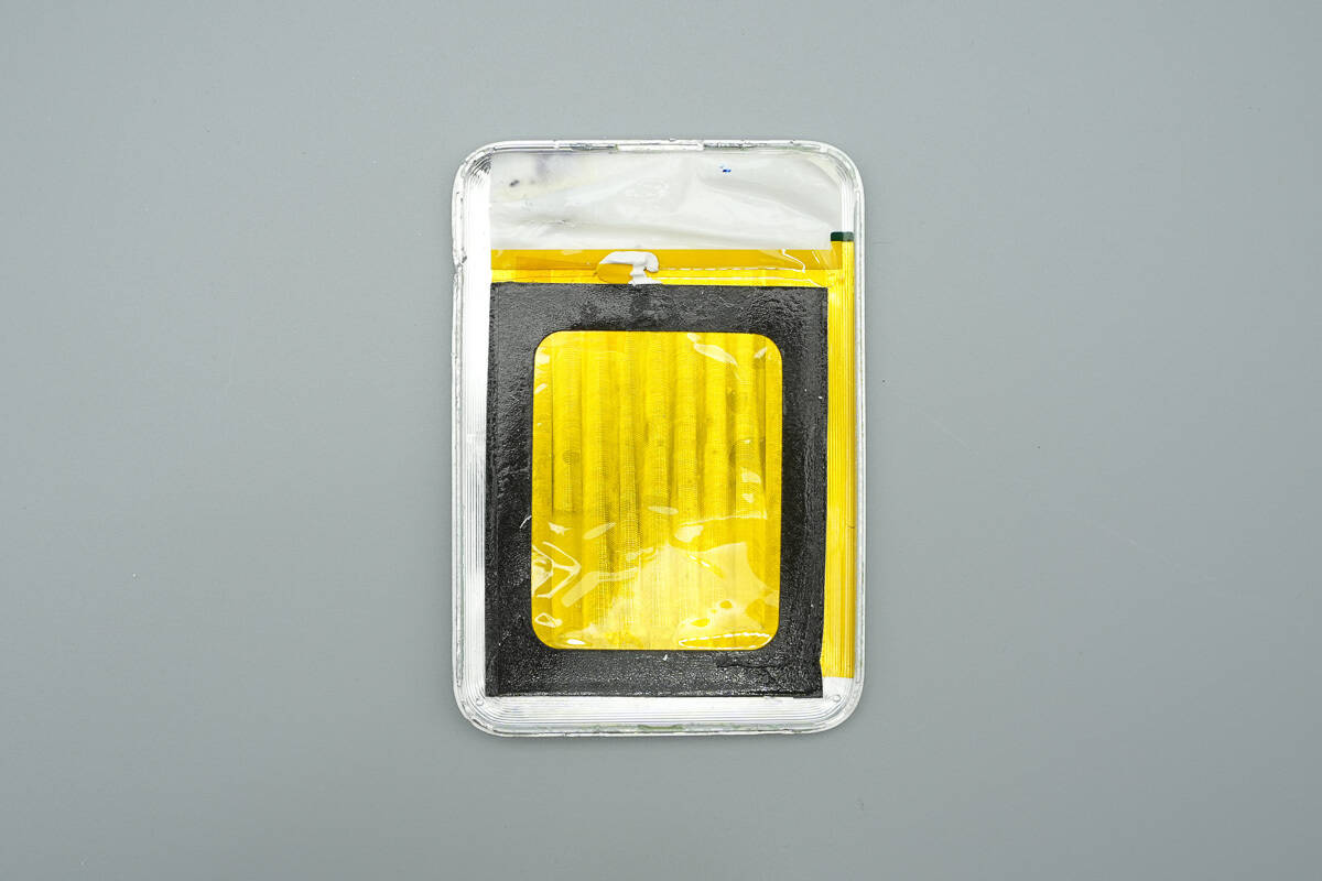
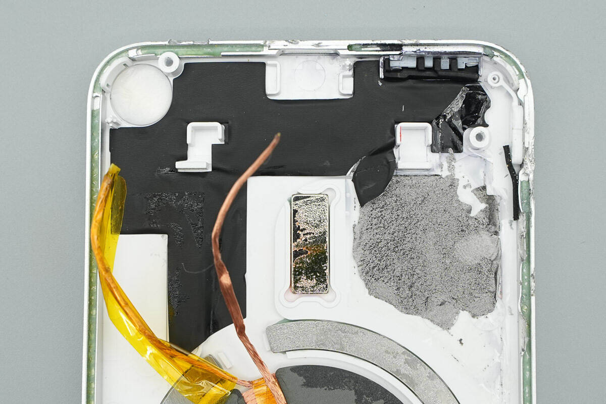
A white film is applied on the inner side of the casing in areas corresponding to the PCB for insulation and heat resistance. In areas corresponding to the battery cells, a yellow high-temperature insulating tape is applied, along with black foam sealing adhesive.
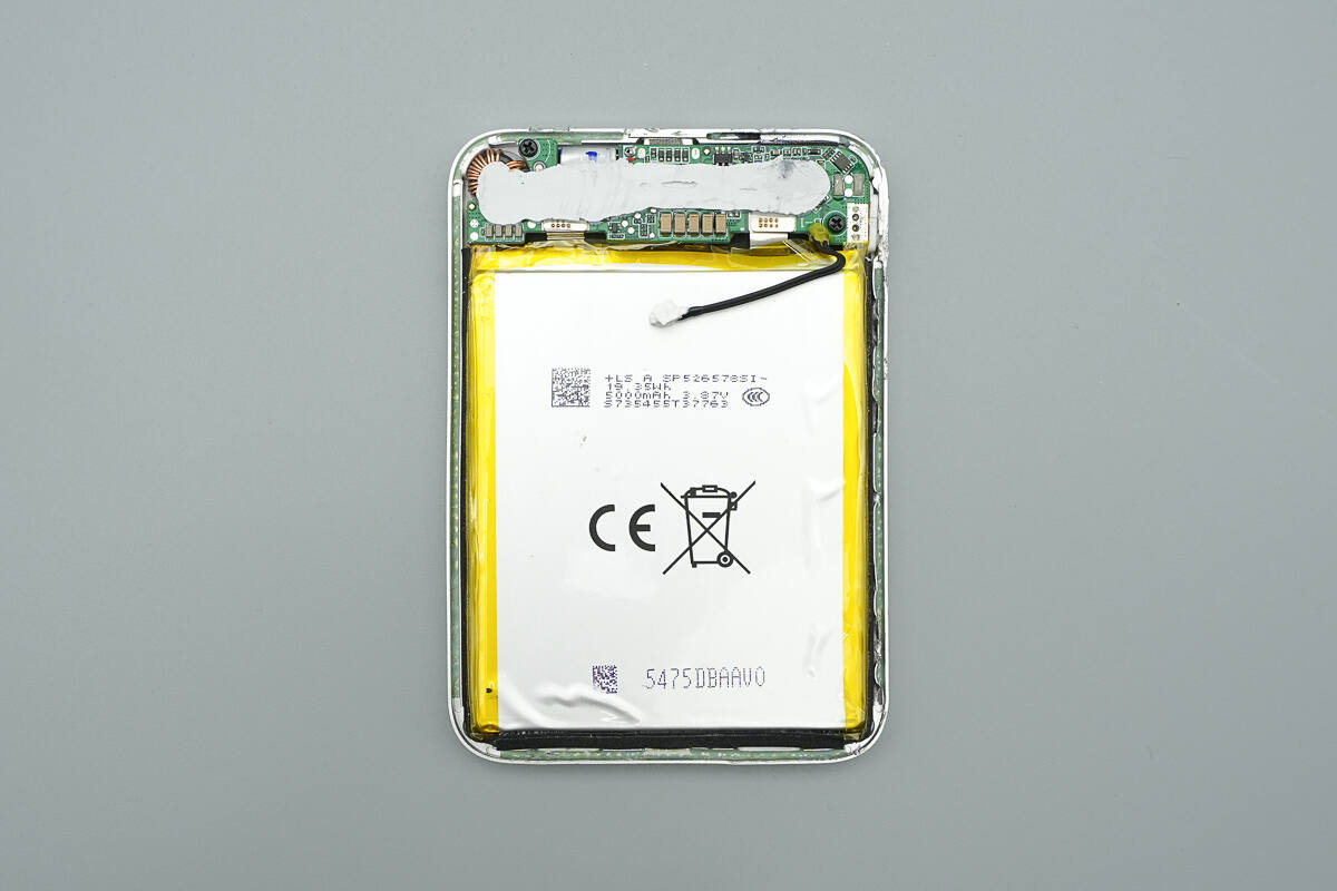
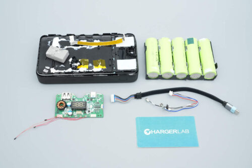
The top section houses the PCBA module, while the lower section contains the battery pack.
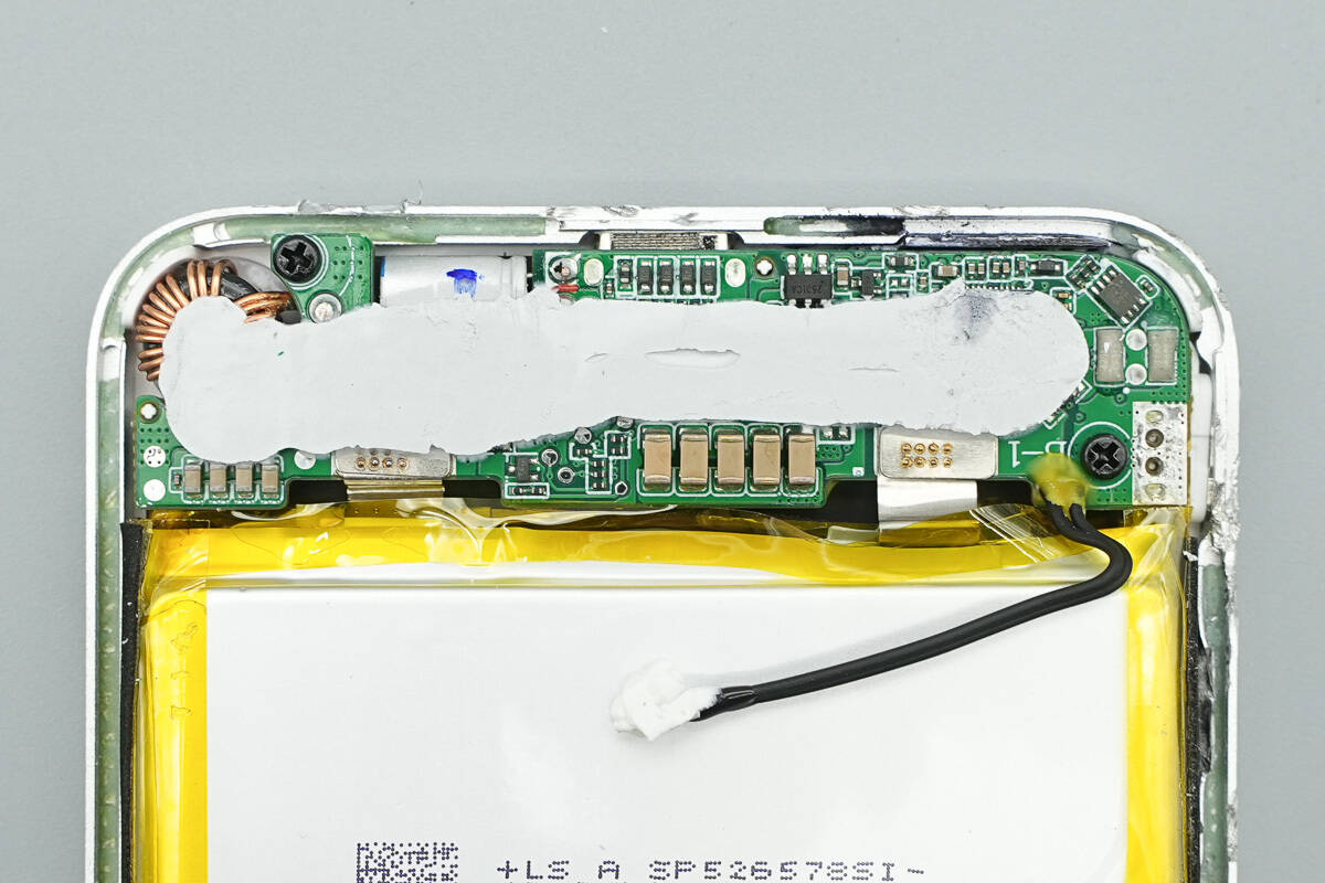
The NTC thermistor is secured onto the battery cell with white adhesive.
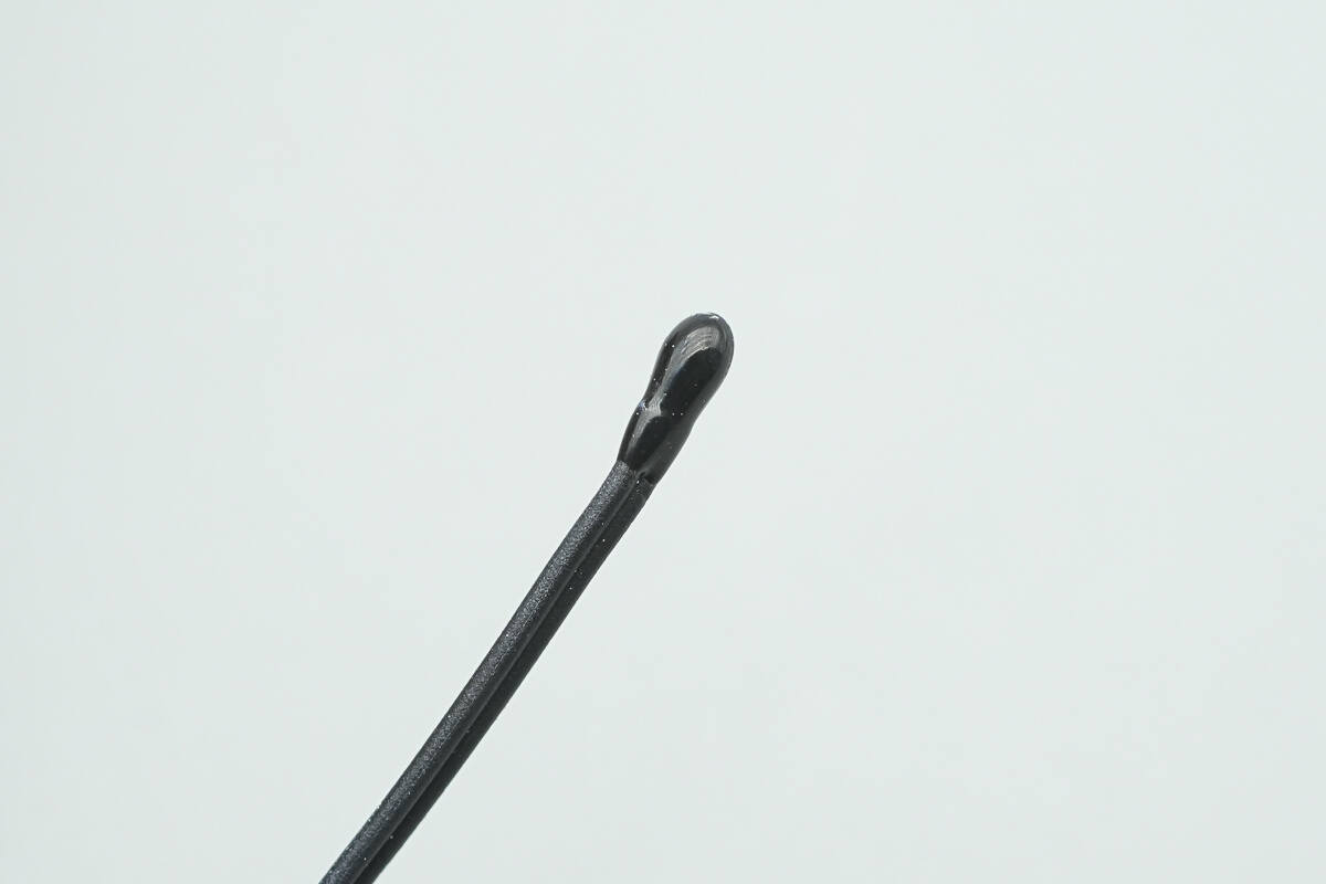
Close-up of the NTC thermistor.
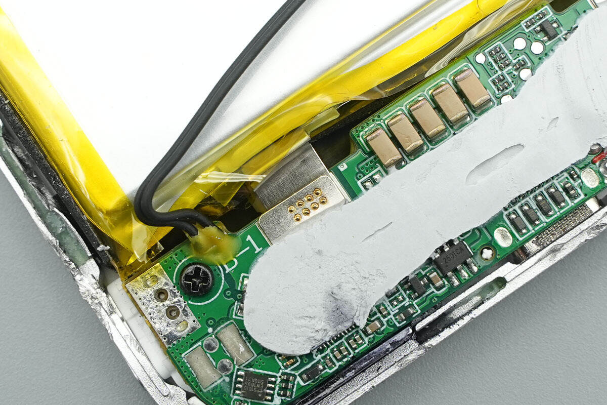
The PCB is secured with screws, and the battery is connected to the PCB via nickel strip spot welding.
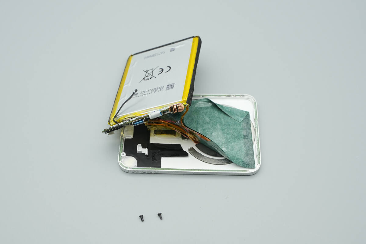
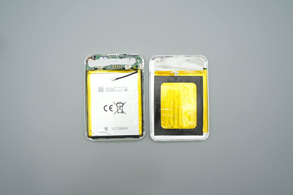
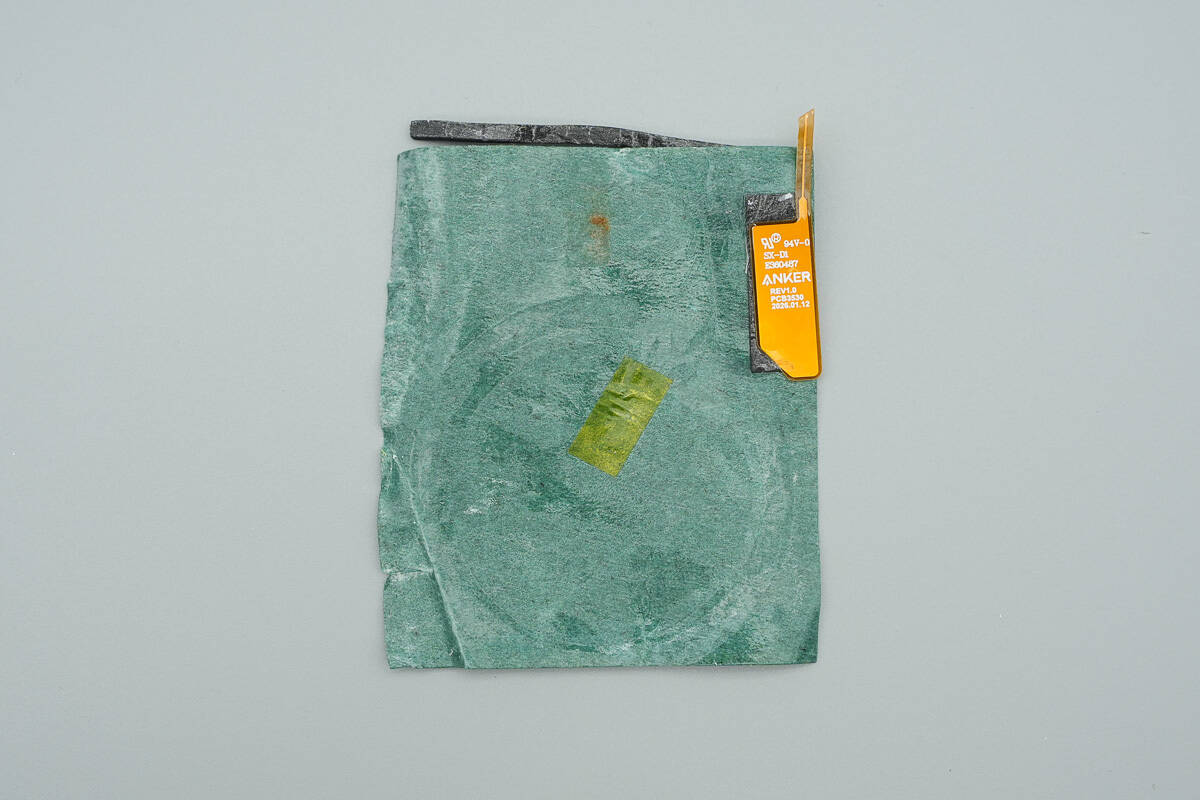
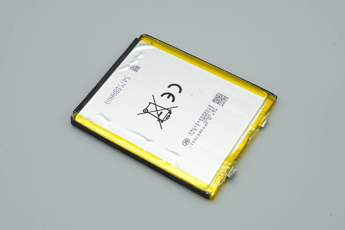
Remove the battery pack and PCB. The space between the battery cells and the casing is insulated with kraft paper.
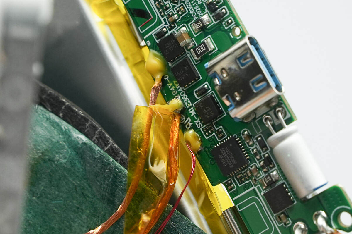
The wireless charging coil and the thermistor are both soldered onto the PCB.
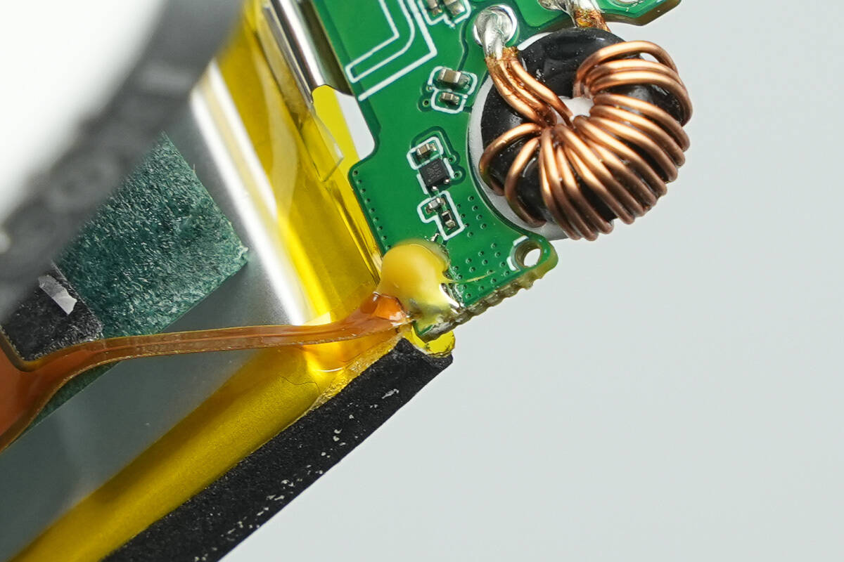
The welding points of the electrode tabs are also reinforced with yellow adhesive.
Separate the battery cell from the PCB.
There is an electrode pad on the kraft paper used to detect the alignment between the power bank and the phone.
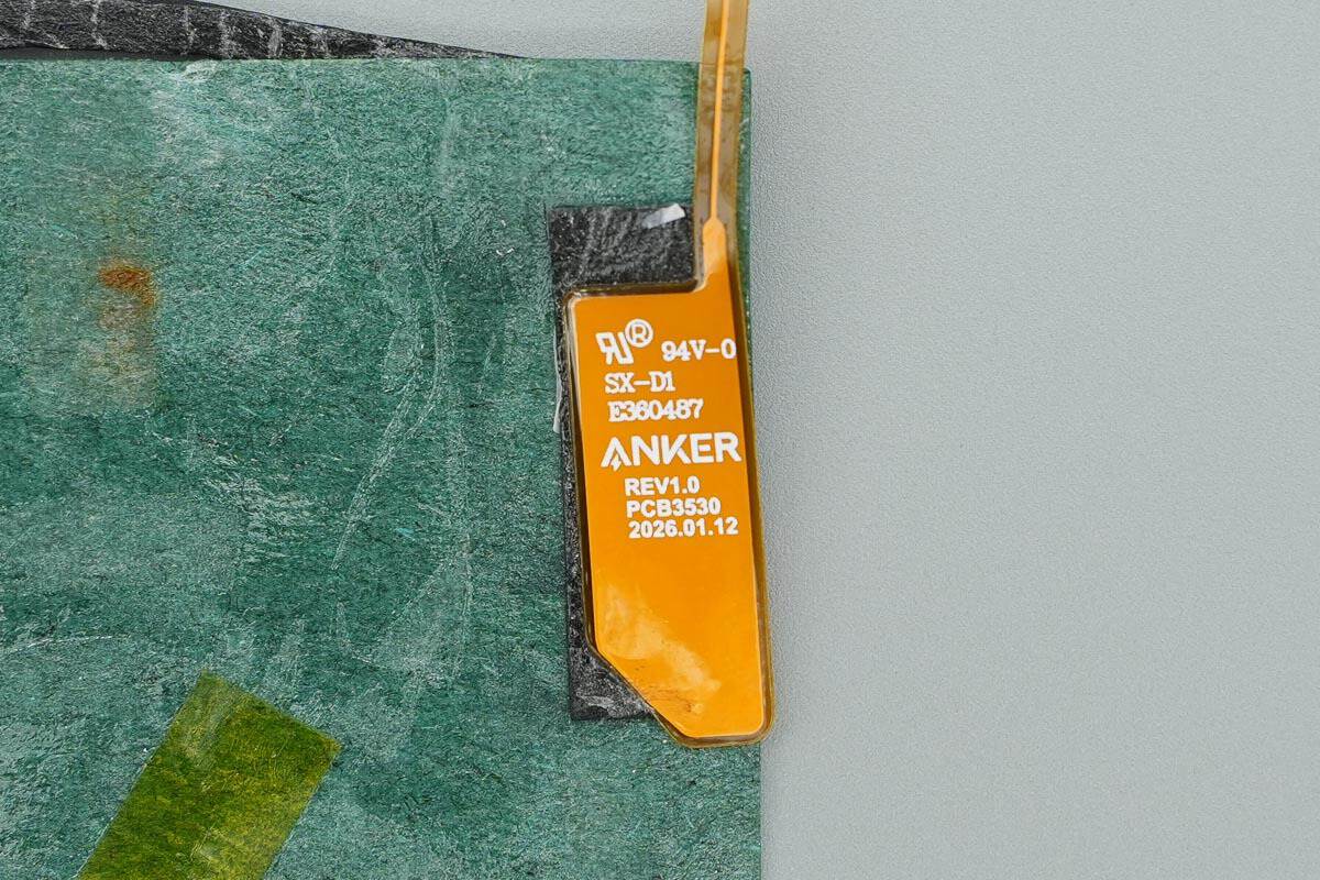
The electrode pad is sourced from Anker.
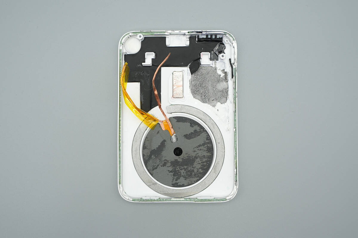
Interior view of the casing.
A graphene heat dissipation sheet is installed in the top section corresponding to the PCB.
Black cushioning foam is applied around all sides of the battery.
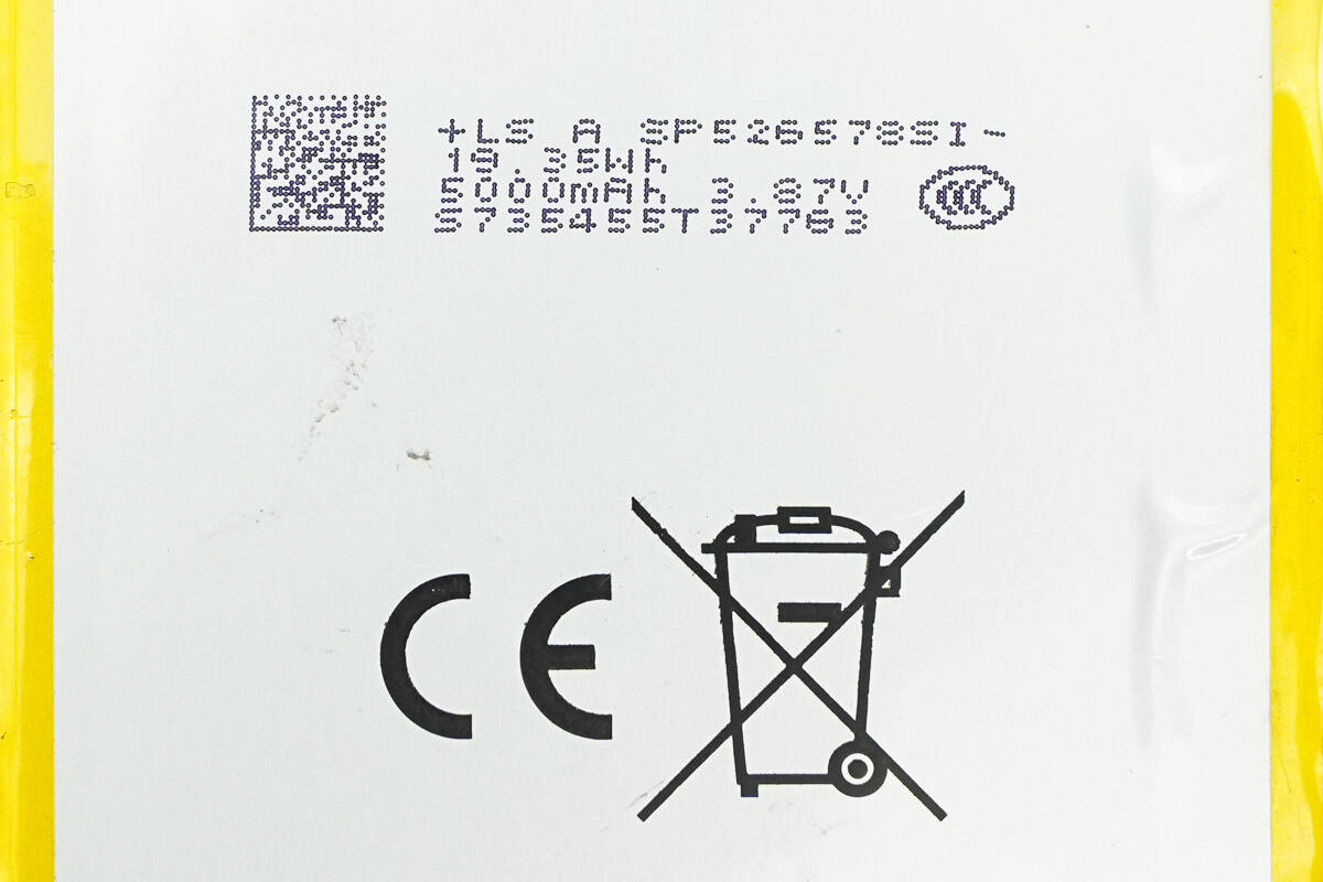
The battery is from LS, model SP526578SI, with a rated voltage of 3.87 V, a capacity of 5000 mAh, and an energy of 19.35 Wh. It has passed the CCC certification.
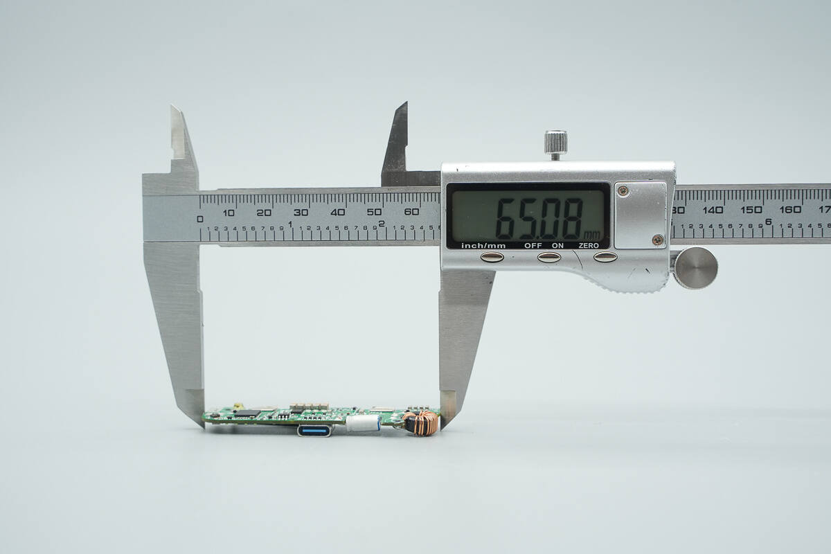
The length of the PCB is about 65.08 mm (2.56 inches).
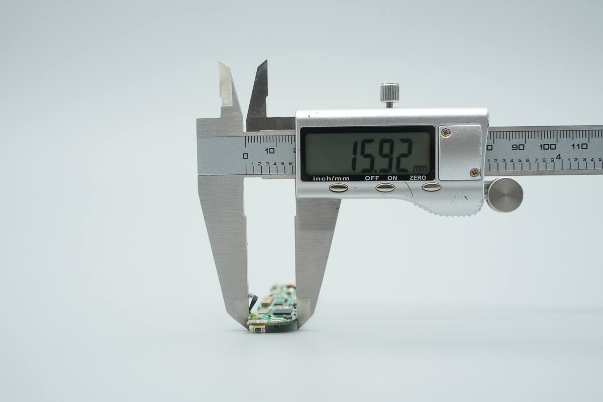
The width is about 15.92 mm (0.63 inches).
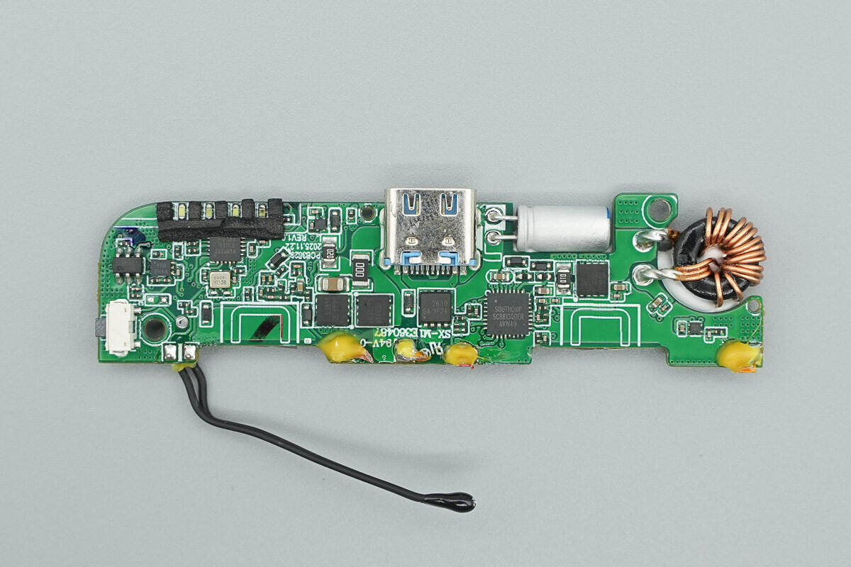
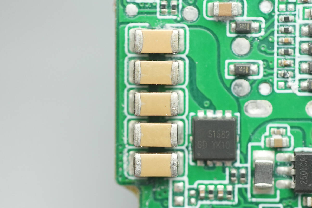
The front side of the PCB features a battery protection chip, battery protection MOSFETs, wireless charging power MOSFETs, a VBUS MOSFET, as well as filtering capacitors and other components.
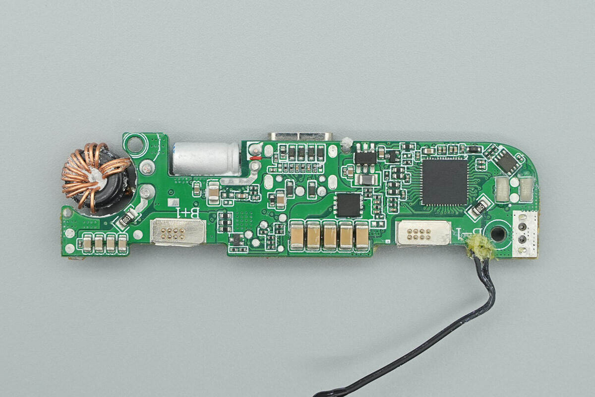
The back side of the PCB is equipped with a wireless charging master control chip, an authentication chip, a switching MOSFET, NPO resonant capacitors, and other components.
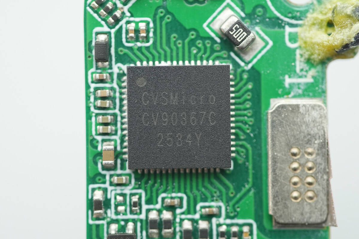
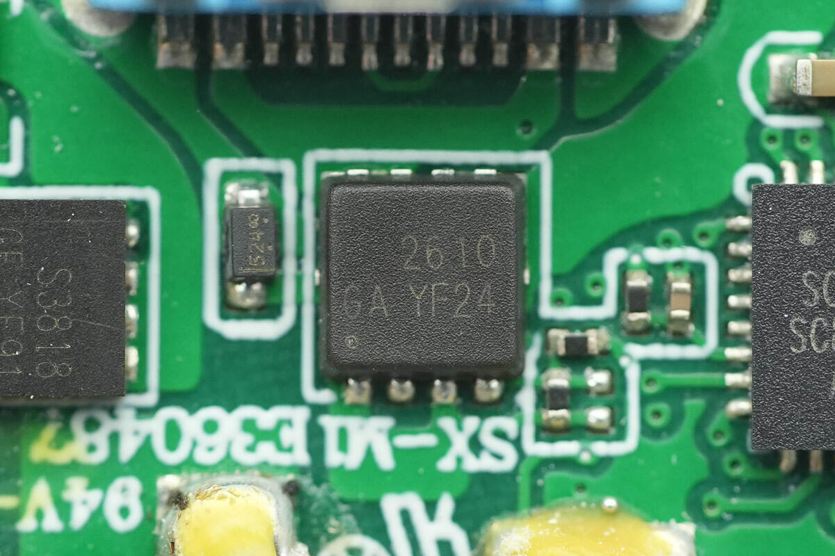
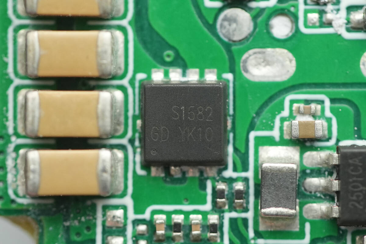
The wireless charging and power bank master control chip is sourced from CVS, model CV90367C. It is a low-quiescent-current SoC supporting Qi 2.0 and Qi 2.2 wireless charging standards.
The chip integrates USB-C port control, wireless charging control, and pre-driver modules. It supports Q-factor detection, communication decoding, and FOD (Foreign Object Detection), and is compatible with wireless charging standards including 5 W BPP, 7.5 W Apple MagSafe, and 15 W EPP. It is suitable for magnetic wireless charging power banks and similar products.
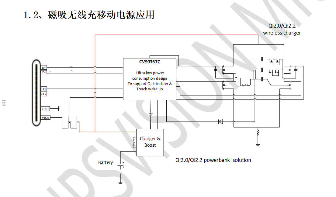
The CV90367C also integrates a bidirectional full-featured Type-C controller, supporting multiple fast-charging protocols including UFCS, PPS, PD, SCP, FCP, QC, AFC, and BC1.2. It features ultra-low standby power consumption and multiple protection mechanisms, including input over-voltage/under-voltage, over-current, short-circuit, and over-temperature protection. This enhances system integration while ensuring both low power consumption and safety. The chip comes in a QFN56 package.
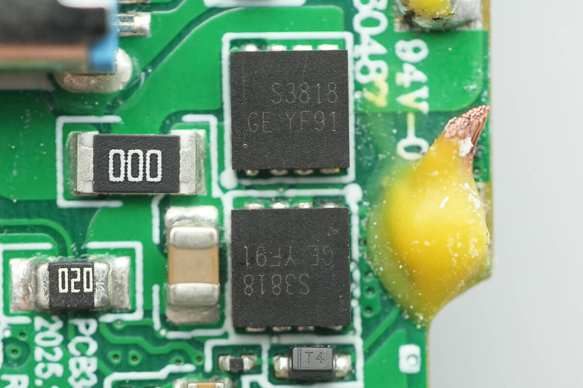
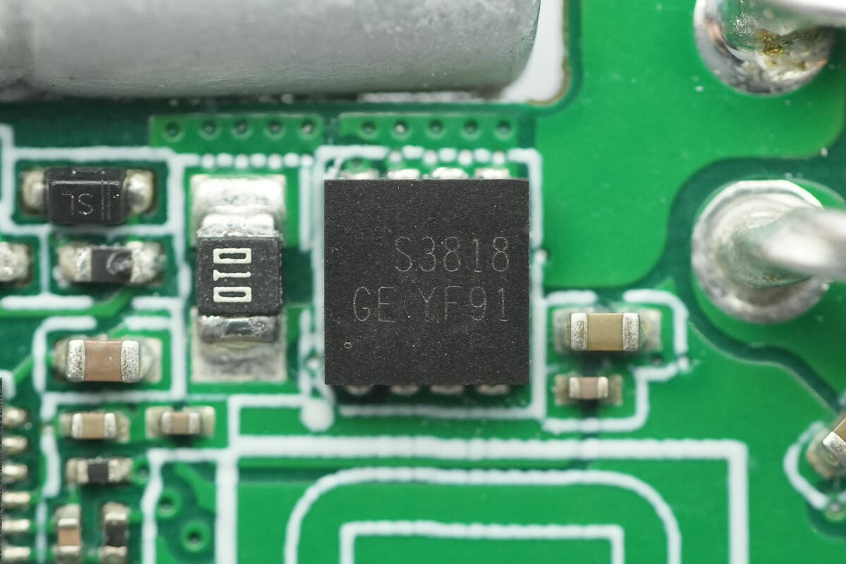
The two wireless charging power MOSFETs are sourced from Leadteck, model LTS3818FRDY. They are dual-channel asymmetric NMOS transistors with a voltage rating of 30 V and an on-resistance of 3.5 mΩ, packaged in a TDFN 3×3-8L package.
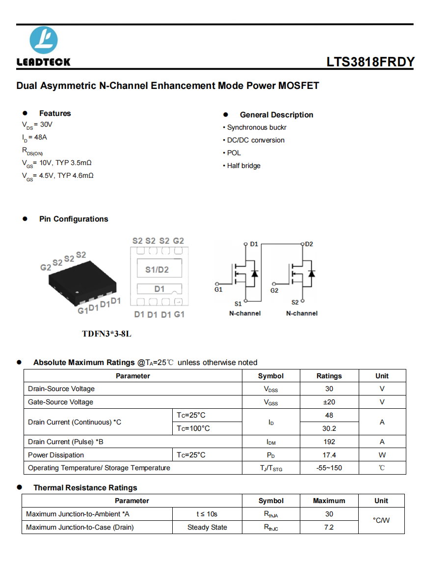
Here is the information about LTS3818FRDY.
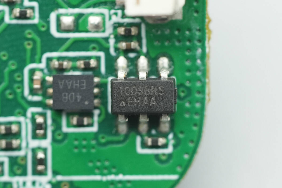
The battery protection chip is an iCM CM1003-BNS, a protection IC designed for single-cell rechargeable lithium batteries. It features a high-precision voltage detection circuit and a delay circuit, enabling protection against overcharge, over-discharge, and overcurrent by monitoring the battery’s voltage and current. It is suitable for protection circuits of single-cell lithium-ion or lithium-polymer rechargeable batteries.
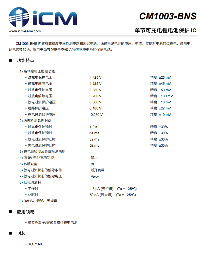
Here is the information about iCM CM1003-BNS.
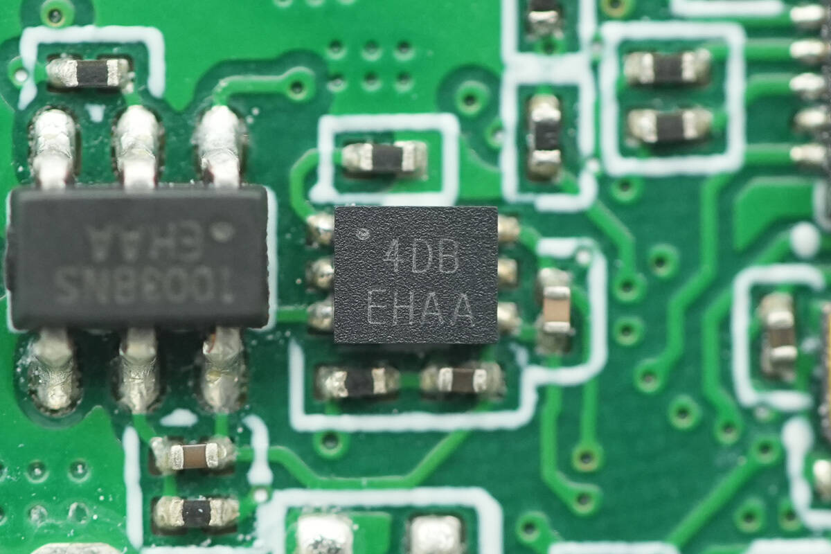
Next to it is an iCM CM1004-DBD, marked with “4DB.” This single-cell battery protection IC supports an external current-sensing resistor and provides higher-precision overcurrent detection. Together with the CM1003-BNS, it forms a dual-layer battery protection scheme.
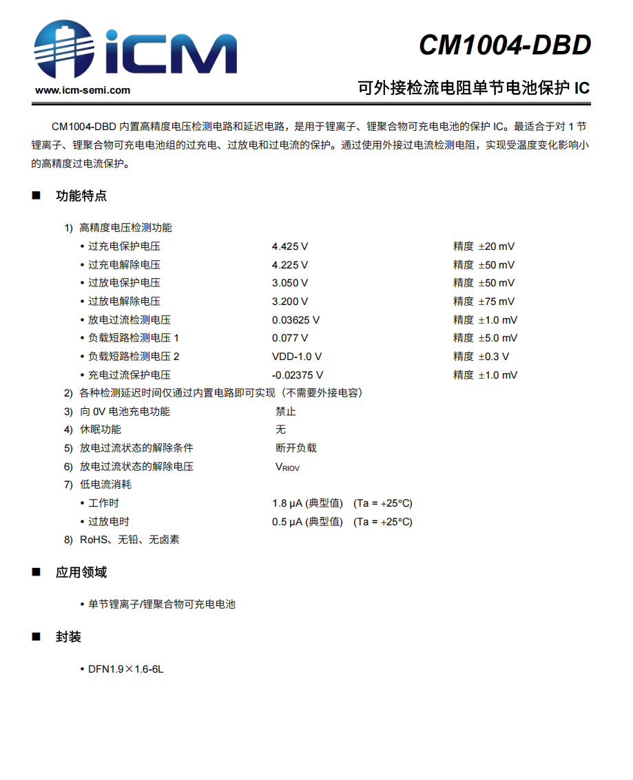
Here is the information about iCM CM1004-DBD.
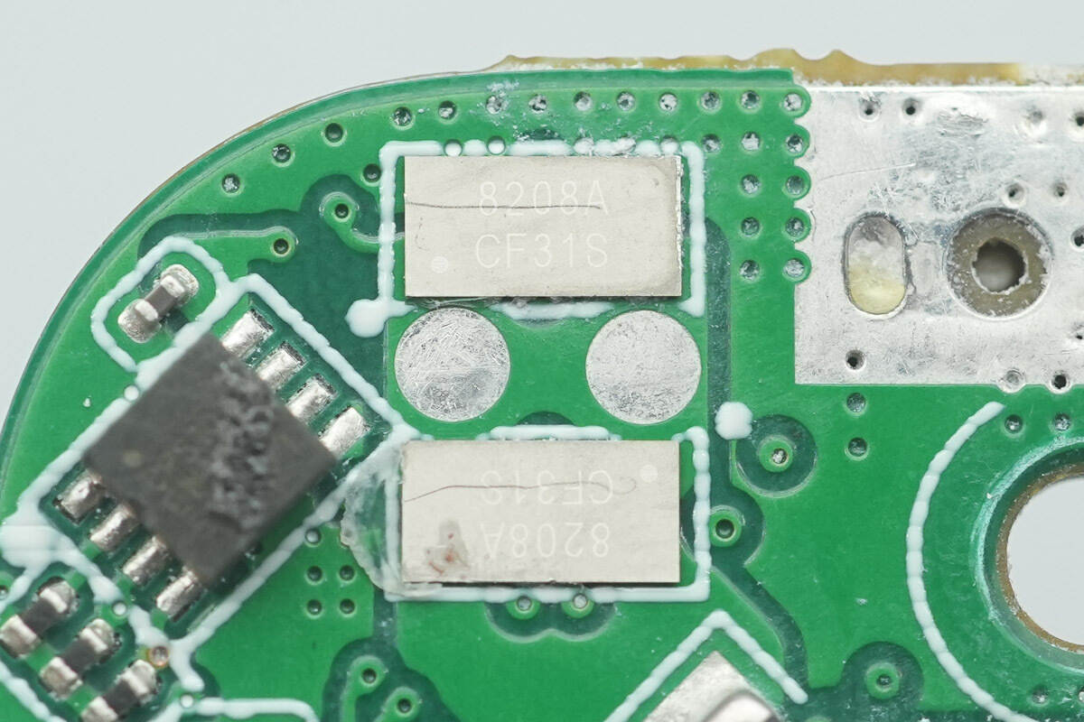
The two battery protection MOSFETs are sourced from JSCJ, marked “8208A,” model CS8208SP-A. They are dual NMOS transistors with a voltage rating of 12 V and an on-resistance of 2.1 mΩ, packaged in a CSPC3015-10 package.
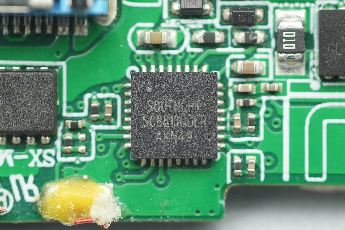
The charge–discharge controller is sourced from SouthChip, model SC8813. It is a synchronous buck charging controller that also supports reverse boost output and features an I²C interface. The switching frequency is adjustable, and it integrates a 10-bit ADC and charge indication. It supports a very wide input voltage range and is suitable for applications with 1–4 lithium cells.
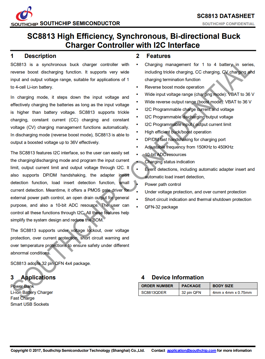
Here is the information about SouthChip SC8813.
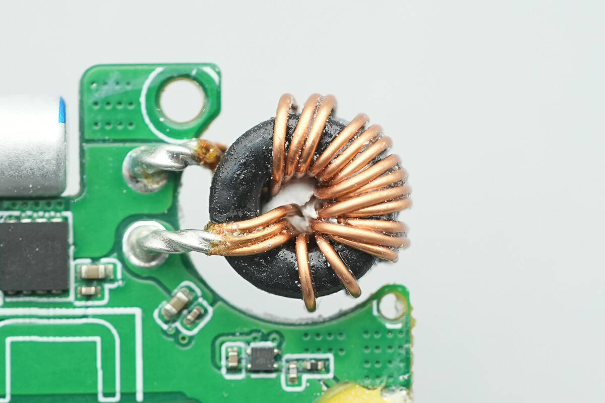
Close-up of the synchronous buck–boost toroidal inductor.
The synchronous buck–boost MOSFET is sourced from Leadteck, model LTS3818FRDY.
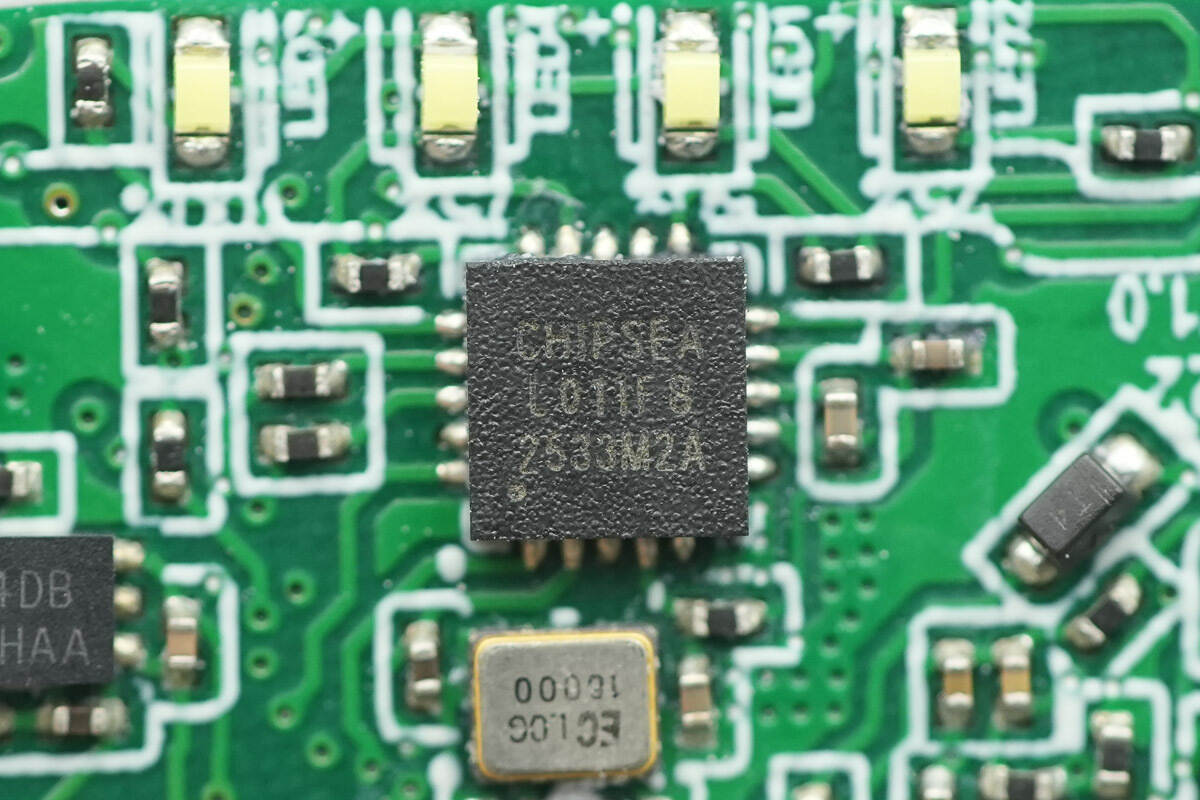
The MCU is from Chipsea, model CS32L011. It is an ultra-low-power microcontroller with a high-reliability 32-bit core, capable of operating at a maximum frequency of 24 MHz. It features 64 KB embedded Flash, 4 KB SRAM, a 12-bit 1 Msps high-precision SAR ADC, RTC, comparators, multiple UART, SPI, I²C, and PWM interfaces.
The MCU offers high integration, strong anti-interference capability, and high reliability. It operates over a temperature range of –40 °C to 85 °C and a voltage range of 2.5 V to 5.5 V. Packaged in QFN20, it provides multiple power modes to accommodate various low-power application scenarios.
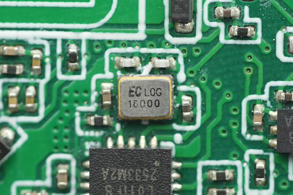
A 16MHz crystal oscillator is used to provide a stable clock reference for the CS32L011.
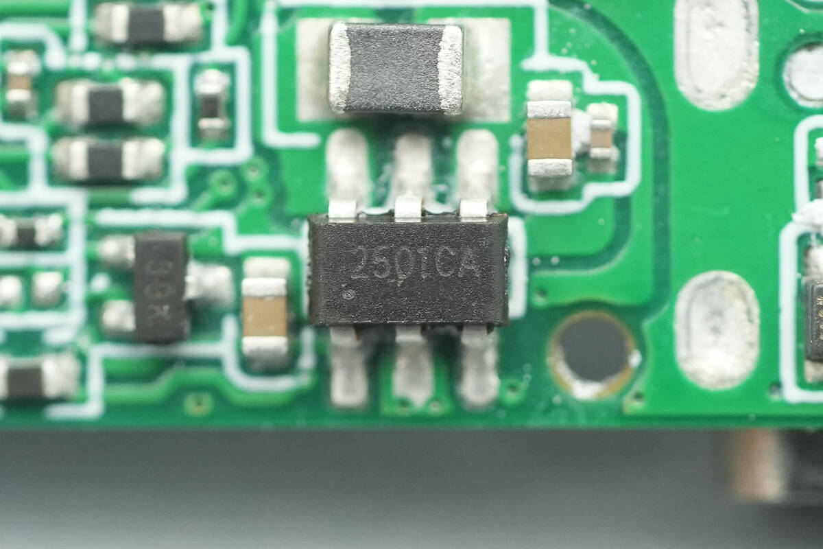
The voltage regulator chip, marked with 2501CA, is used to power the MCU.
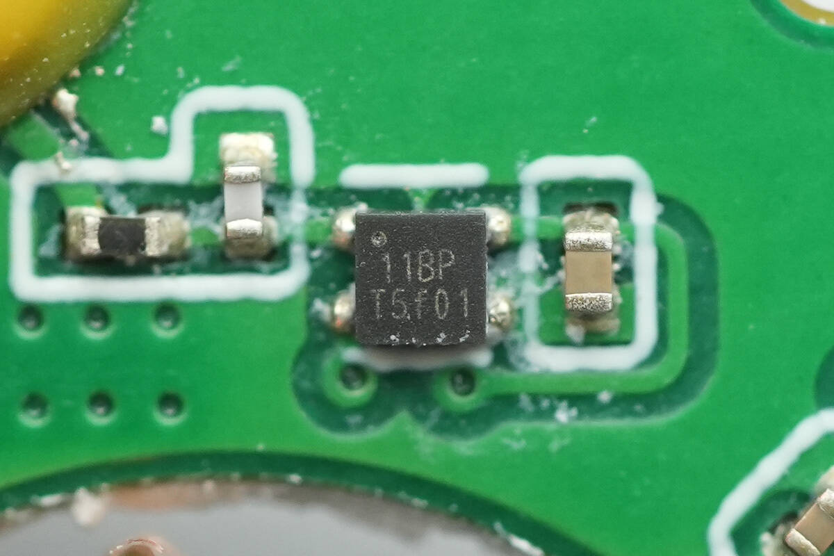
The touch detection chip uses the HYNITRON HK11BP, a low-power, single-channel capacitive touch controller, packaged in a DFN4 form factor.
The VBUS MOSFET for the USB-C interface is also from Leadteck, model LT2610FP. It is a dual NMOS with a voltage rating of 20 V and an on-resistance of 5.6 mΩ, packaged in a PDFN 3.3 × 3.3 mm 8-lead form factor.
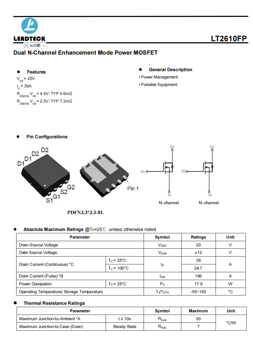
Here is the information about Leadteck LT2610FP.
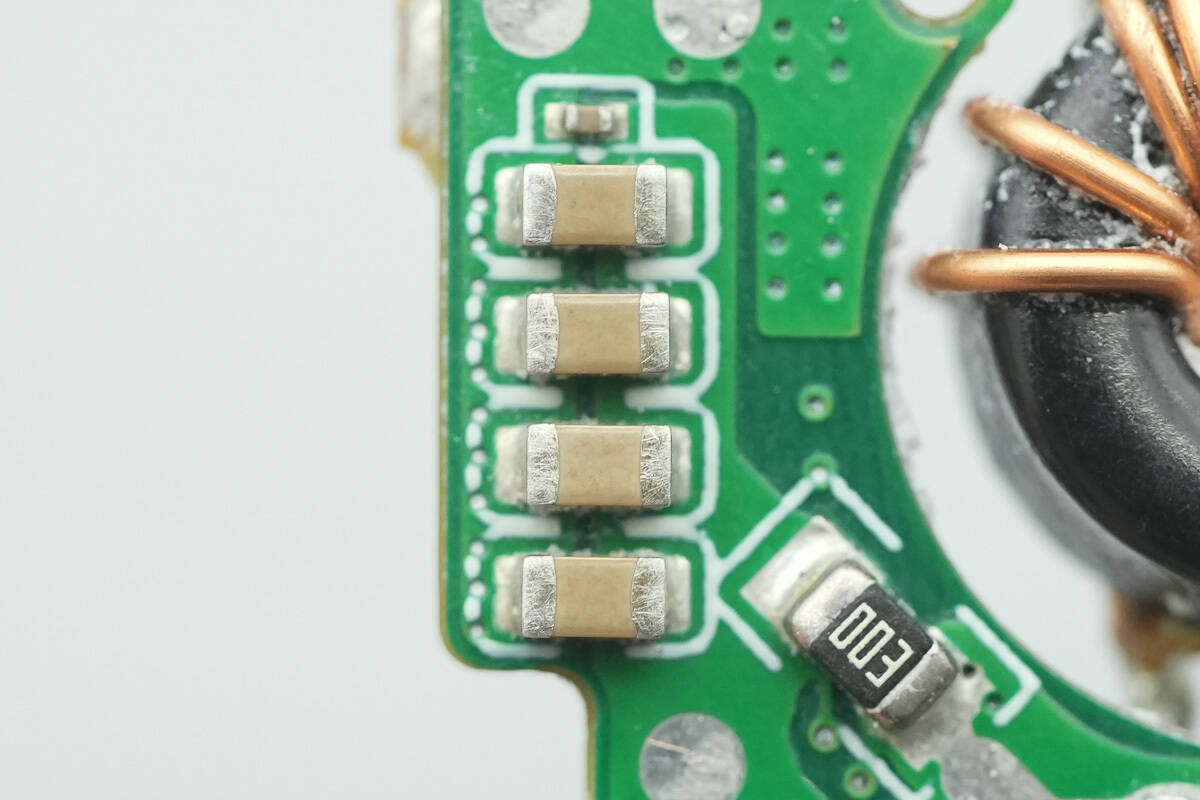
Close-up of four MLCC filter capacitors.
Close-up of five NPO resonant capacitors.
The switching MOSFET for the resonant capacitors is from Leadteck, model LTS1582FPC. It is a dual NMOS with a voltage rating of 60 V and an on-resistance of 11 mΩ, packaged in a PDFN 3.3 × 3.3 mm 8-lead form factor.
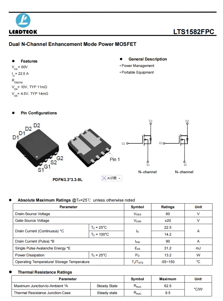
Here is the information about Leadteck LTS1582FPC.
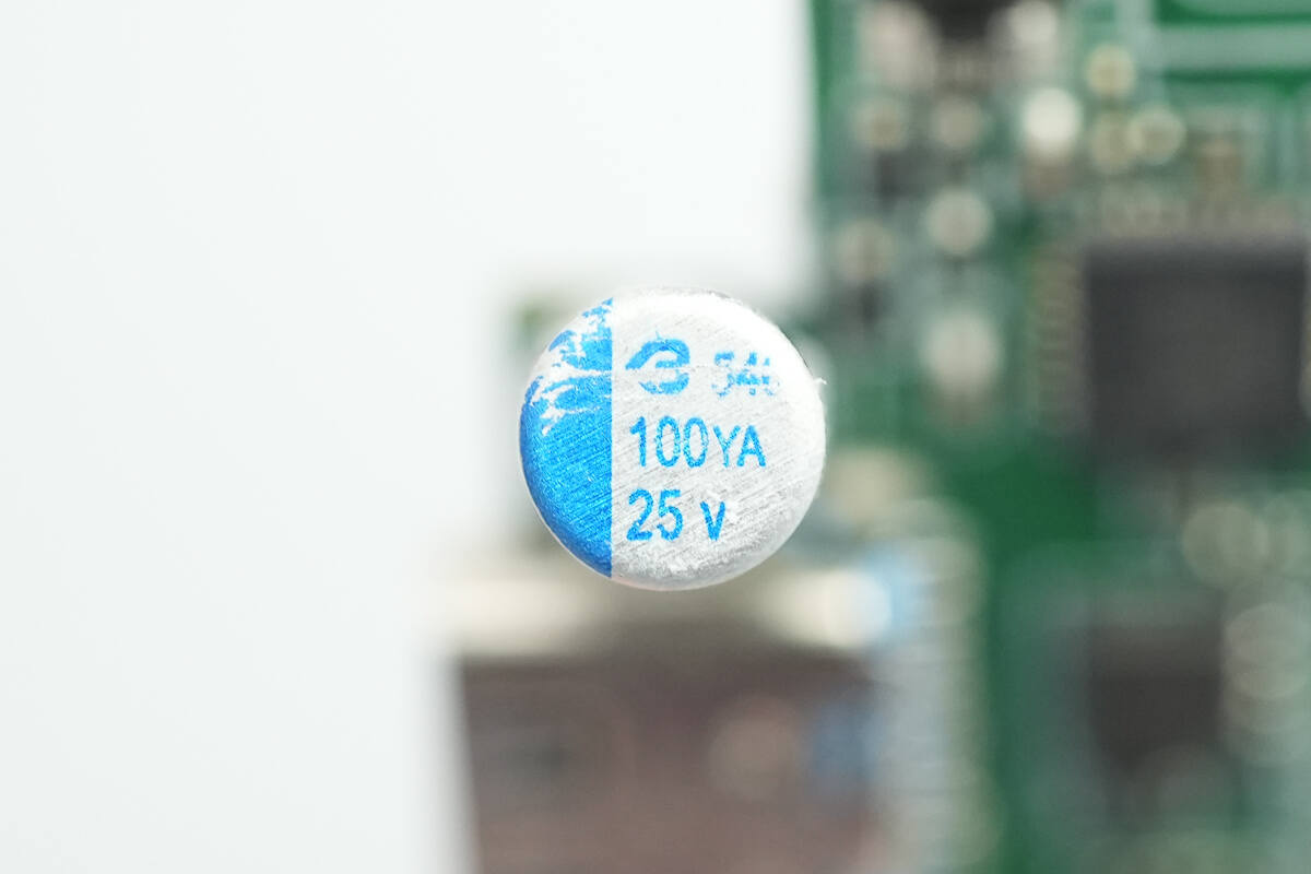
The solid capacitor is from BERYL, with a rating of 100 μF, 25 V.
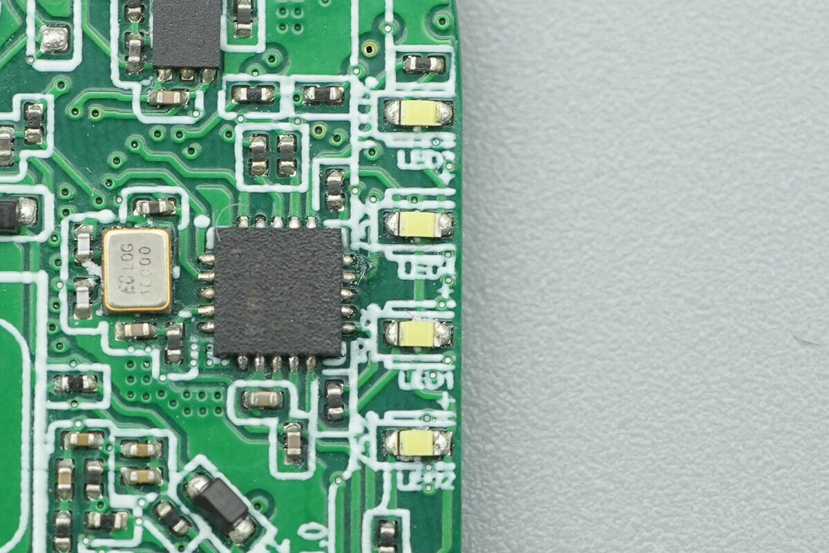
Close-up of four side-by-side LED light beads.
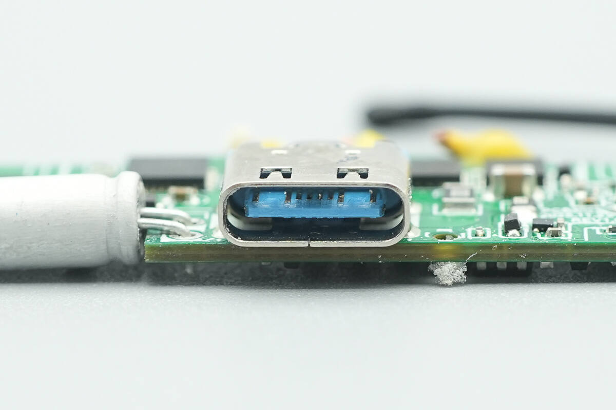
Close-up of the USB-C socket.
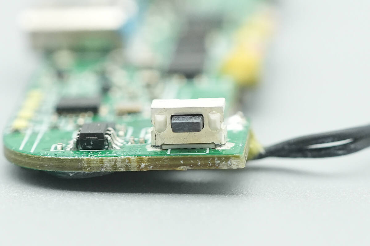
Close-up of the power button.
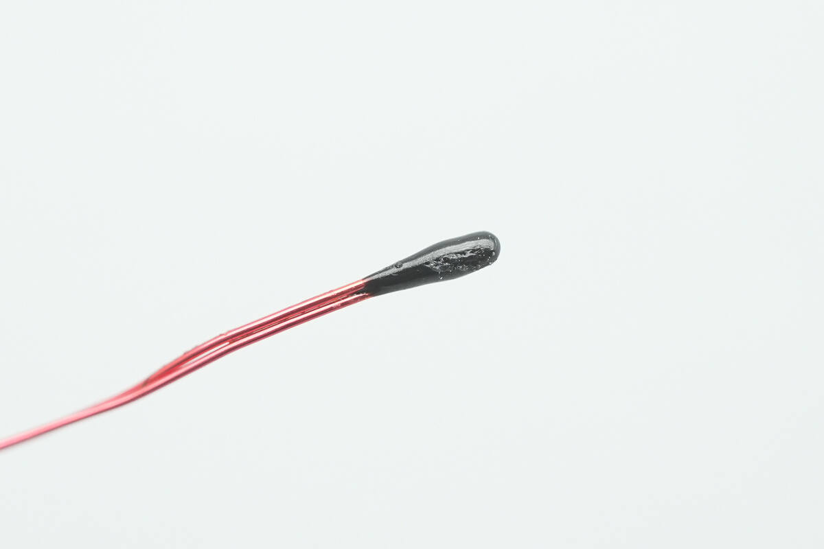
Close-up of the NTC thermistor.

Well, those are all components of the Anker Nano 5000mAh Magnetic Power Bank.
Summary of ChargerLAB
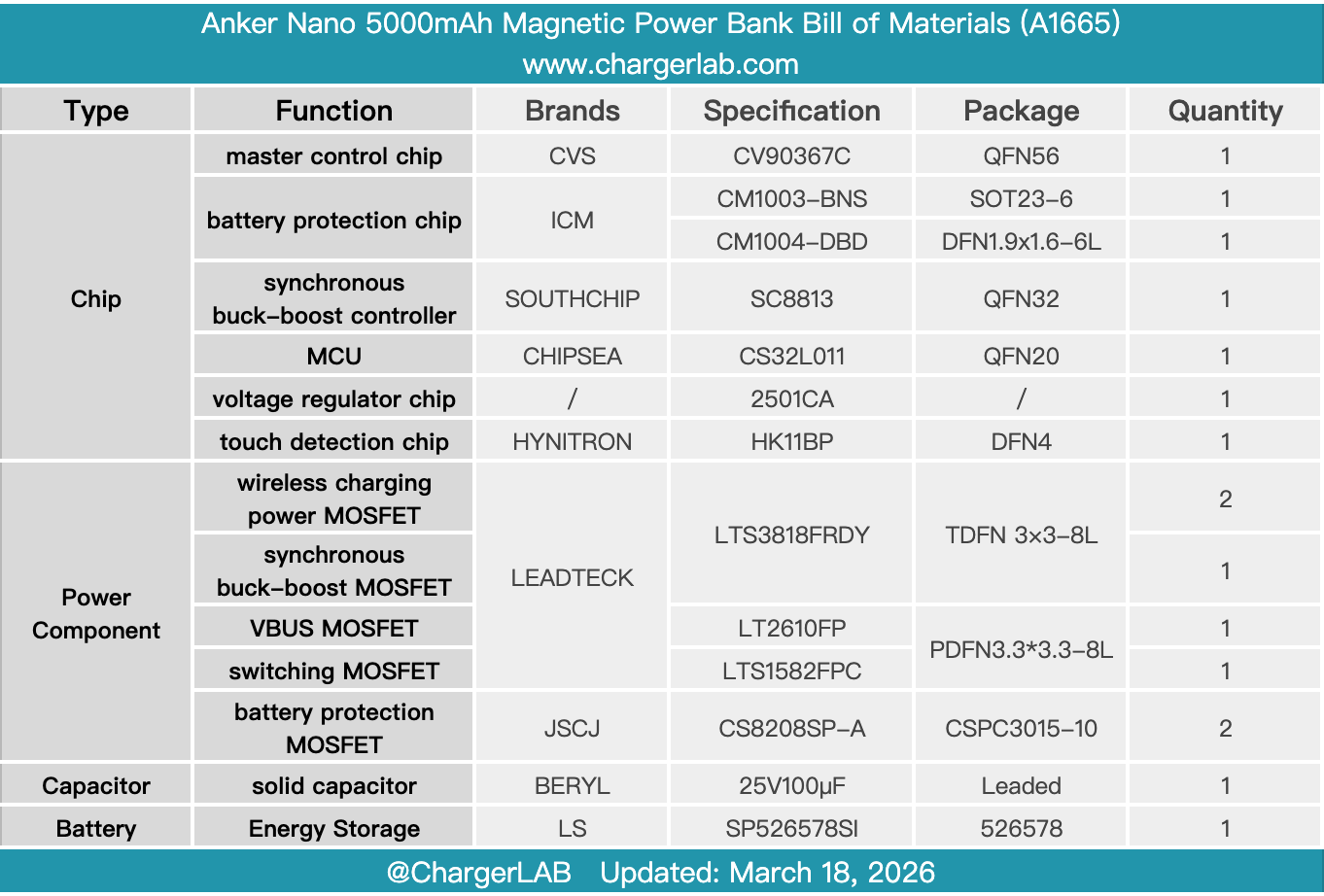
Here is the component list of the Anker Nano 5000mAh Magnetic Power Bank for your convenience.
The power bank is about 8.7 mm thick, featuring a metal mid-frame and dual-sided skin-friendly material for a comfortable grip. It houses a 5000 mAh battery and supports 20W wired input/output as well as 7.5W wireless output.
After taking it apart, we found that it uses the CVS CV90367C highly integrated wireless charging SoC. This chip integrates wireless charging control, communication decoding, Q-factor detection, FOD (foreign object detection), pre-driving, and other functions, and is compatible with multiple wireless charging standards including 5 W BPP, Apple MagSafe 7.5 W, and 15 W EPP.
The battery protection circuit uses a dual-protection IC scheme with the iCM CM1003-BNS and CM1004-DBD, paired with JSCJ CS8208SP-A battery protection MOSFETs to form a complete protection solution. Wired charging and discharging management is handled by the SouthChip SC8813, while other components such as the Chipsea CS32L011 MCU and HYNITRON HK11BP touch detection chip participate in overall system control.
The battery pack consists of a single LS 5000 mAh pouch cell. The corresponding motherboard area is covered with insulating and heat-resistant materials, and the board surface is overlaid with thermal conductive material. The top of the enclosure includes a large graphene heat spreader, and NTC thermistors are installed at both the battery and wireless charging coil locations for temperature monitoring. The build quality is solid, with well-thought-out protective design.
Related Articles:
1. Teardown of HuntKey 45W GaN Charger (HKC04520023-0J2)
2. Teardown of HONOR 120W GaN Charger (HN-200600C02)
3. Teardown of Great Wall 800W Platinum SiC Server Power Supply (GW-CRPS800N2)