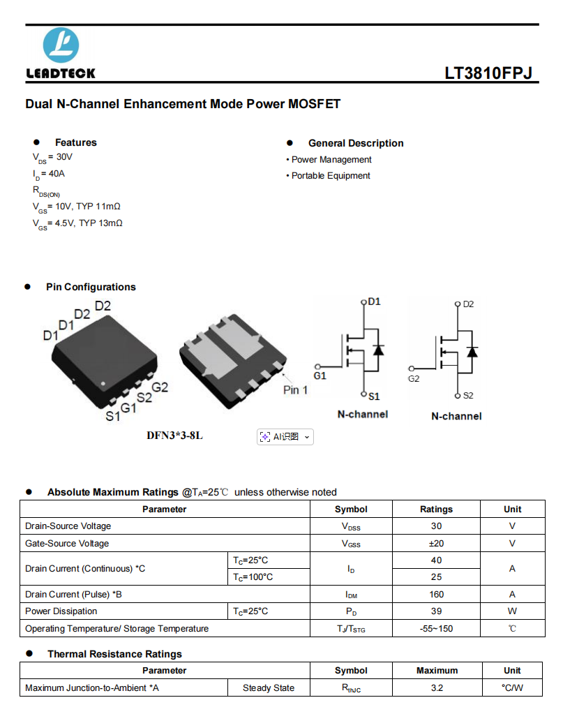
Introduction
We are disassembling Anker's latest magnetic wireless power bank, which features an upgraded S.2 flame-retardant design and UL2056 Level 2 safety protection. It houses two ATL cells sourced from the same manufacturer as Apple, each with a capacity of 5,000mAh, connected in series for a total capacity of 10,000mAh. The power bank supports fully transparent data tracking via a web interface, allowing users to monitor battery health, temperature, cycle count, voltage, current, and other detailed information in real time, making it a distinctive product among current similar devices.
It is equipped with a USB-C port, supporting 27W wired charging and 7.5W wireless charging, and features a digital display that shows remaining battery life and charging time. The device also includes a foldable stand. Next, we will take a closer look at the design of this product.
Product Appearance
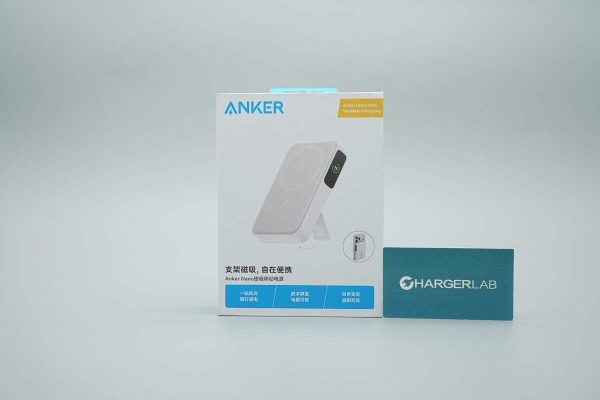
The front of the packaging features the Anker logo, a product rendering, the product name, and selling points.
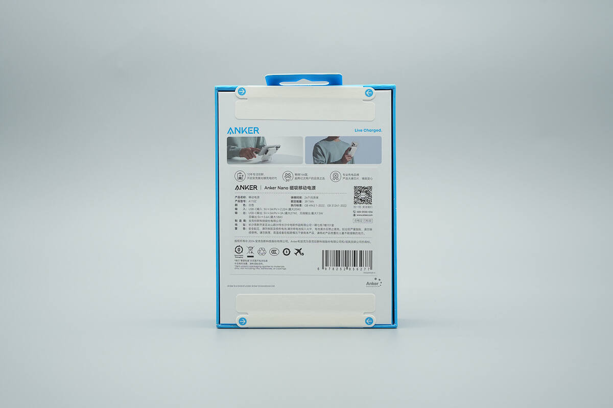
The back of the packaging displays the key features, specifications, manufacturer information, safety notices, and production date.
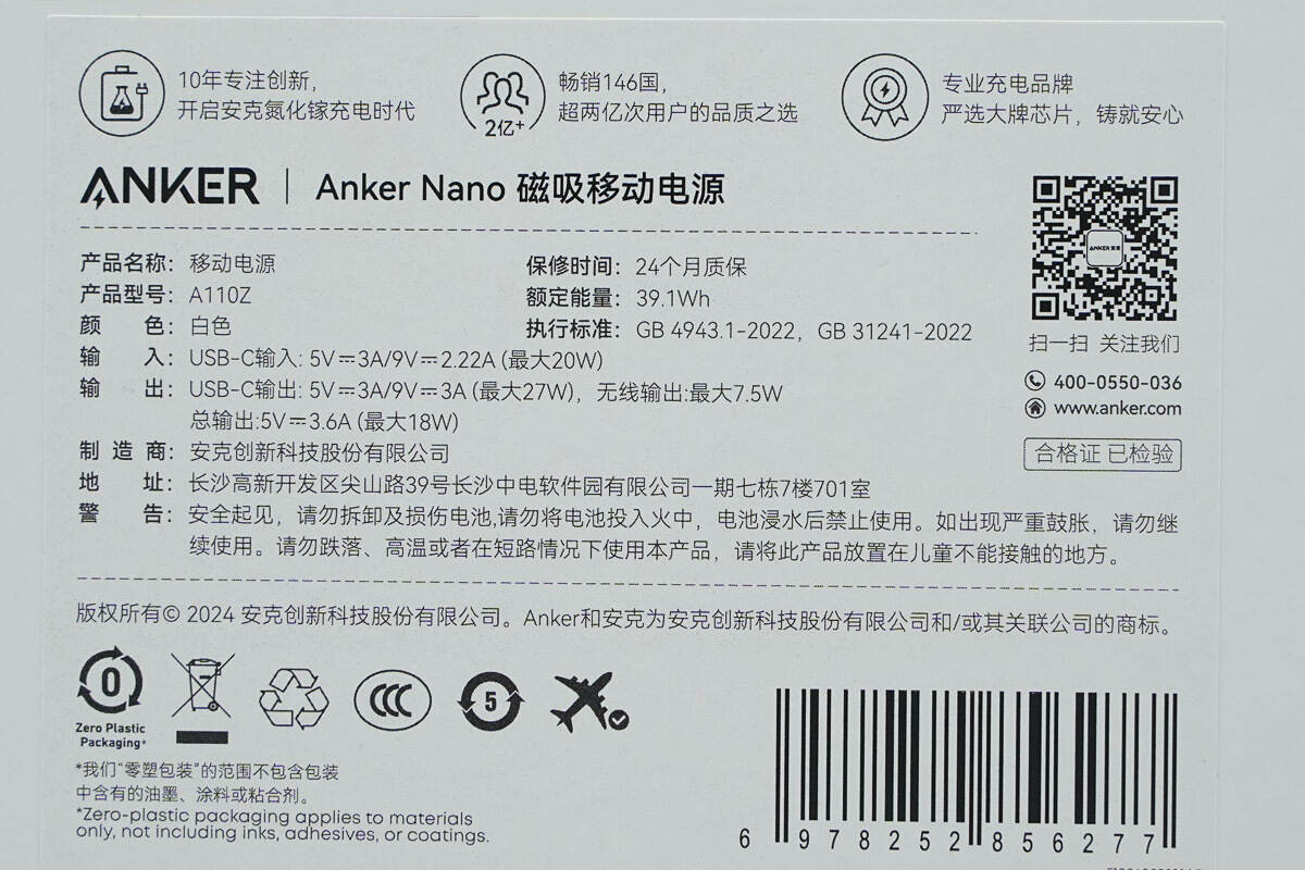
Model: A110Z
Color: White
Warranty: 24-month warranty
Rated Energy: 39.1Wh
Standards: GB 4943.1-2022, GB 31241-2022
Manufacturer: Anker Innovations Technology Co., Ltd.
Input: USB-C Input: 5V⎓3A / 9V⎓2.22A (max 20W)
Output: USB-C Output: 5V⎓3A / 9V⎓3A (max 27W)
Wireless Output: Up to 7.5W
Total Output: 5V⎓3.6A (max 18W)
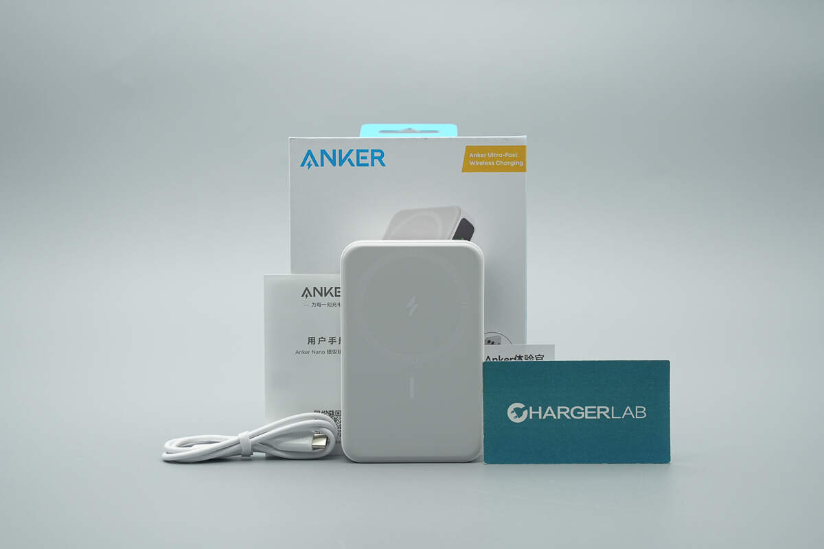
The package includes the power bank, a dual USB-C cable, and a user manual.
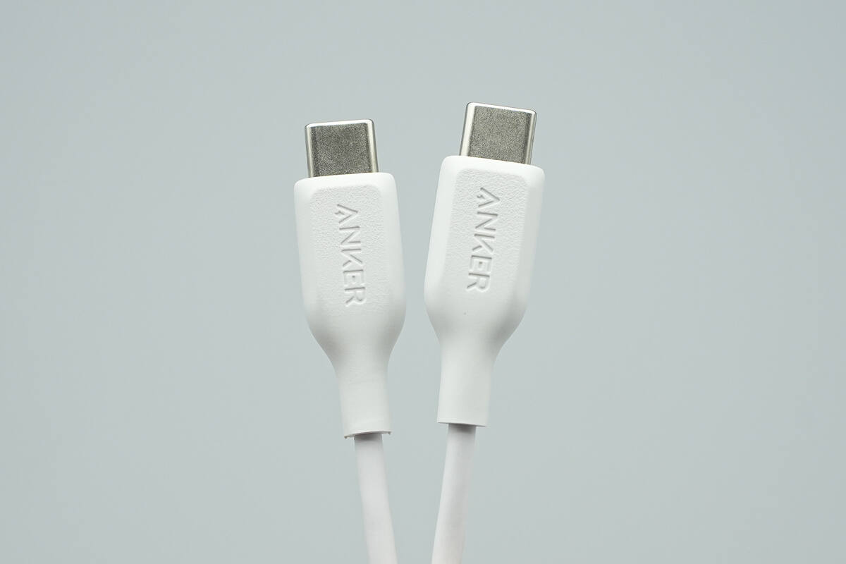
The dual USB-C cable features an integrated molded coating with an extended strain relief at the connector end, and is marked with the ANKER logo.
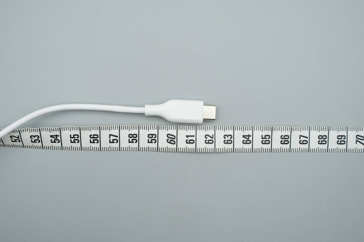
The length is about 62 cm (24.41 inches).
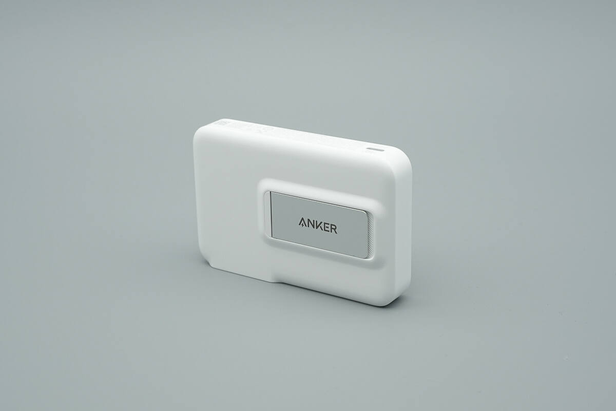
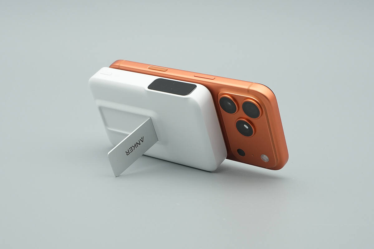
The body of the device is primarily white, with smoothly rounded edges and corners. In the center of the back, there is a recessed stand, which is marked with the ANKER logo.
Anker has reportedly upgraded the materials used for the casing, enabling the product to meet the S.2 needle-flame test certification and flame-retardant requirements, further enhancing its safety.
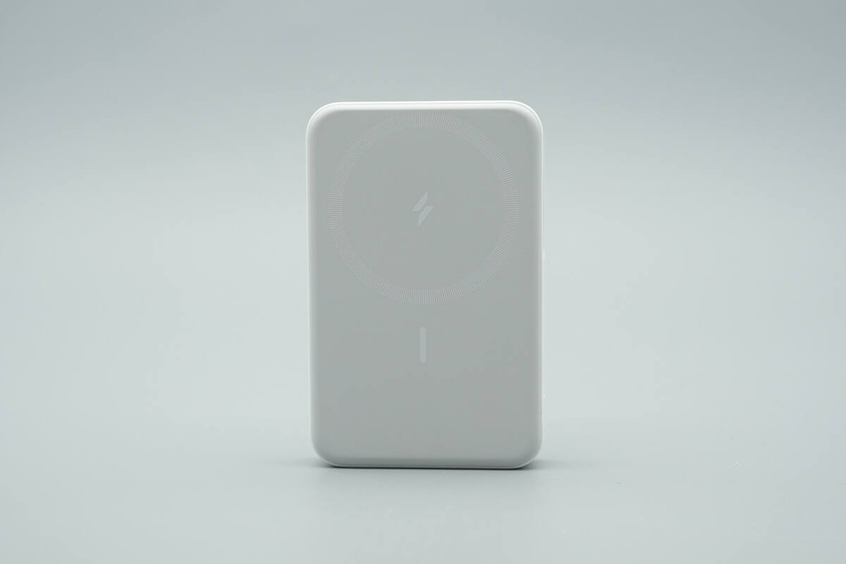
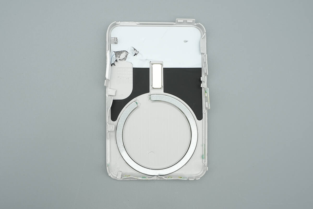
The magnetic charging panel features a circular wireless charging area at its center.
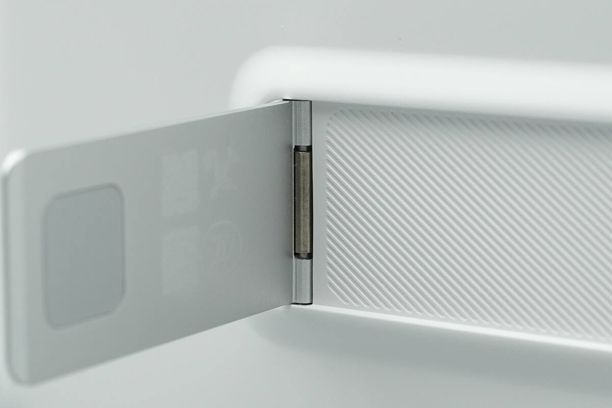
When the stand is unfolded, a large internal area with a diagonal pattern design becomes visible.
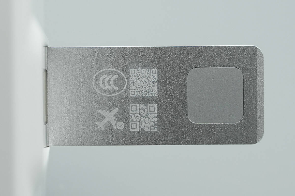
The inner side of the stand is marked with certification labels and other information, while the square magnet on the right is used to secure the stand.
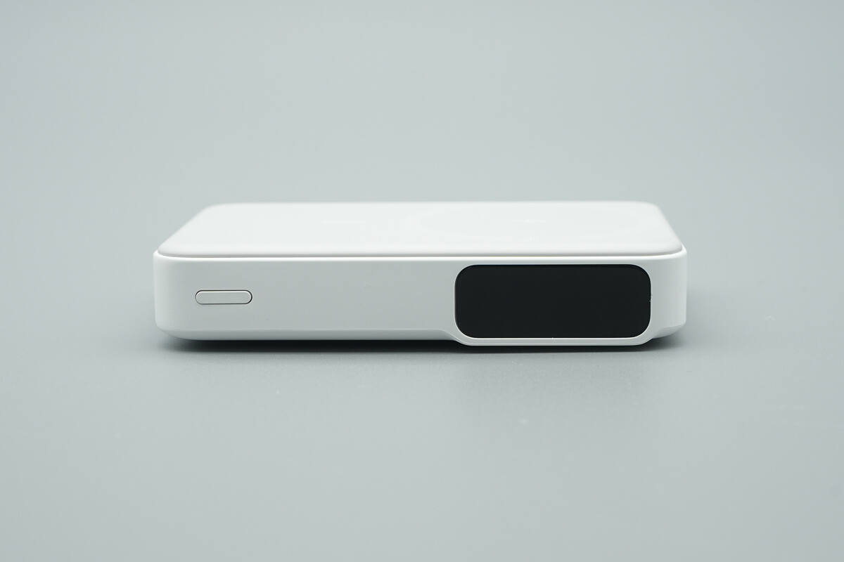
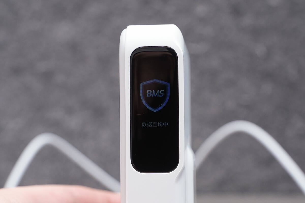
This side features the power button and a digital display screen.
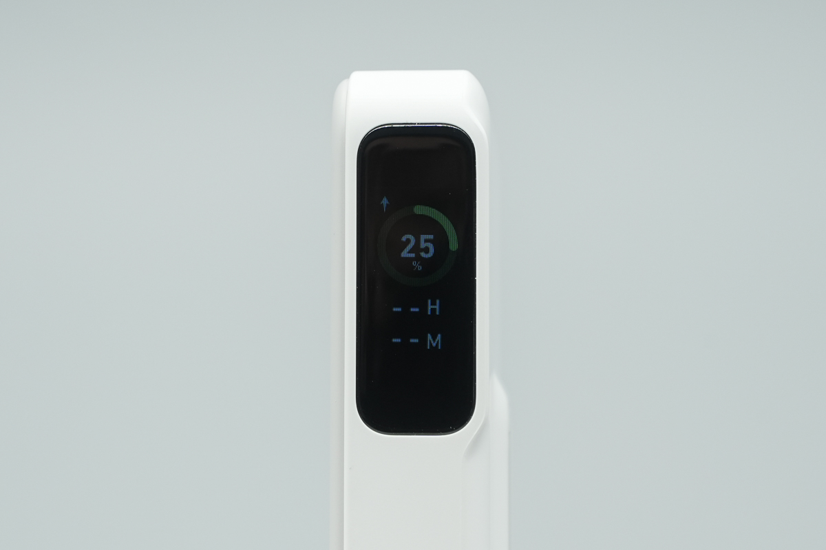
The screen displays the remaining battery level and the estimated charging time.
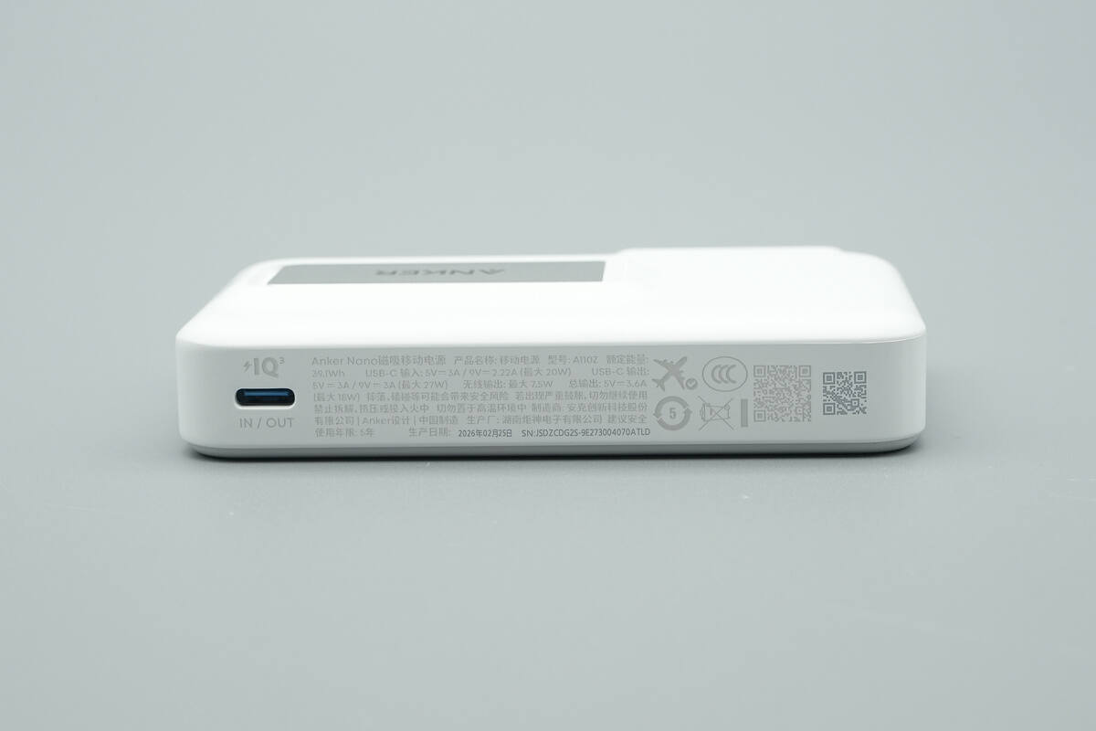
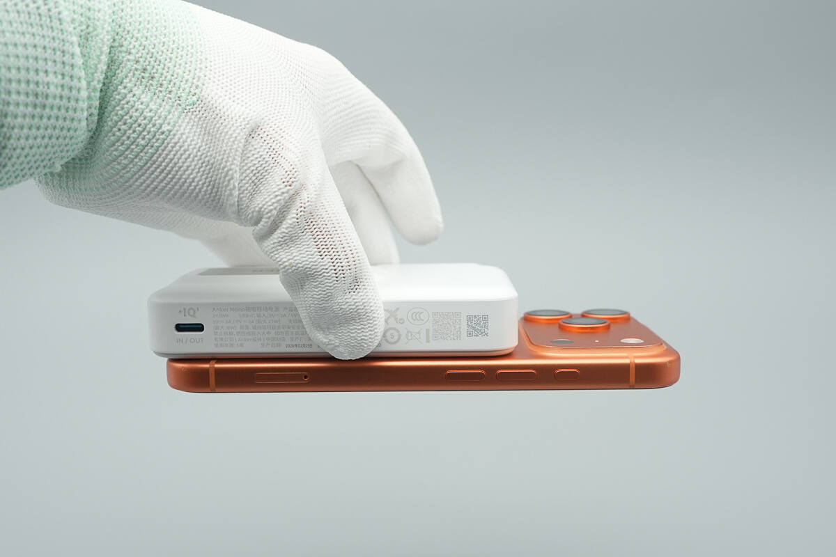
This side features a USB-C port that supports both input and output, with the specifications printed nearby.
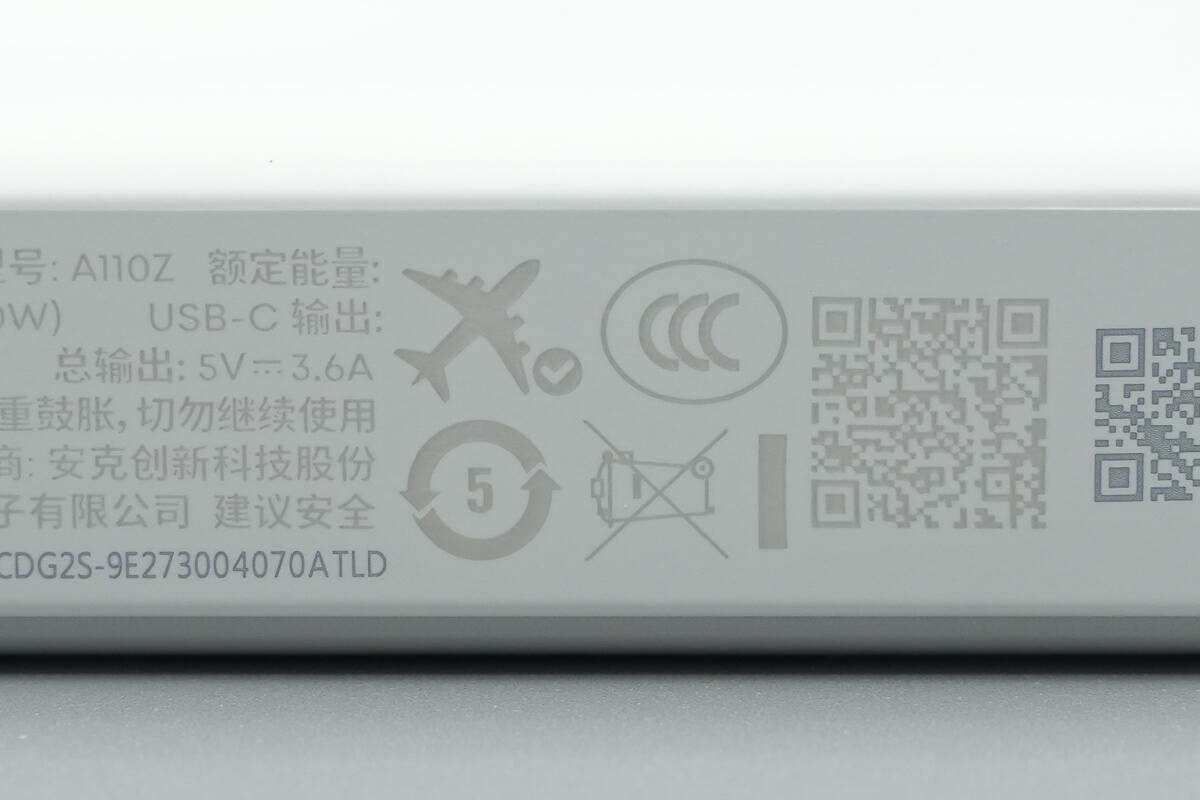
The product has passed CCC certification.
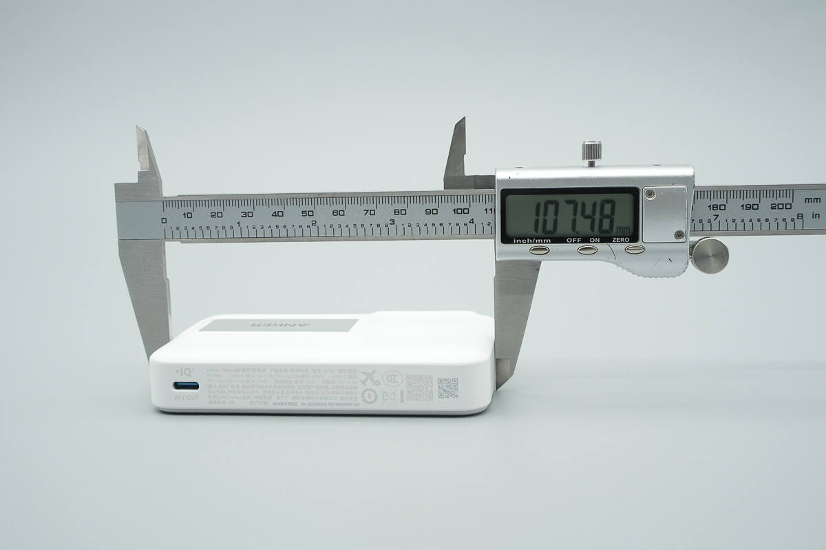
The length of the power bank is about 107.48 mm (4.23 inches).
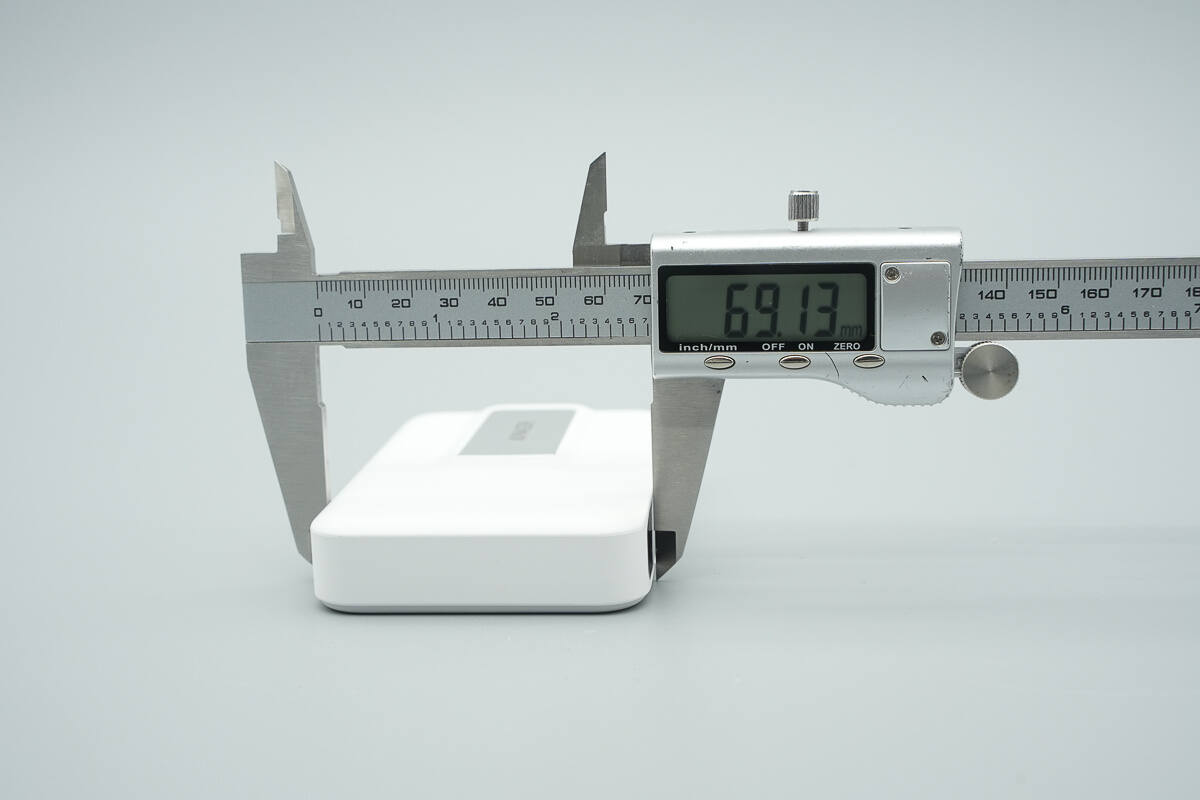
The width is about 69.13 mm (2.72 inches).
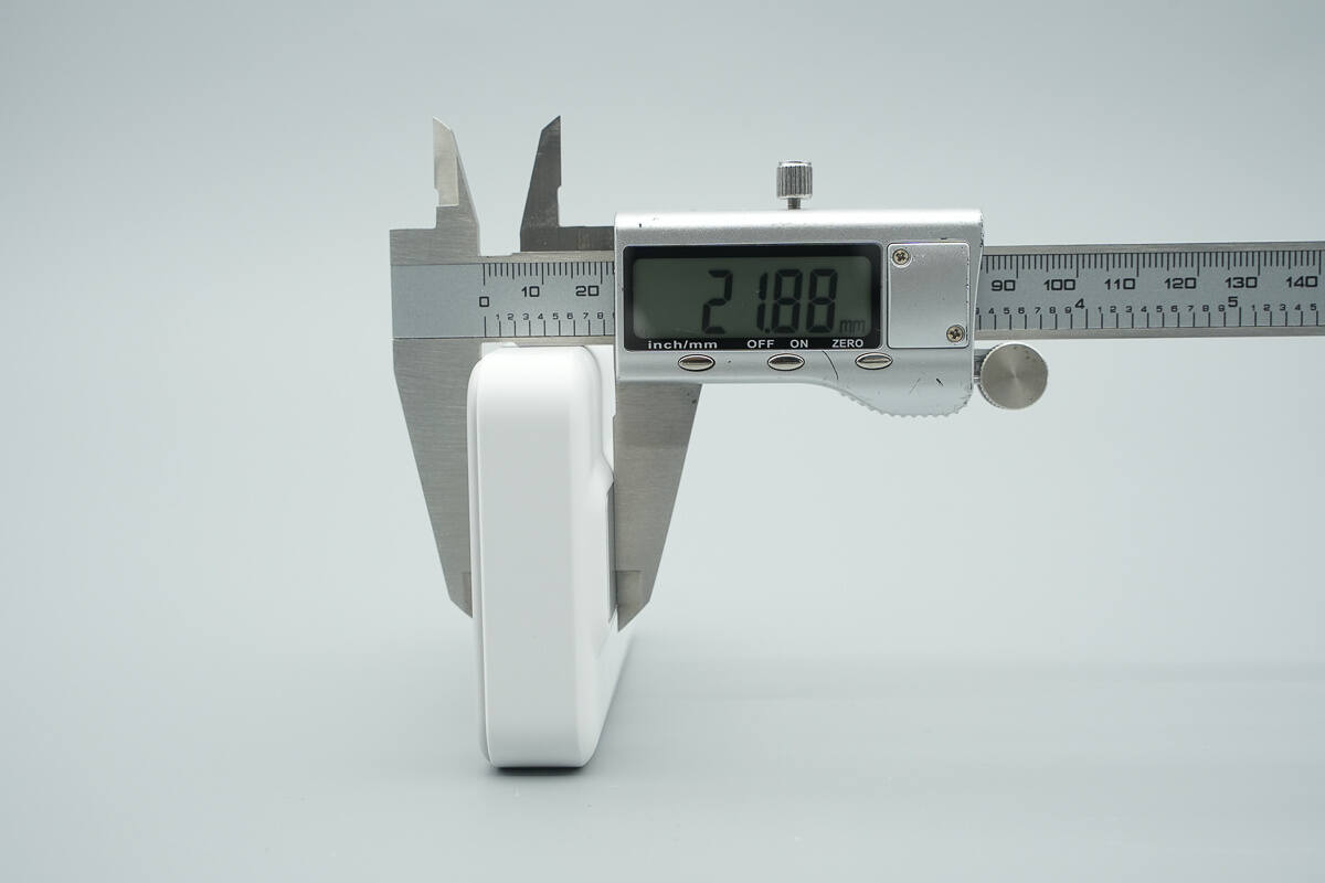
The thickness is about 21.88 mm (0.86 inches).
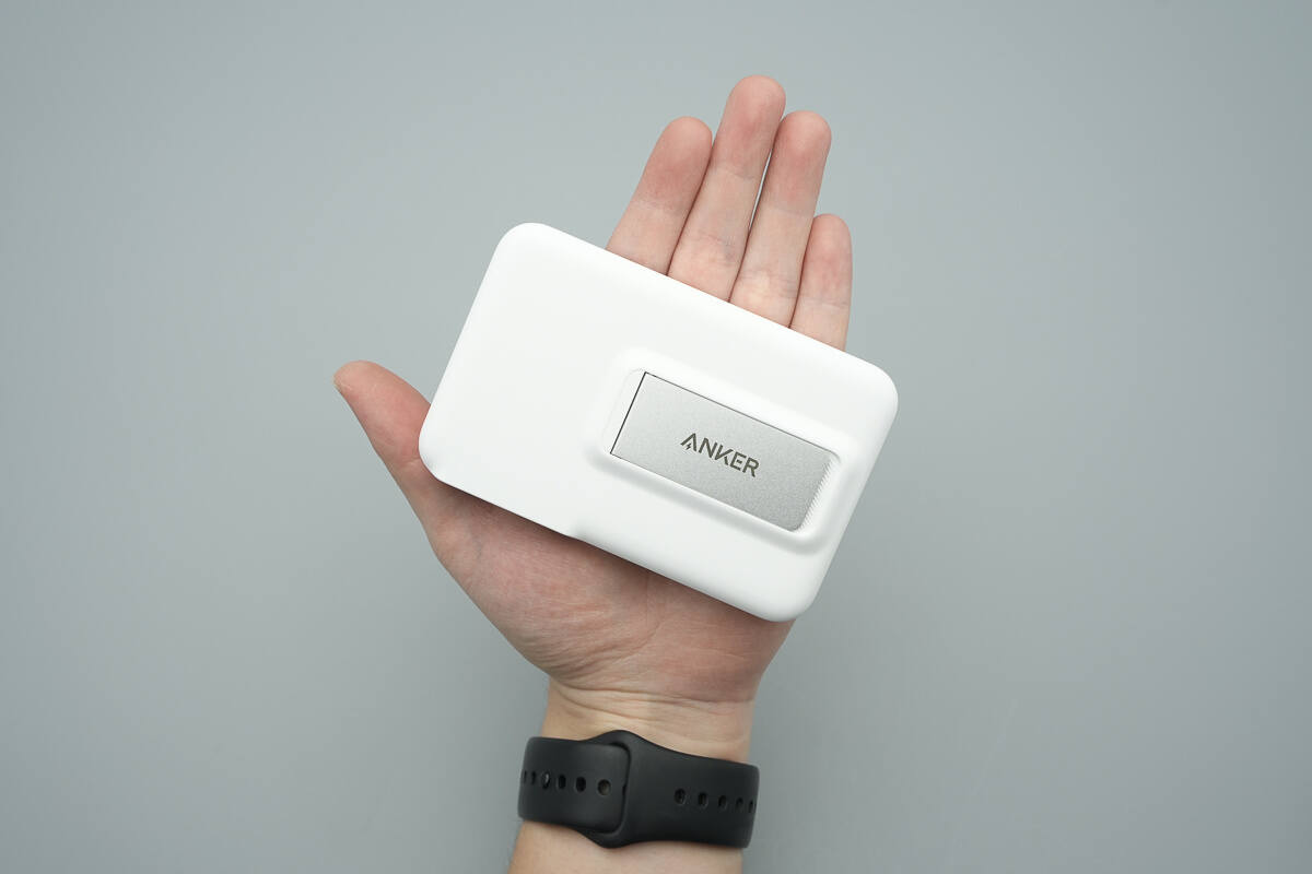
That's how big it is in the hand.
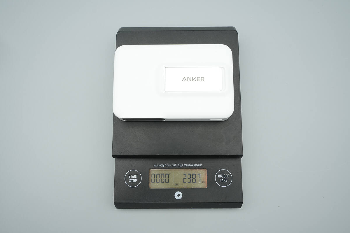
The weight is about 238.7 g (8.42 oz).
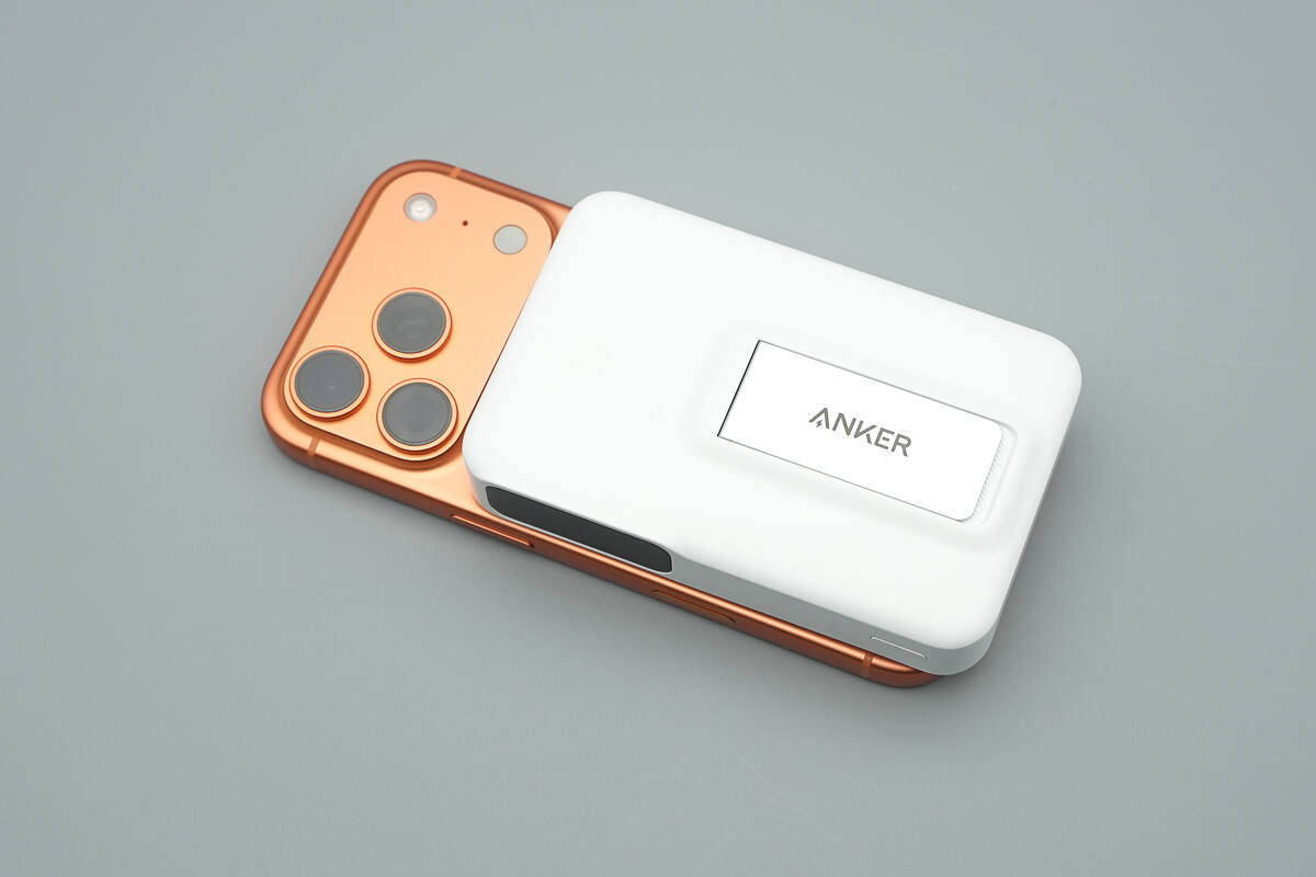
When wirelessly charging an iPhone 17 Pro Max, it does not obstruct the phone’s camera module.
Even when the phone is inverted, it will not fall off.
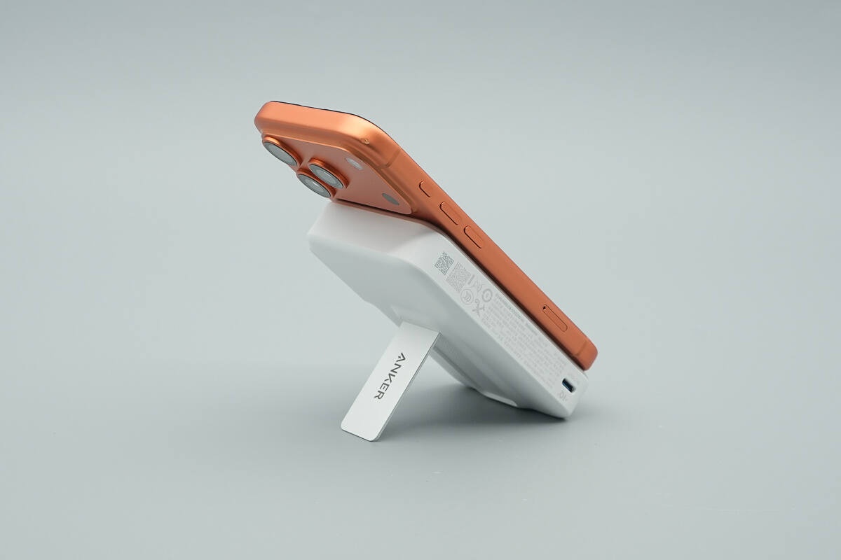
Convenient to use while charging when the stand is unfolded
It can also be used horizontally.
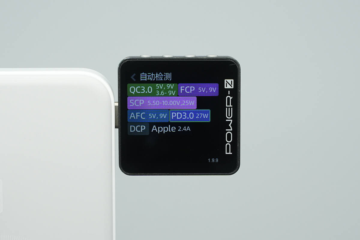
ChargerLAB POWER-Z KM003C shows that the USB-C port supports QC3.0, SCP, FCP, AFC, PD3.0, DCP, and Apple 2.4A charging protocols.
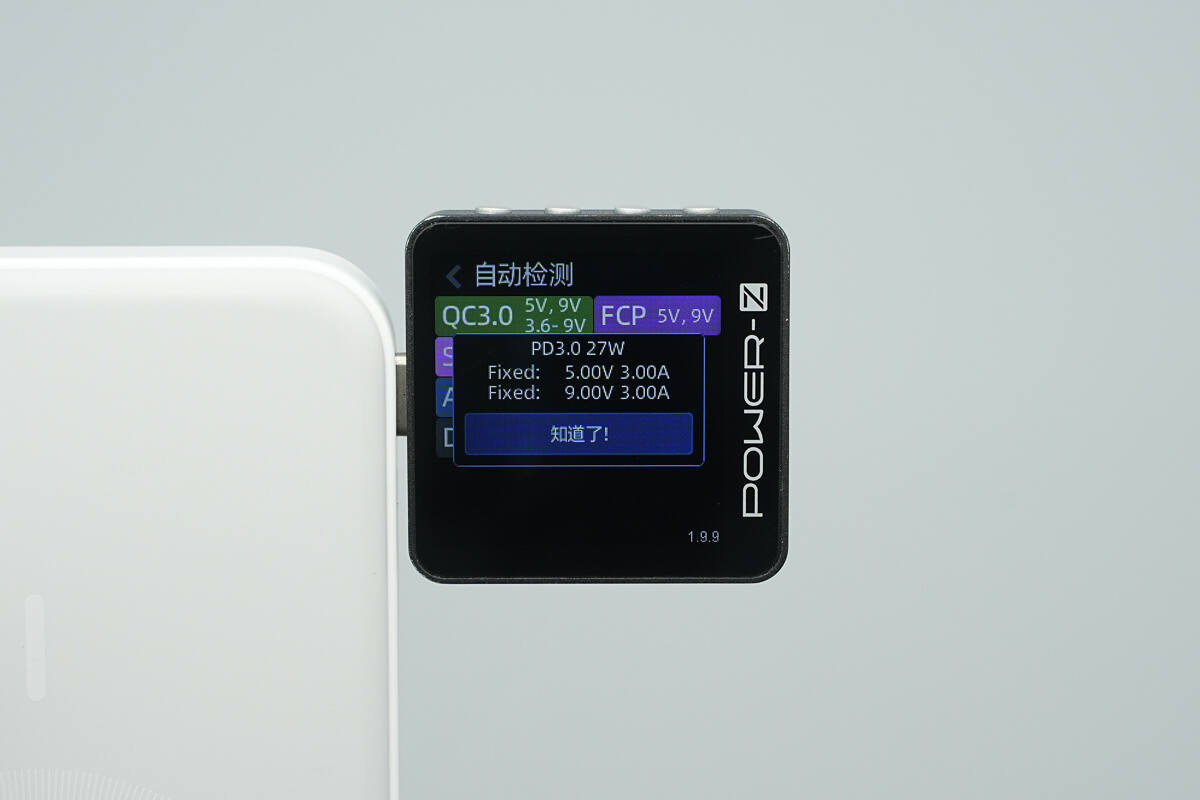
And it has two fixed PDOs of 5V3A and 9V3A.
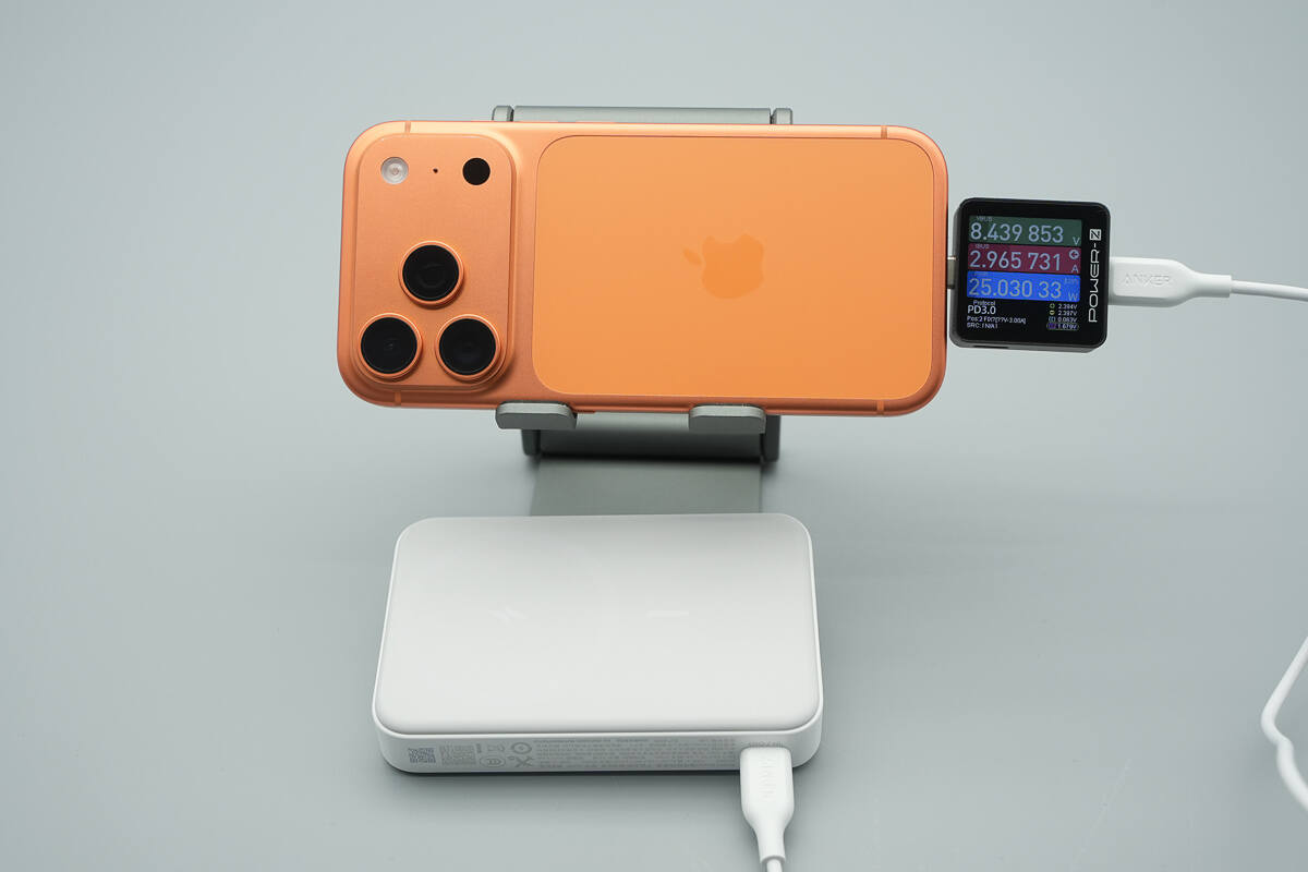
When charging the iPhone 17 Pro Max via USB-C, the power output is 25.03 W.
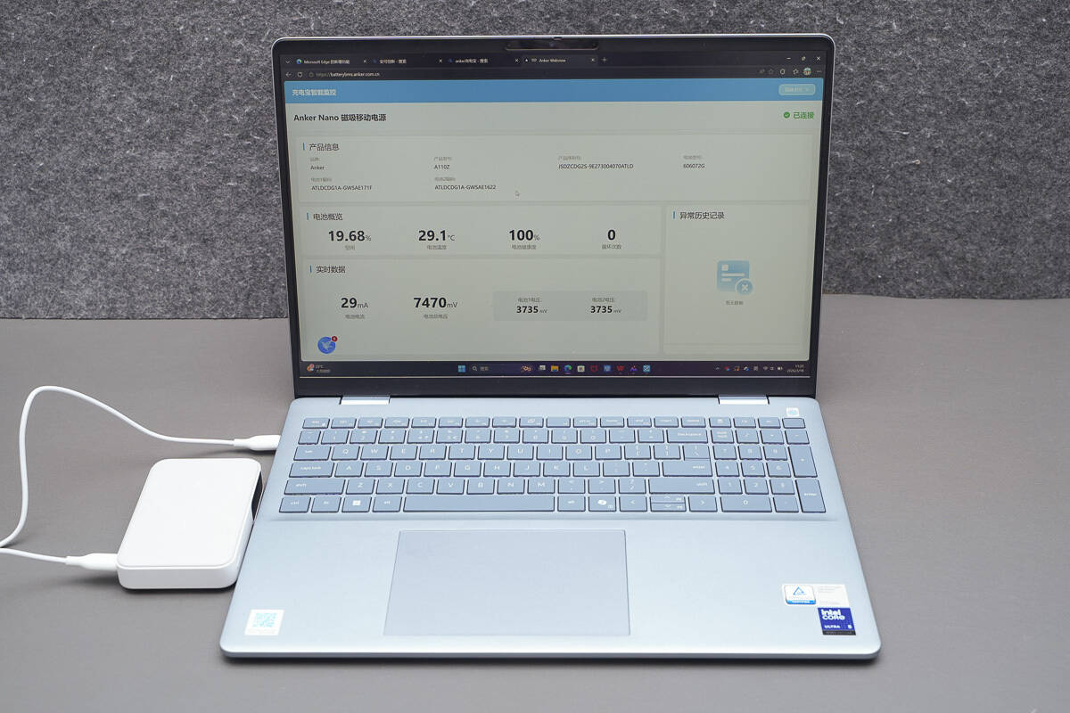
It supports full transparent data tracking. By connecting the power bank to a computer with a data cable, you can access the smart monitoring website to view the power bank’s current operating status and battery data in real time.
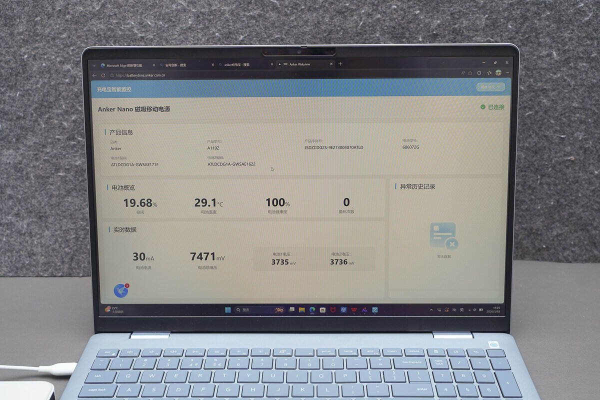
On the monitoring page, you can view detailed information such as the product model, serial number, battery model, battery code, as well as battery level, temperature, health status, cycle count, battery current, total voltage, and individual cell voltages.
At the same time, the power bank’s digital display will also show the current status information.
Teardown
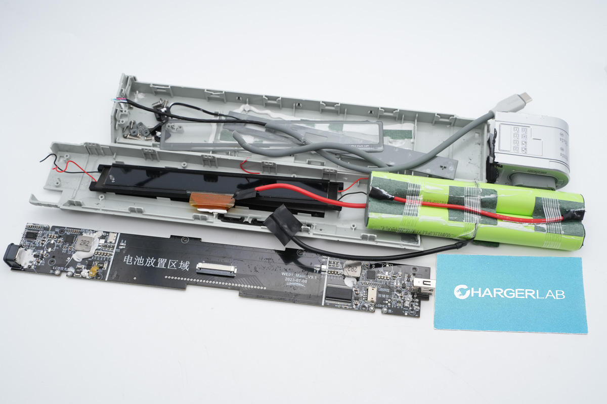
Next, let's take it apart to see its internal components and structure.
Open the casing along the seams and secure it with the clips.
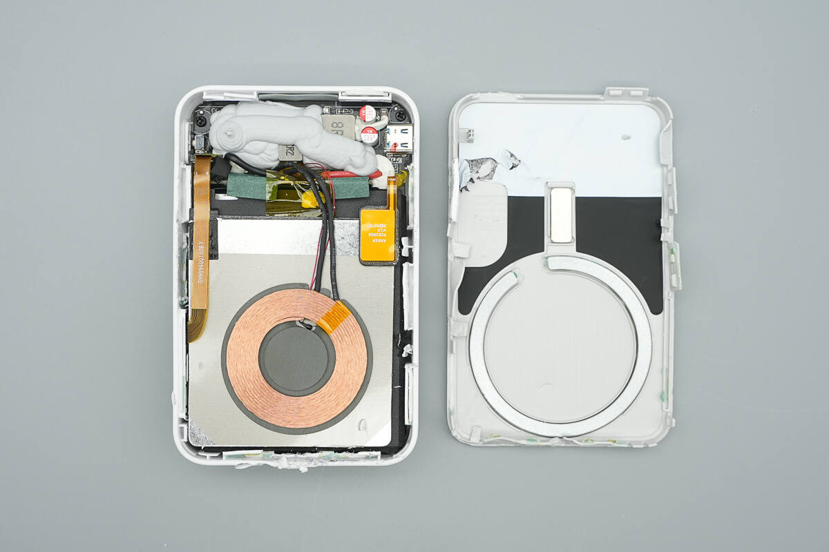
The inside of the casing has a circular magnet and a vertical positioning magnet.
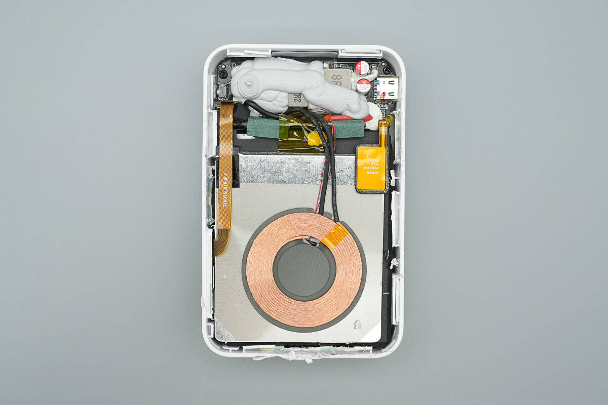
The top inside the casing houses the PCBA module, covered with gray thermal adhesive. Below it are the battery and the wireless charging module.
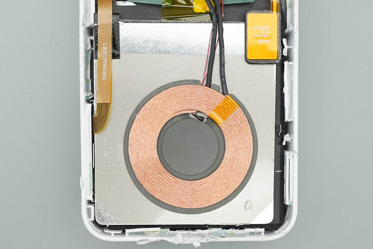
The charging coil’s wires are connected to the PCBA, and a metal plate separates the coil from the battery cells.
The PCB is secured with two screws.
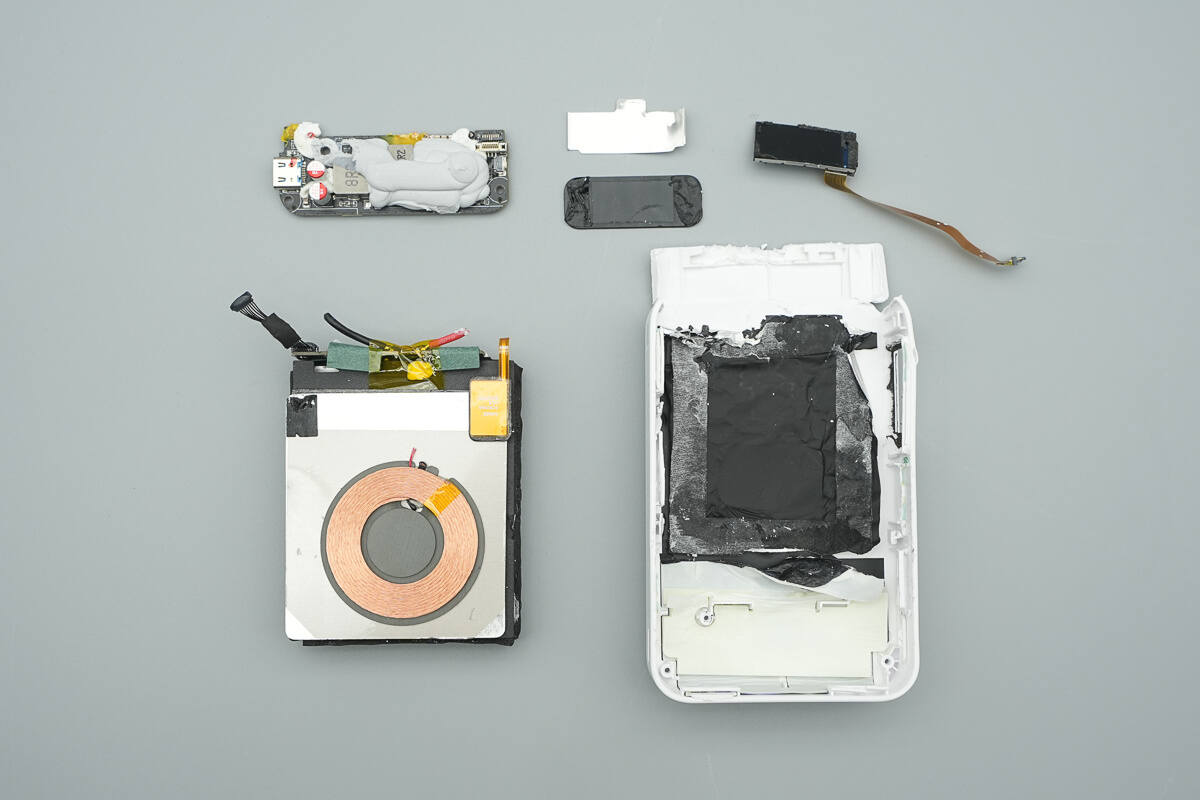
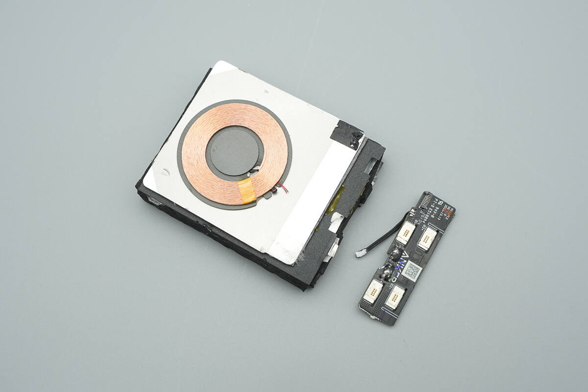
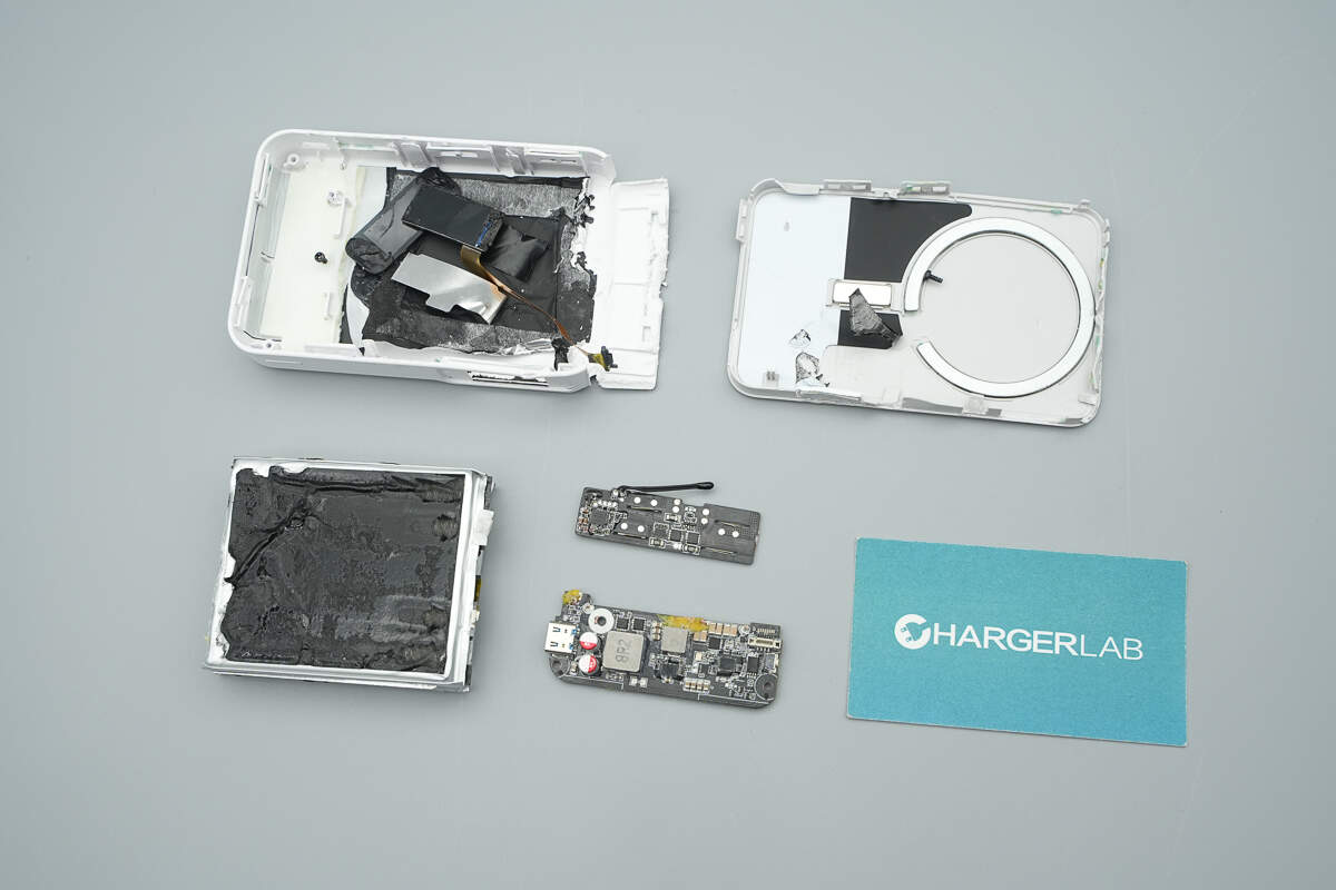
Separate the PCB, digital display module, and battery wireless charging module.
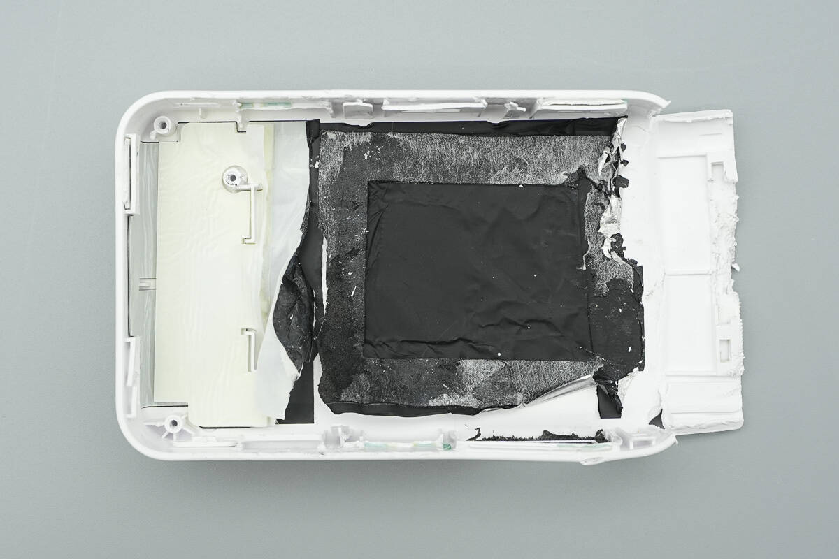
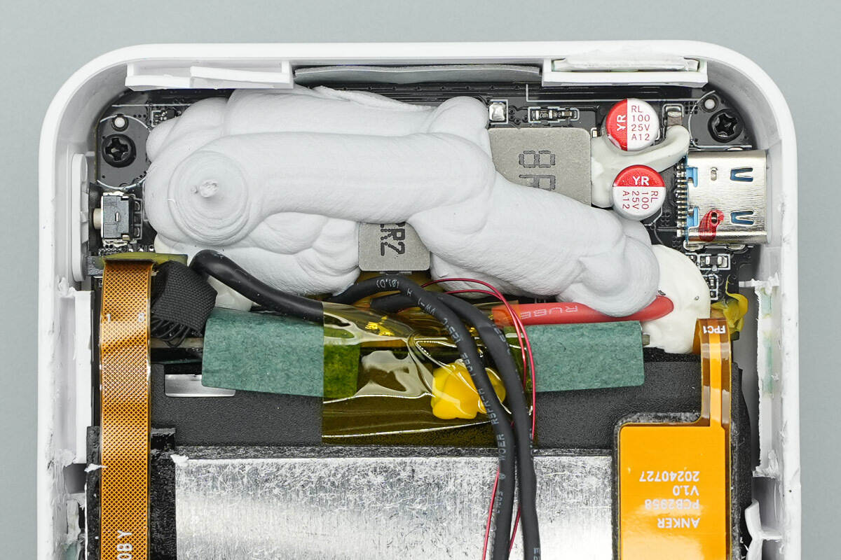
The bottom casing has black foam in the battery area and a white plastic sheet in the PCB area.
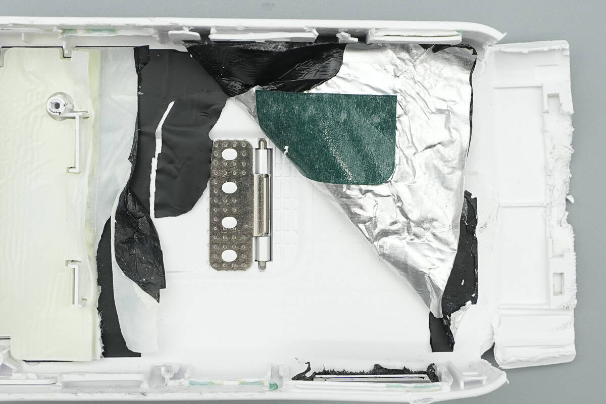
The hinge of the stand is insulated with kraft paper.
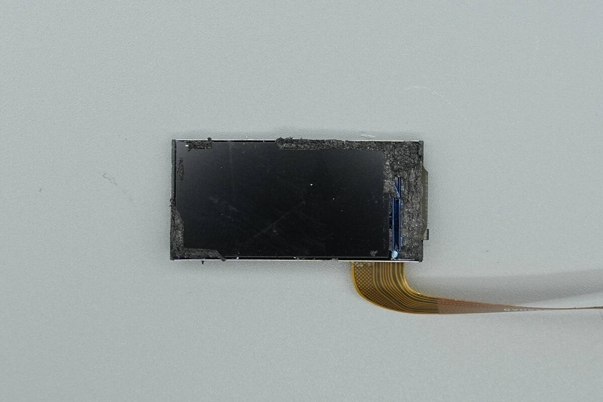
The display is connected to the PCB via flexible wires.
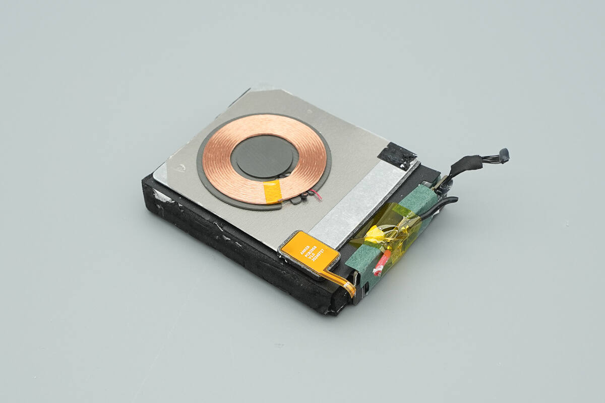
The battery and wireless charging module are covered with a metal plate.
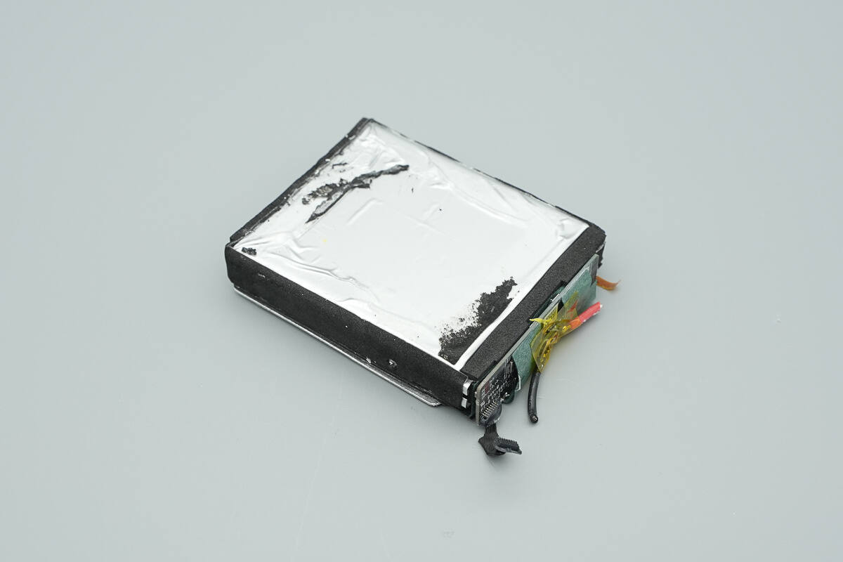
Black foam surrounds the edges of the battery cells.
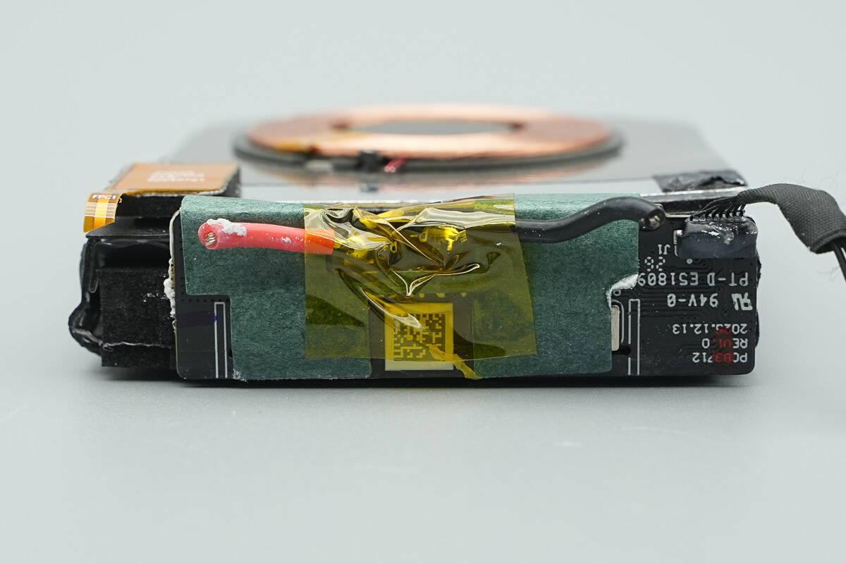
The battery protection PCB is mounted on the battery cell module, with kraft paper insulating the solder joints and secured with high-temperature tape.
Separate the battery protection PCB from the battery cell module.
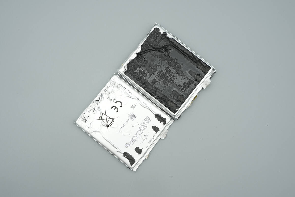
The battery module consists of two soft-pack cells connected in series, with both cells having identical specifications.
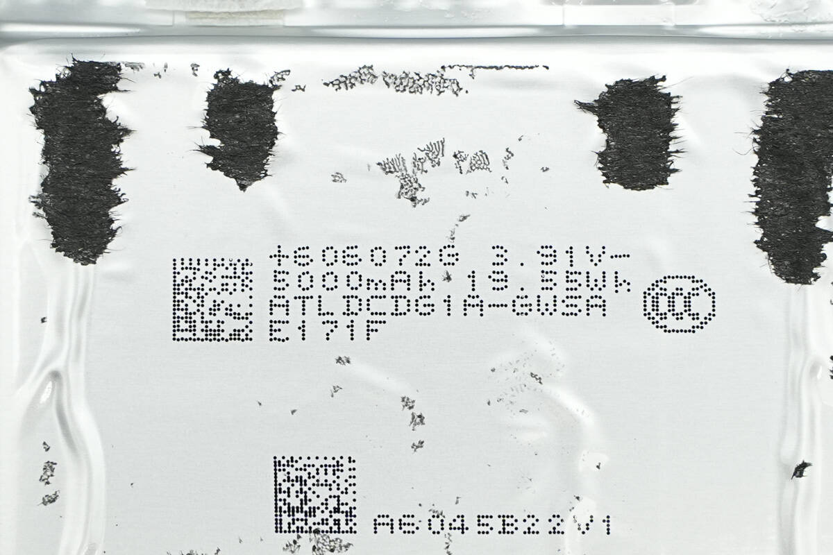
The cells are sourced from ATL, model 606072G, with a rated capacity of 5000 mAh and rated energy of 19.55 Wh. The nominal voltage is 3.91 V, and they are CCC certified.
According to official information, these cells have passed five rigorous safety tests—nail penetration, compression, thermal chamber, overcharge, and lithium plating—providing an enhanced safety experience with every charge.
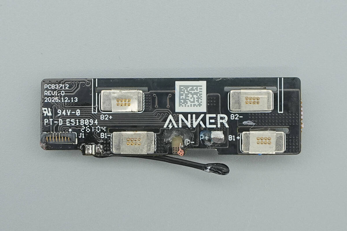
The front side of the battery protection PCB features multiple spring contacts for connecting to the battery cells.
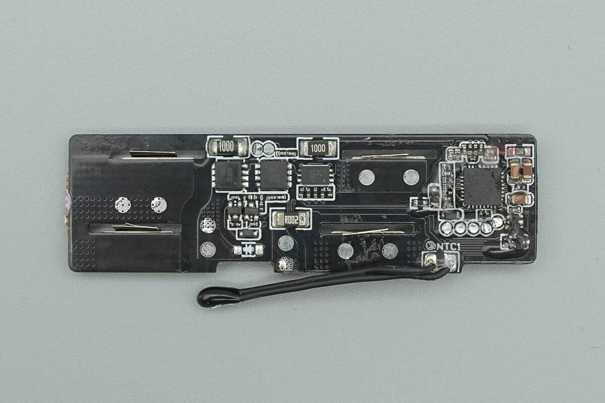
The back side contains components such as the battery protection chip and battery protection MOSFETs.
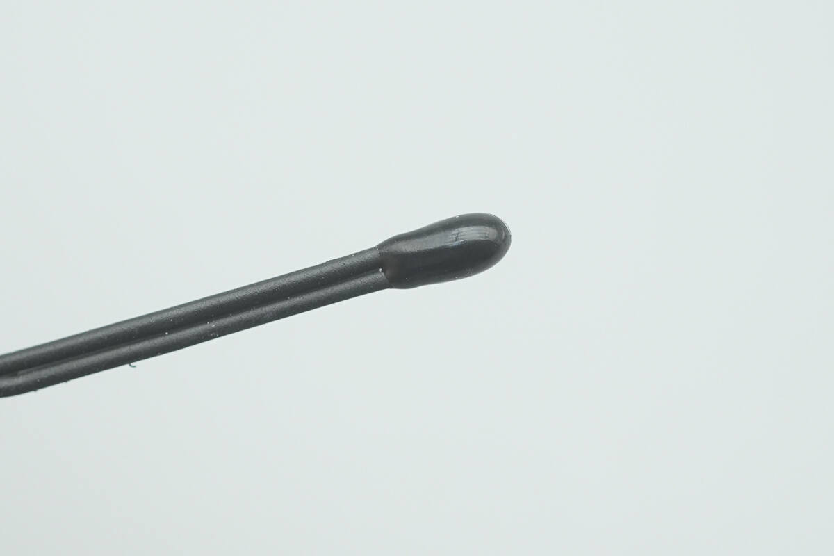
Close-up of the NTC thermistor.
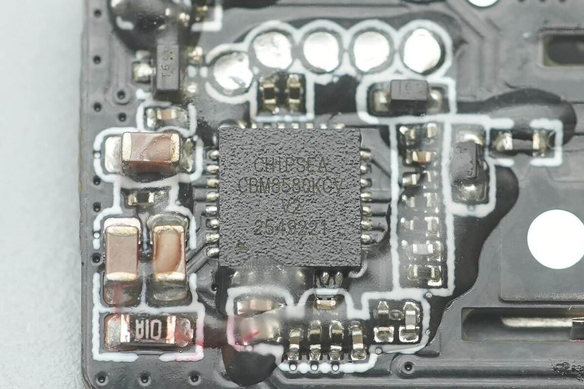
The battery protection chip is from Chipsea, model CBM8580KCV, part of the CBM8580 series. It is a single-chip, fully integrated BMS and high-precision fuel gauge designed for 2–4 series lithium batteries, packaged in a C-package.
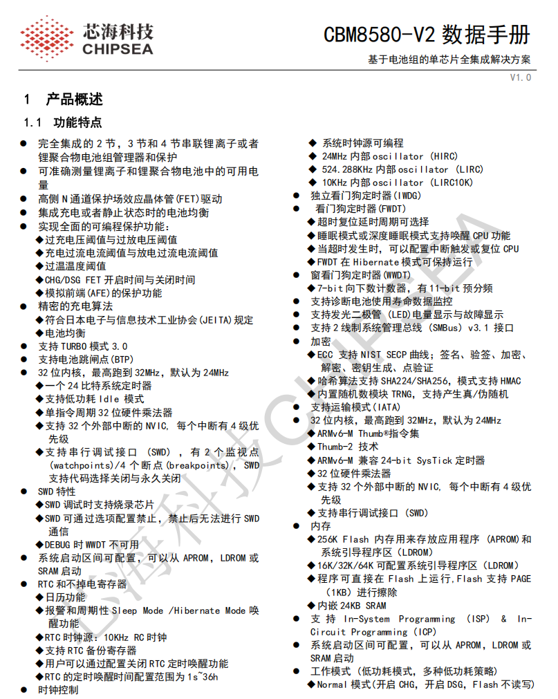
It provides capacity monitoring, protection, and certification functions for 2 to 4 series lithium battery packs. Using its integrated high-performance analog peripherals, it measures the available capacity, voltage, current, temperature, and other key parameters of the lithium batteries, maintains accurate data records, and reports this information to the system host controller via the communication interface.
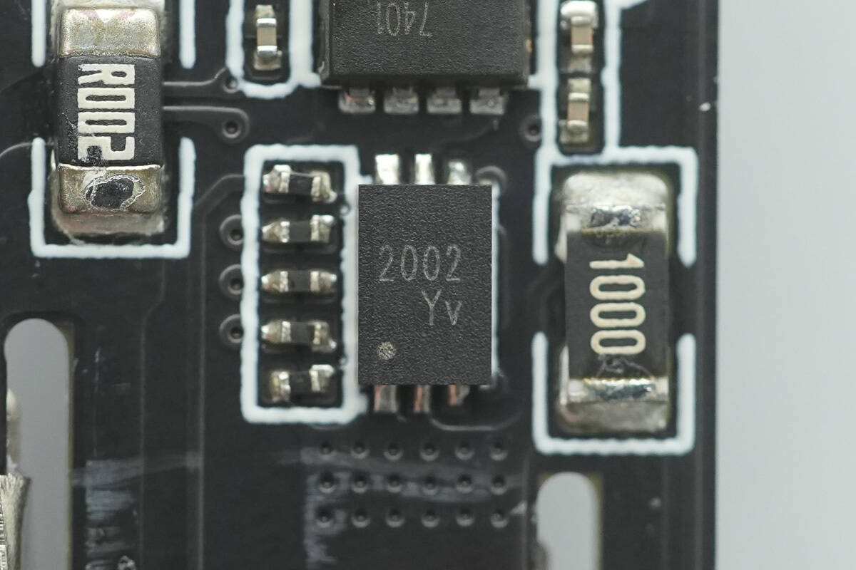
The battery protection MOSFETs, marked with 2002, are dual NMOS.
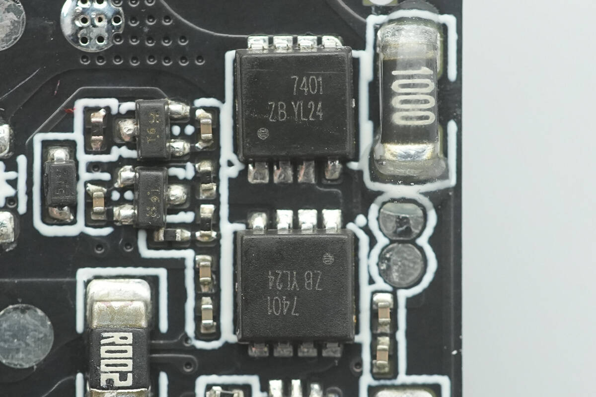
The other two battery protection MOSFETs are from Leadteck, model LT7401FLCB. They are PMOS with a voltage rating of –30 V and come in a PDFN3×3-8L package.
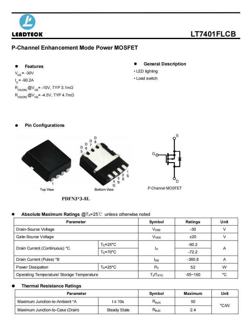
Here is the information about Leadteck LT7401FLCB.
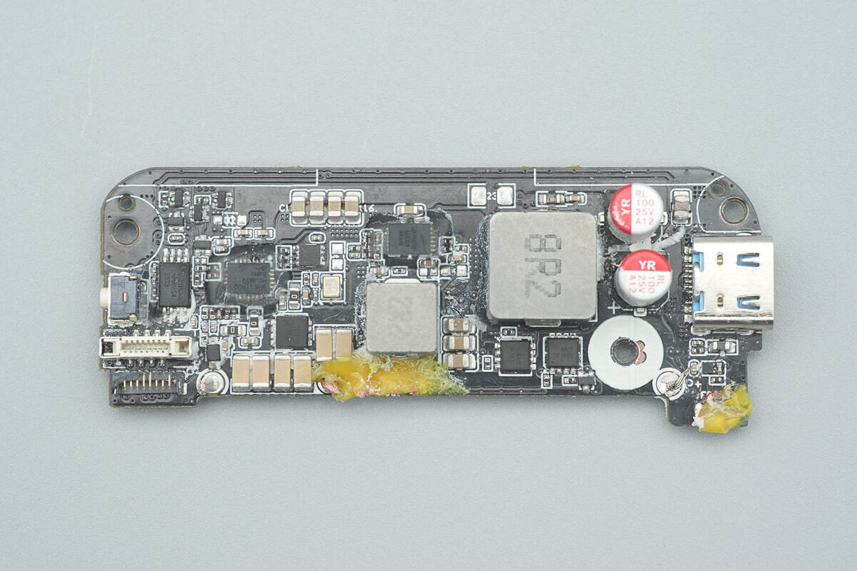
The front side of the PCBA contains components such as memory, the wireless charging master control chip, switching MOSFETs, synchronous boost converters, power control MOSFETs, and inductors.
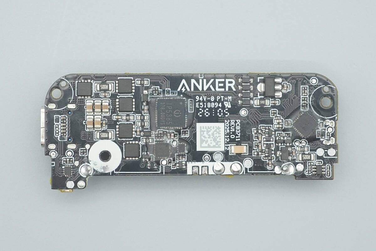
The back side contains the power bank master control chip, synchronous buck-boost MOSFETs, VBUS MOSFET, authentication chip, MCU, regulator chip, USB pass-through chip, current-sensing amplifier, and other components.
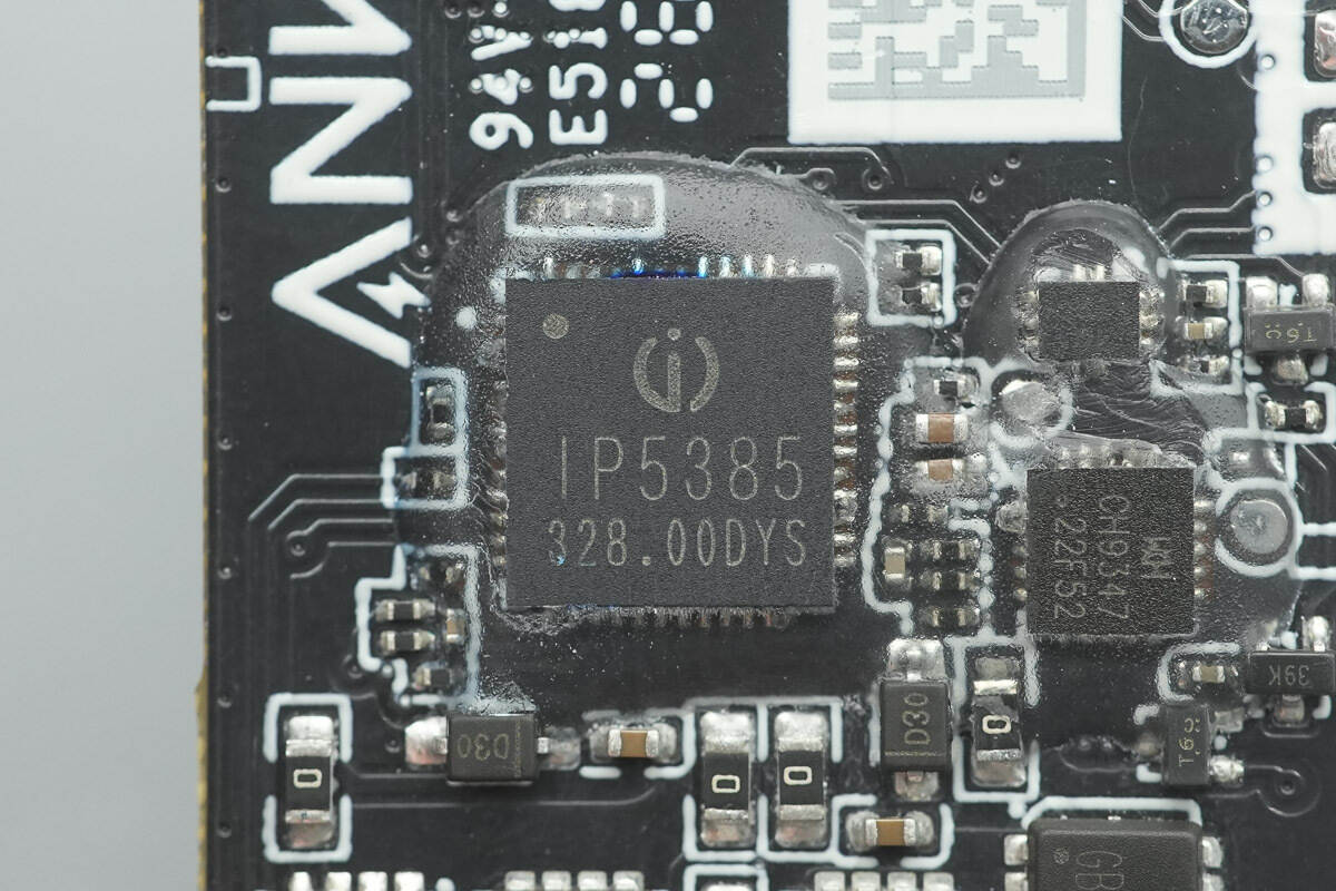
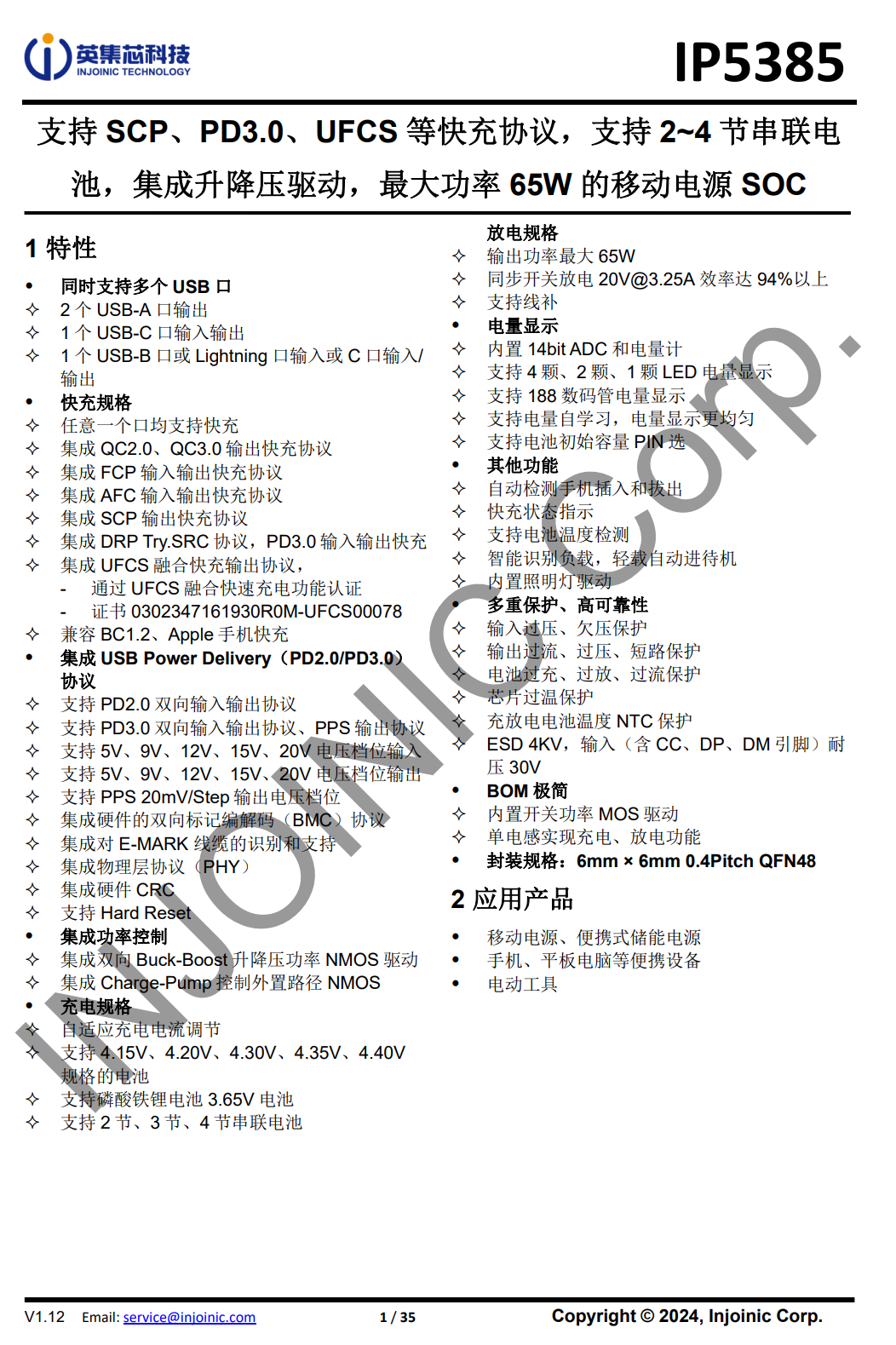
The power bank master control chip is from Injoinic, model IP5385. It is the industry's first integrated SOC for mobile power banks that combines UFCS with fast charging, featuring an integrated fast-charging protocol chip, MCU, and synchronous buck-boost controller. The chip supports 2–4 series lithium batteries as well as lithium iron phosphate batteries. By pairing with external MOSFETs and inductors, it can form a 65W bidirectional fast-charging mobile power bank.
It supports two USB-A output ports, one bidirectional USB-C port, and either a Lightning input or a USB-C input/output port. Any of these interfaces can deliver fast charging. The chip supports UFCS fast charging, PD3.0, and PPS, as well as Huawei SCP, FCP, and other fast-charging protocols.
The IP5385 features a built-in bidirectional synchronous buck-boost driver and an integrated charge pump, allowing the use of high-performance NMOS for switch control and path management. When paired with inductors, synchronous switches, and path management transistors corresponding to each interface, it can form a complete 2–4 series battery, multi-interface, high-power, fast-charging mobile power solution. It supports 65W charging and discharging power, suitable for mobile power banks, energy storage devices, portable equipment, and power tools.
Here is the information about Injoinic IP5385.
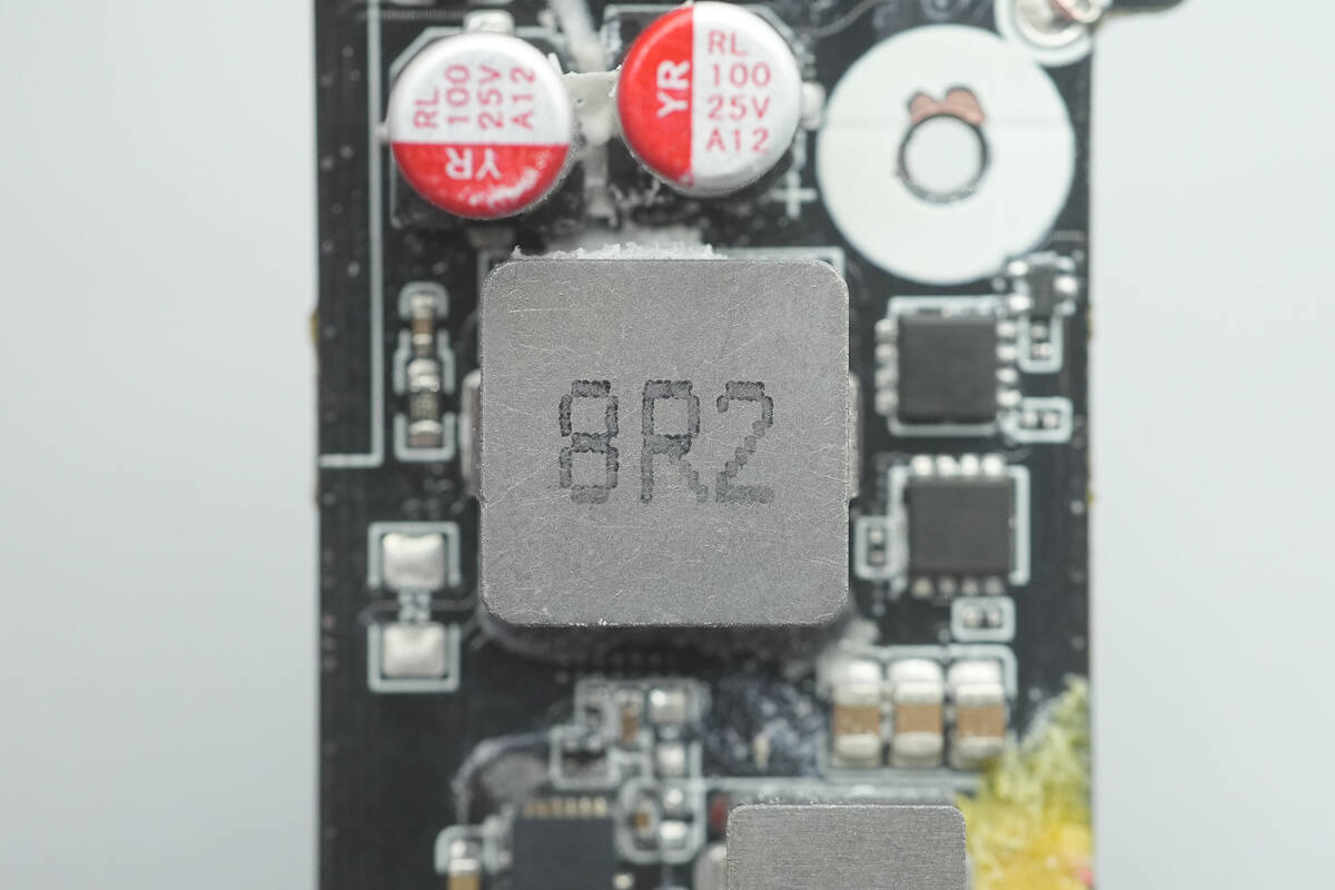
Close-up of the synchronous buck-boost alloy inductor.
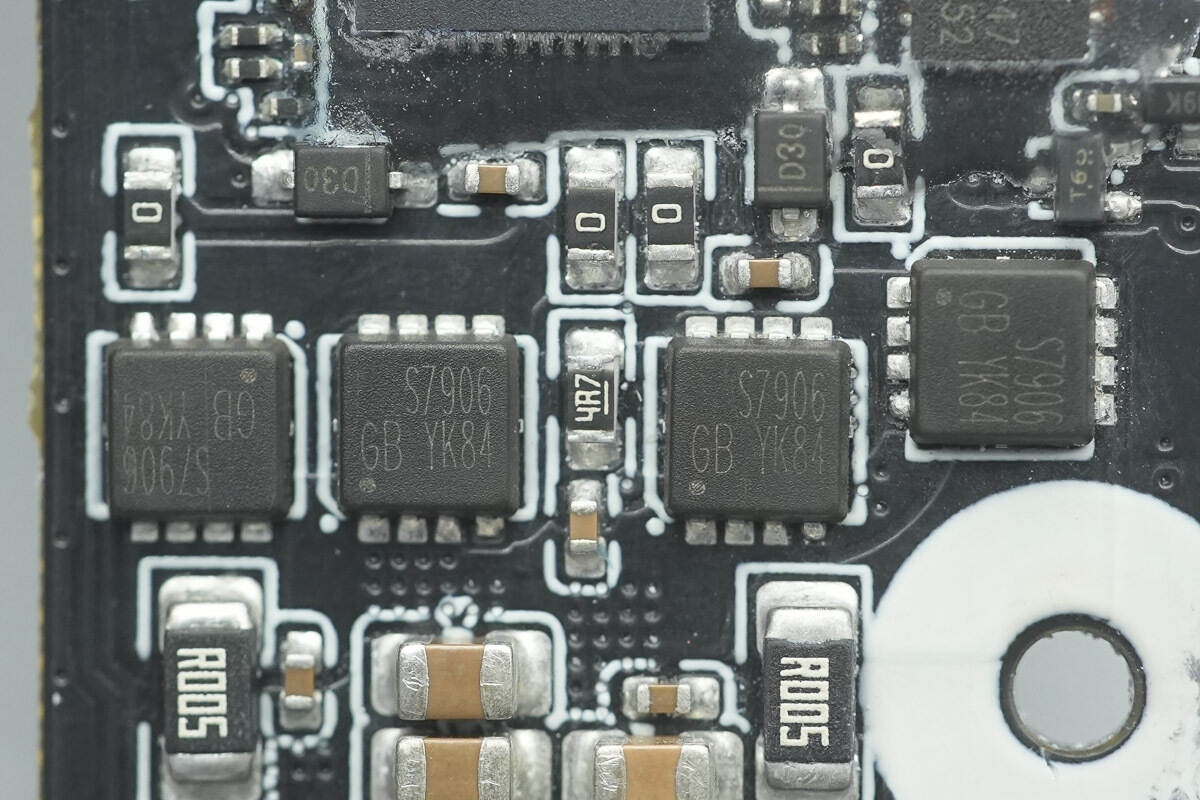
Four synchronous buck-boost MOSFETs marked S7906, from Leadteck, model LTS7906FL, NMOS, with a voltage rating of 30 V and an on-resistance of 3.1 mΩ, in a PDFN3×3-8L package.
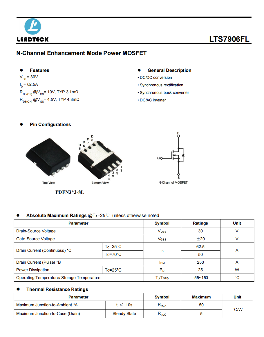
Here is the information about LTS7906FL.
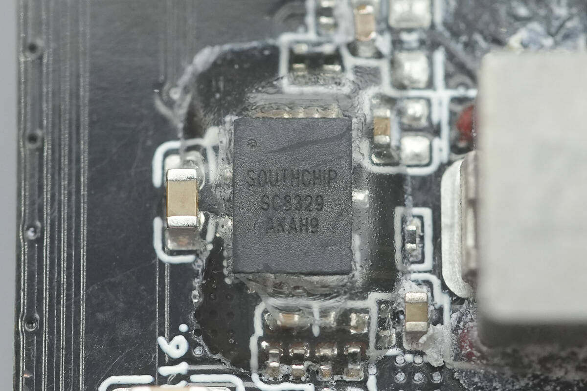
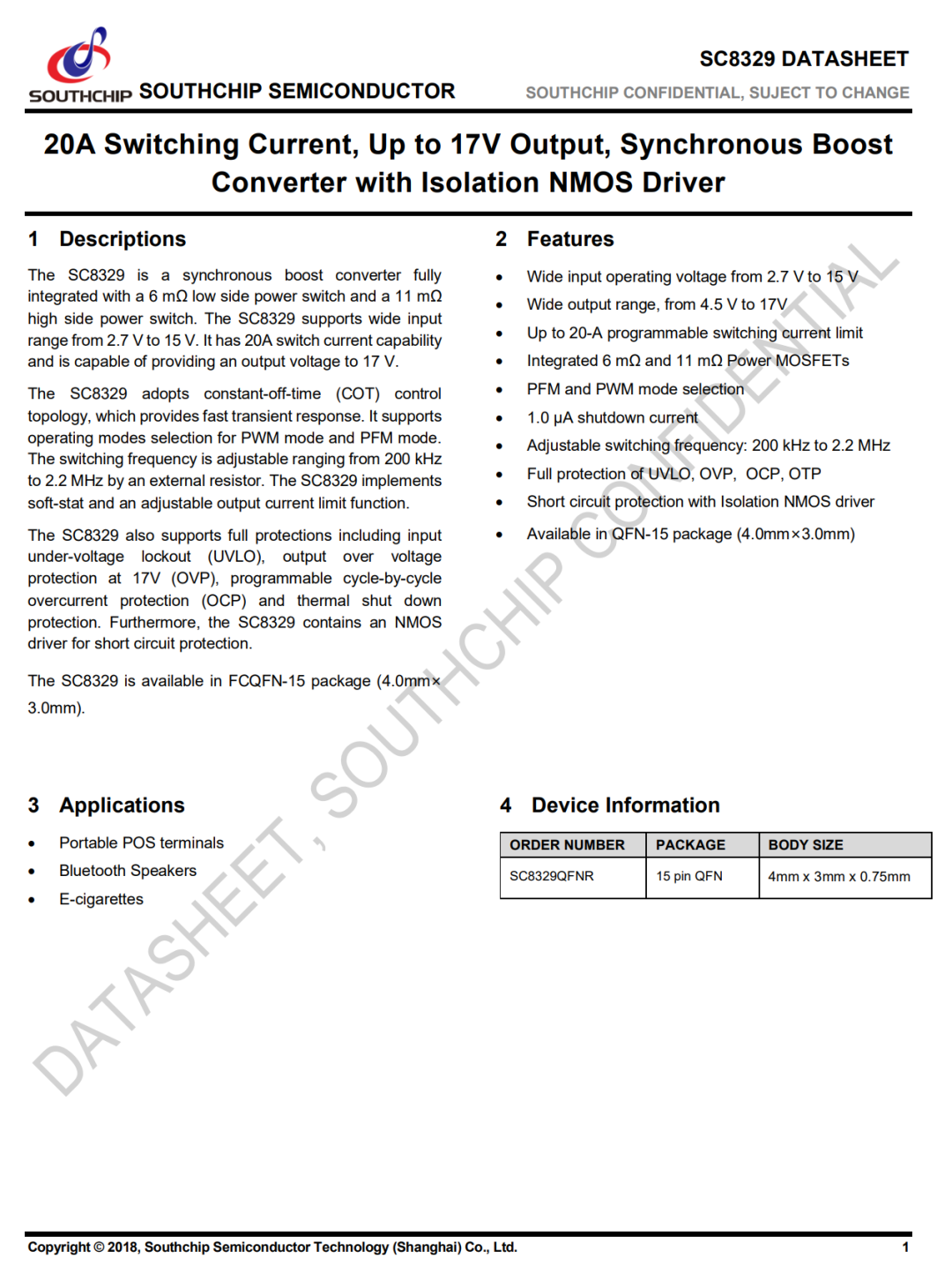
The synchronous boost converter is from SouthChip, model SC8329. It integrates a 6 mΩ MOSFET and an 11 mΩ synchronous rectifier. It supports an input voltage range of 2.7–13 V, with a maximum output voltage of 17 V. The device uses constant-off-time control and features fast transient response.
The SC8329 supports switching frequencies from 200 kHz to 2.2 MHz, adjustable via an external resistor. The chip also provides soft-start, adjustable output current limit, undervoltage lockout, output overvoltage protection, cycle-by-cycle overcurrent protection, and thermal shutdown protection.
Here is the information about SouthChip SC8329.
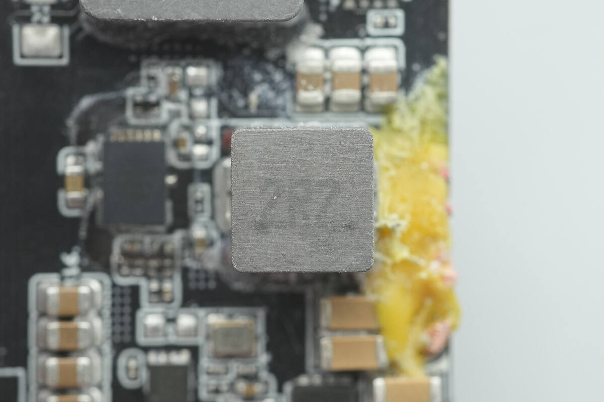
Close-up of the alloy boost inductor.
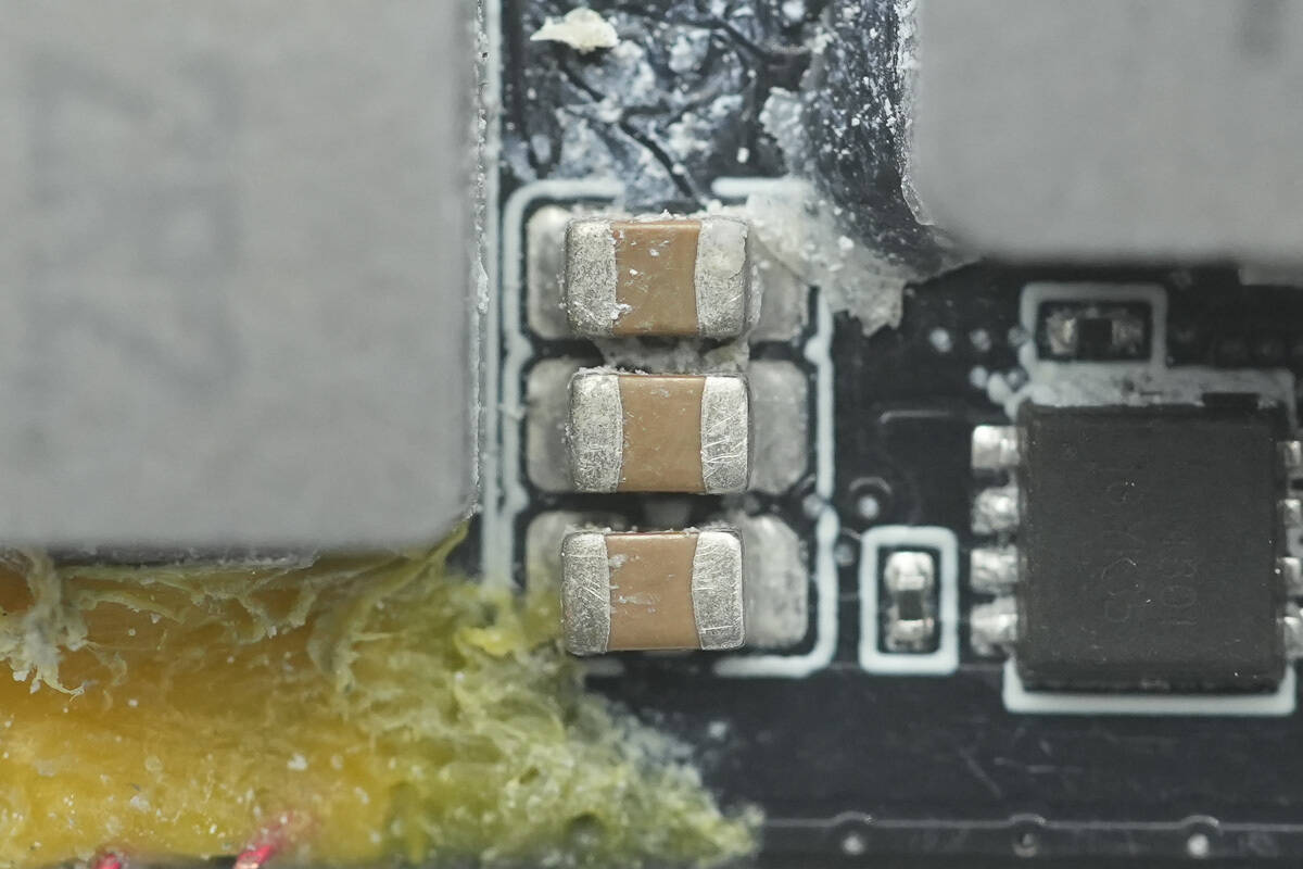
Three parallel MLCC capacitors are used for input filtering.
Close-up of the boost output filter capacitors.
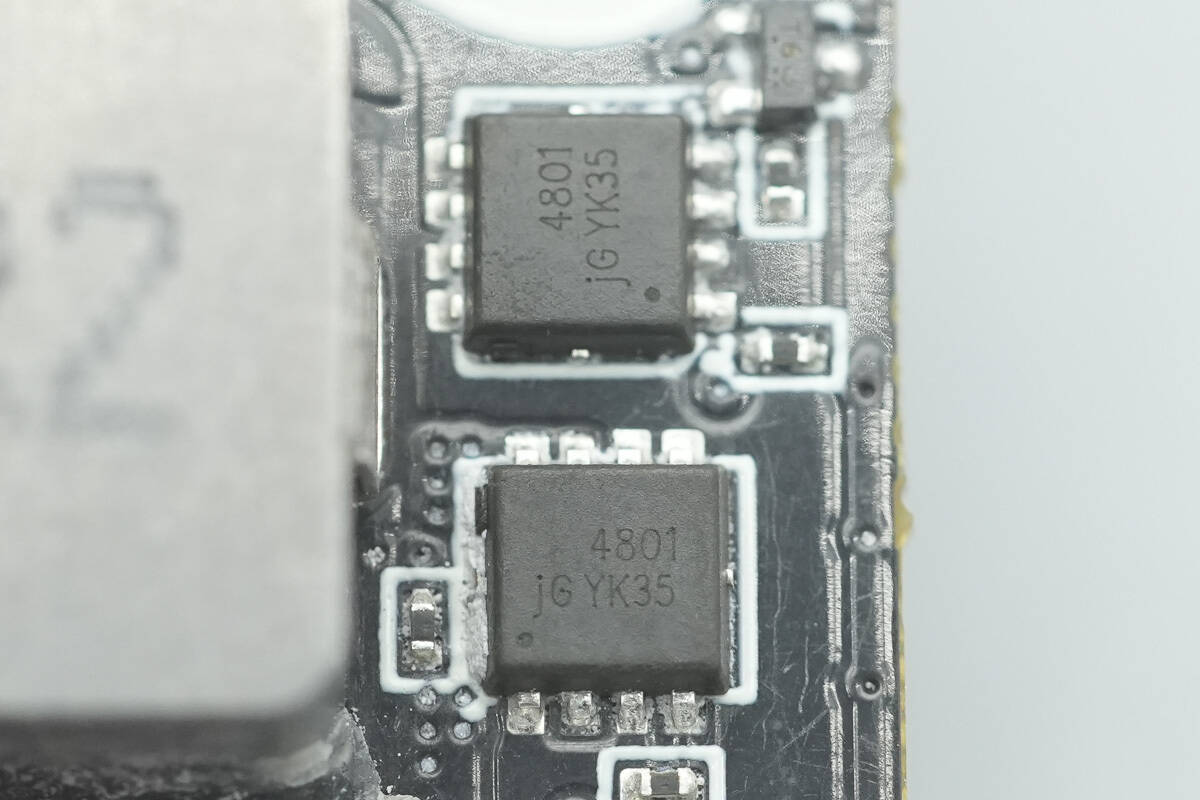
Two power control MOSFETs marked 4801.
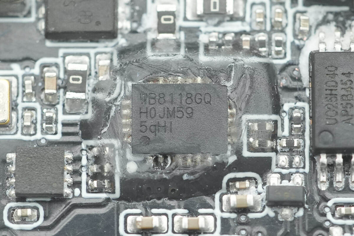
The wireless charging management chip is from CPS, model WB8118. WB8118 is a high-efficiency magnetic induction wireless power transmitter IC that supports Qi2 15W fast wireless charging. It features a wide input voltage range of 3.3 V to 18 V and is compatible with wireless power receiver (ASK) communication, with a fixed communication interface port. It provides reliable overvoltage, overcurrent, and temperature protection and comes in a QFN24 package.
The chip integrates a voltage regulator, full-bridge driver, ASK demodulator, FSK modulator, foreign object detection (FOD), PWM module, and a multi-channel 12-bit ADC.
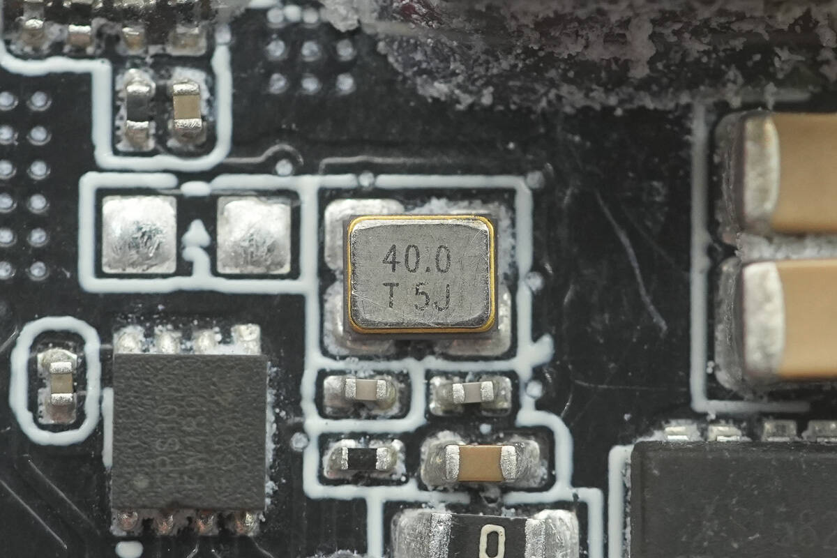
A 40.000 MHz passive crystal provides the clock for the wireless charging chip.
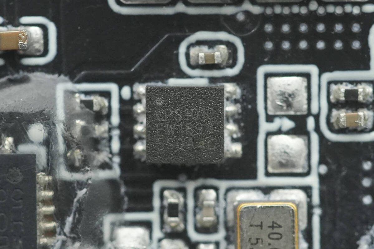
The authentication chip is from CPS, model CPS1010. It is a wireless charging protocol encryption chip designed for Qi-certified applications, integrating a SHA256 encryption engine, ECC signature, and true random number key generation. It provides identity authentication and security verification for wireless charging devices and comes in a DFN8 package.
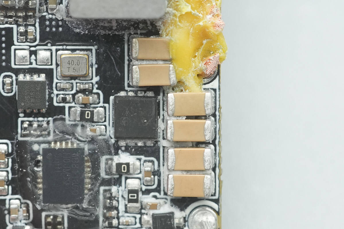
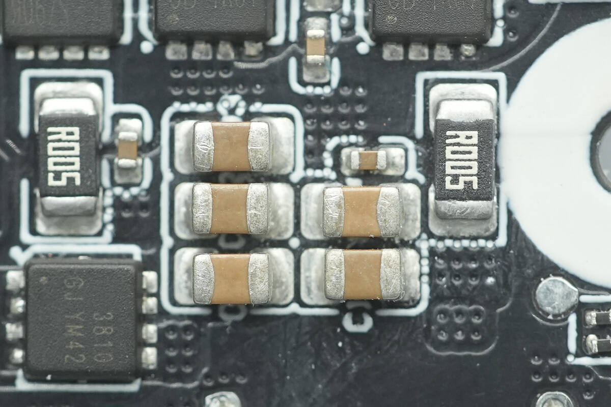
Close-up of the NPO resonant capacitors.
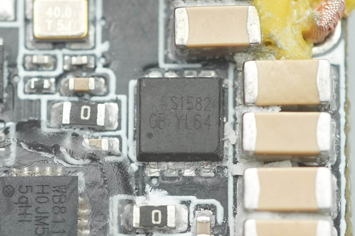
The switching MOSFET for the resonant capacitor is from Leadteck, model LTS1582FPC, a dual NMOS device with a voltage rating of 60 V and an on-resistance of 11 mΩ, in a PDFN3.3×3.3-8L package.
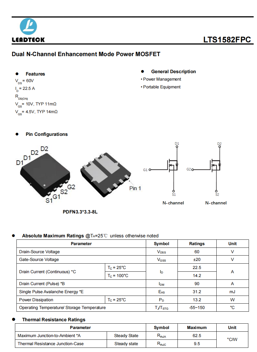
Here is the information about Leadteck LTS1582FPC.
Close-up of the toggle switch.
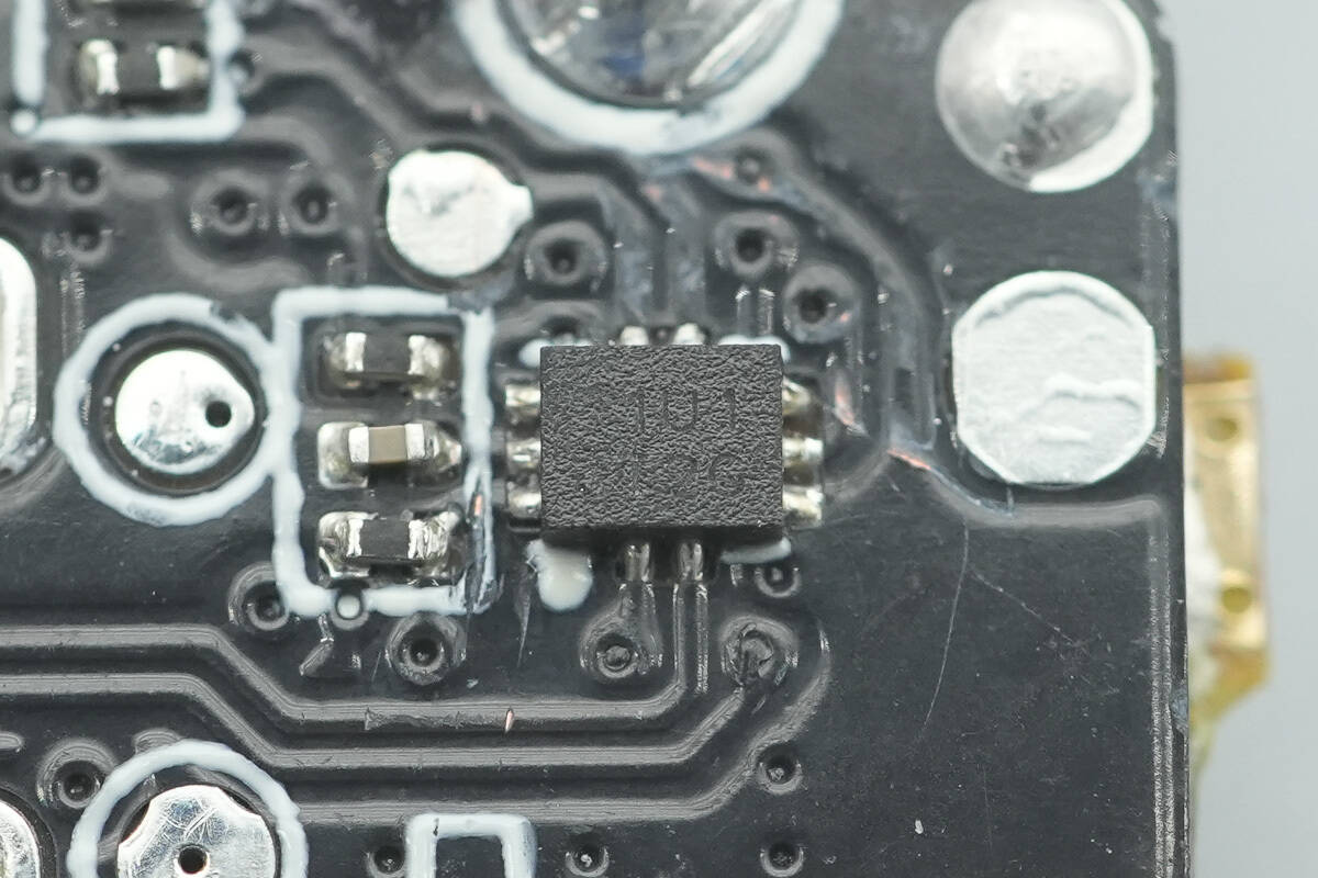
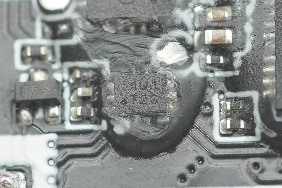
Two filtering solid capacitors are from RELON, rated 25 V, 100 μF.
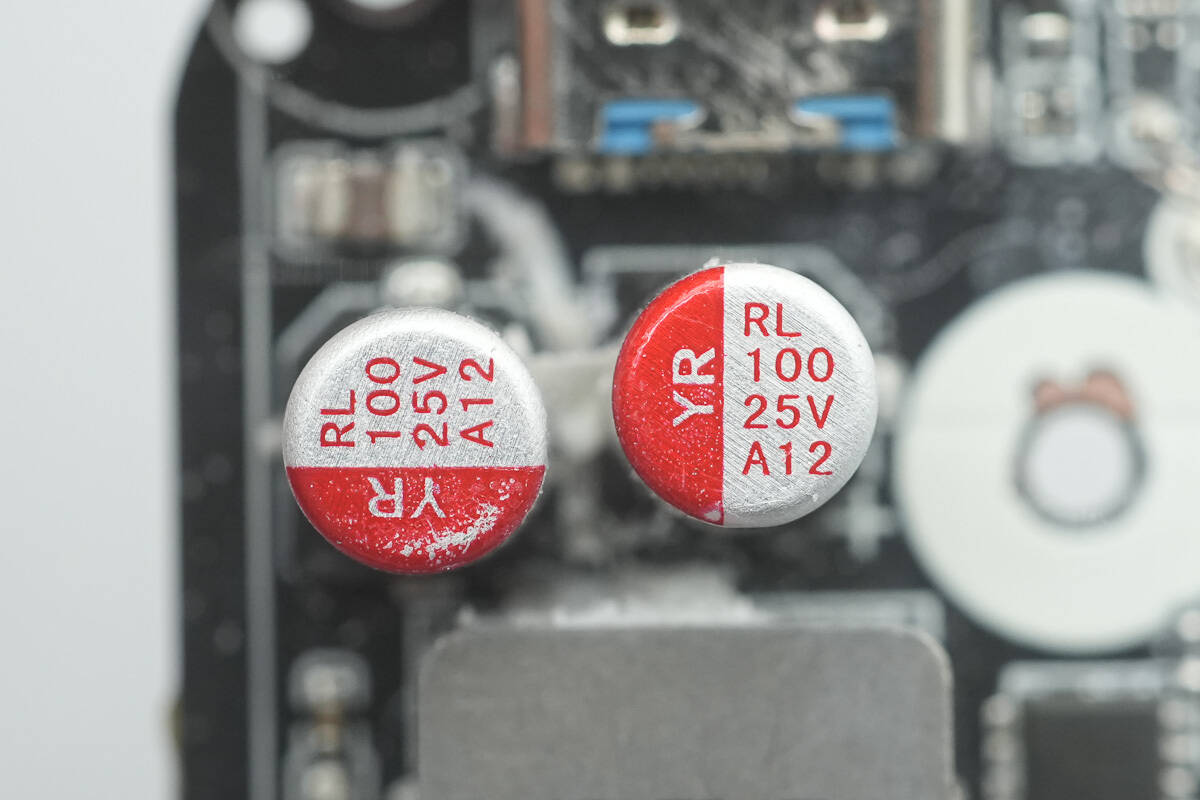
The VBUS MOSFET for the USB-C interface is from Leadteck, model LT3810FPJ, a dual NMOS device with a voltage rating of 30 V, in a DFN3×3-8L package.
Here is the information about Leadteck LT3810FPJ.
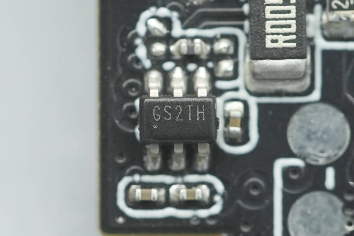
The current-sense amplifier marked GS2TH comes in a SOT23-6 package.
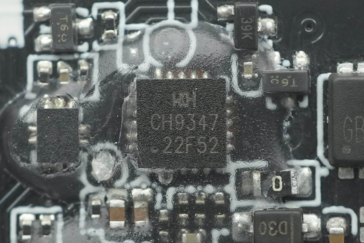
The USB passthrough chip is from WCH, model CH9347, in a QFN20 package. This chip enables the power bank to establish a communication link with smartphones and computer web interfaces, allowing key battery cell data measured by the controller to be transmitted directly via the USB interface to mobile phones and computers, thereby enabling battery data reading and interaction.
Close-up of the toggle switch.
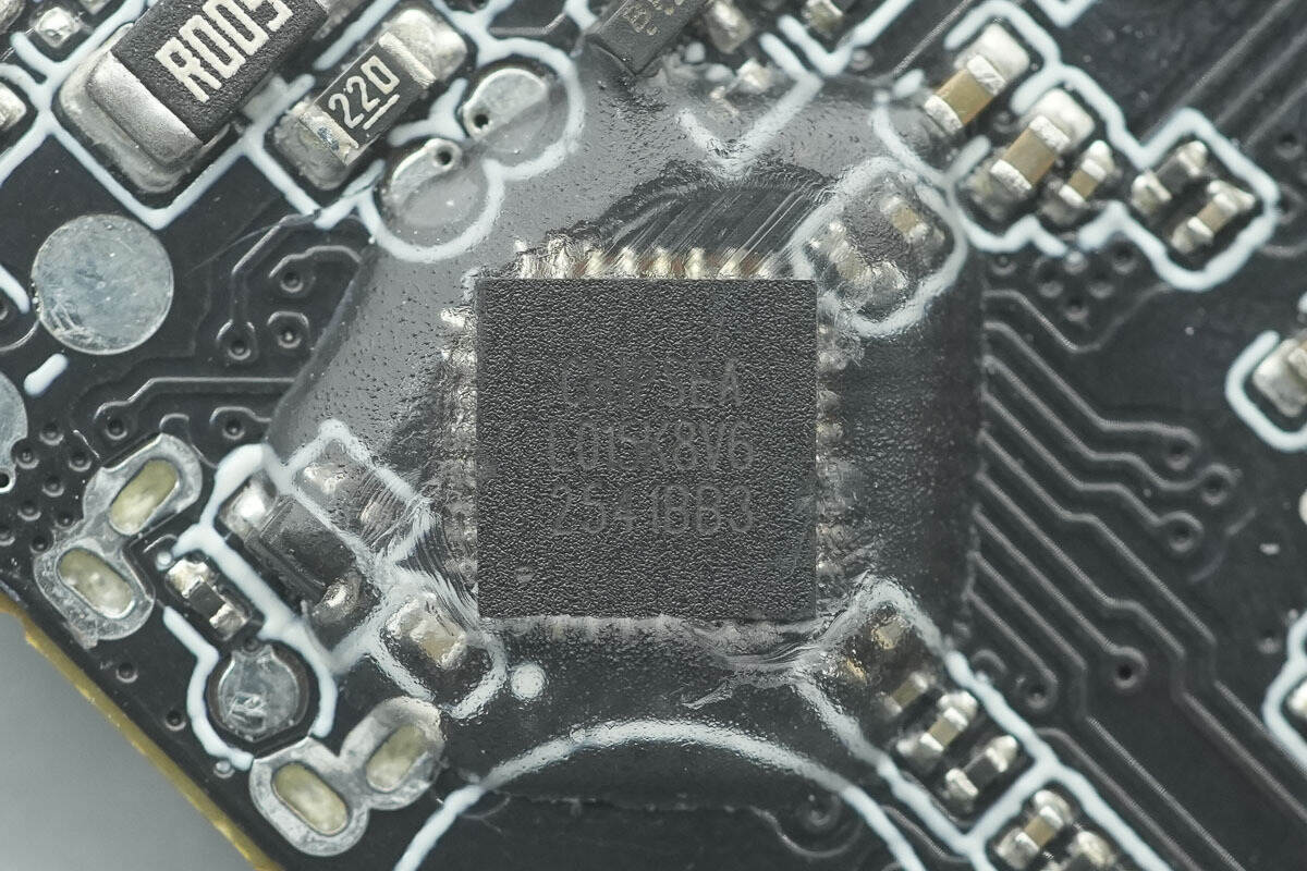
The MCU driving the digital display is from Chipsea, model CS32L015K8V6. It is an ultra-low-power microcontroller with a highly reliable 32-bit core, operating at a maximum frequency of 24 MHz. The chip features 64 KB embedded Flash, 8 KB SRAM, and integrates a 12-bit 1 Msps high-precision SAR ADC, RTC, comparator, operational amplifier, multiple UARTs, SPI, I²C, OWI, and PWM interfaces, offering high integration, strong anti-interference capability, and high reliability.
The chip operates over a temperature range of –40 °C to 85 °C and a voltage range of 2.5 V to 5.5 V. It comes in a QFN-32 (4×4 mm) package and provides multiple power modes to suit various low-power application scenarios. It is suitable for applications such as power banks, wearable devices, and personal care products.
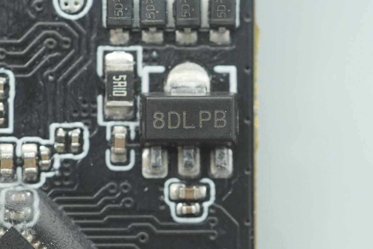
The regulator chip marked 8DLPB is used to supply power to the MCU.
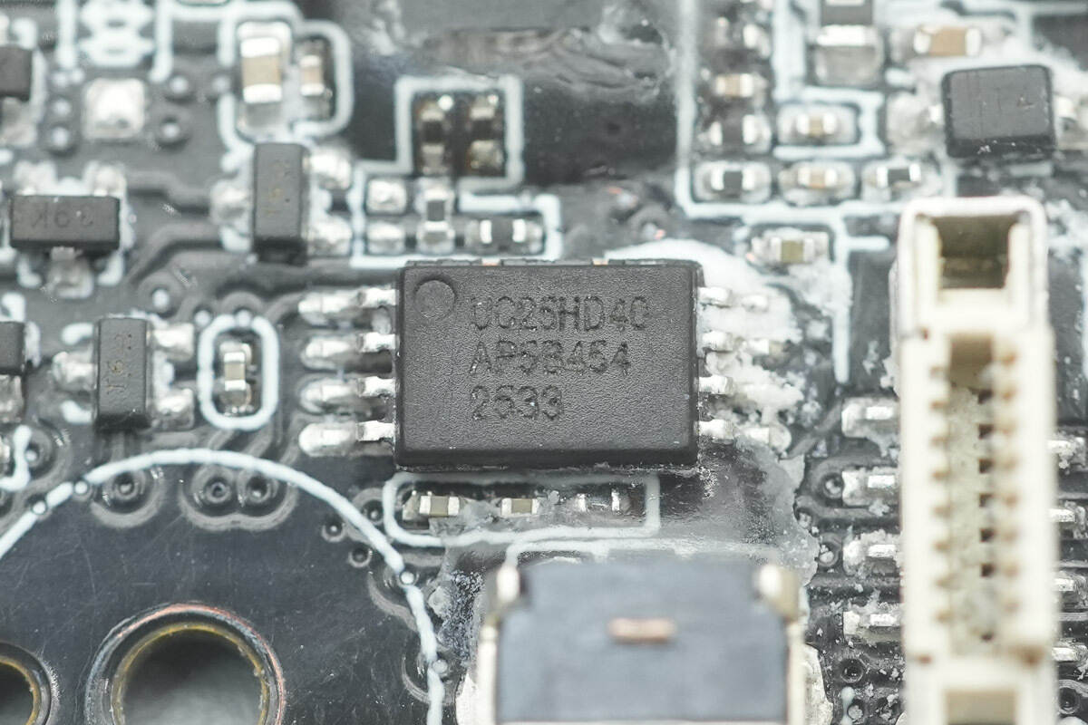
The memory is from UCUN, model UC25HD40. It is a 4 Mbit serial Flash memory, supporting SPI/DualSPI interfaces, and comes in a TSSOP8 package.
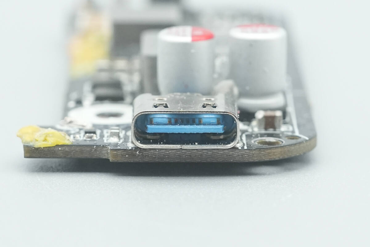
A close-up of the USB-C socket, featuring a blue plastic sheet.
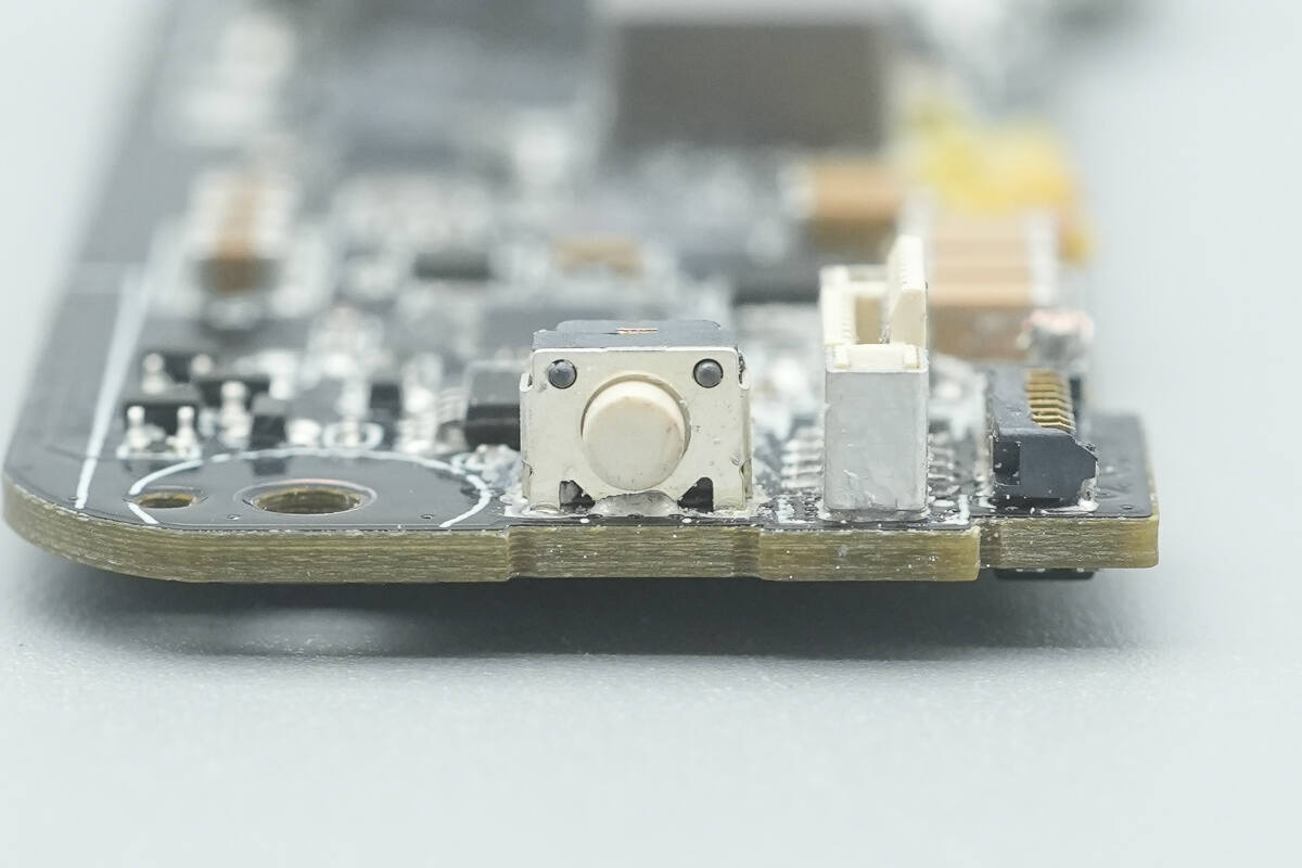
Close-up of the power button.
Well, those are all components of the Anker Nano 10000mAh Magnetic Wireless Charger Power Bank.
Summary of ChargerLAB
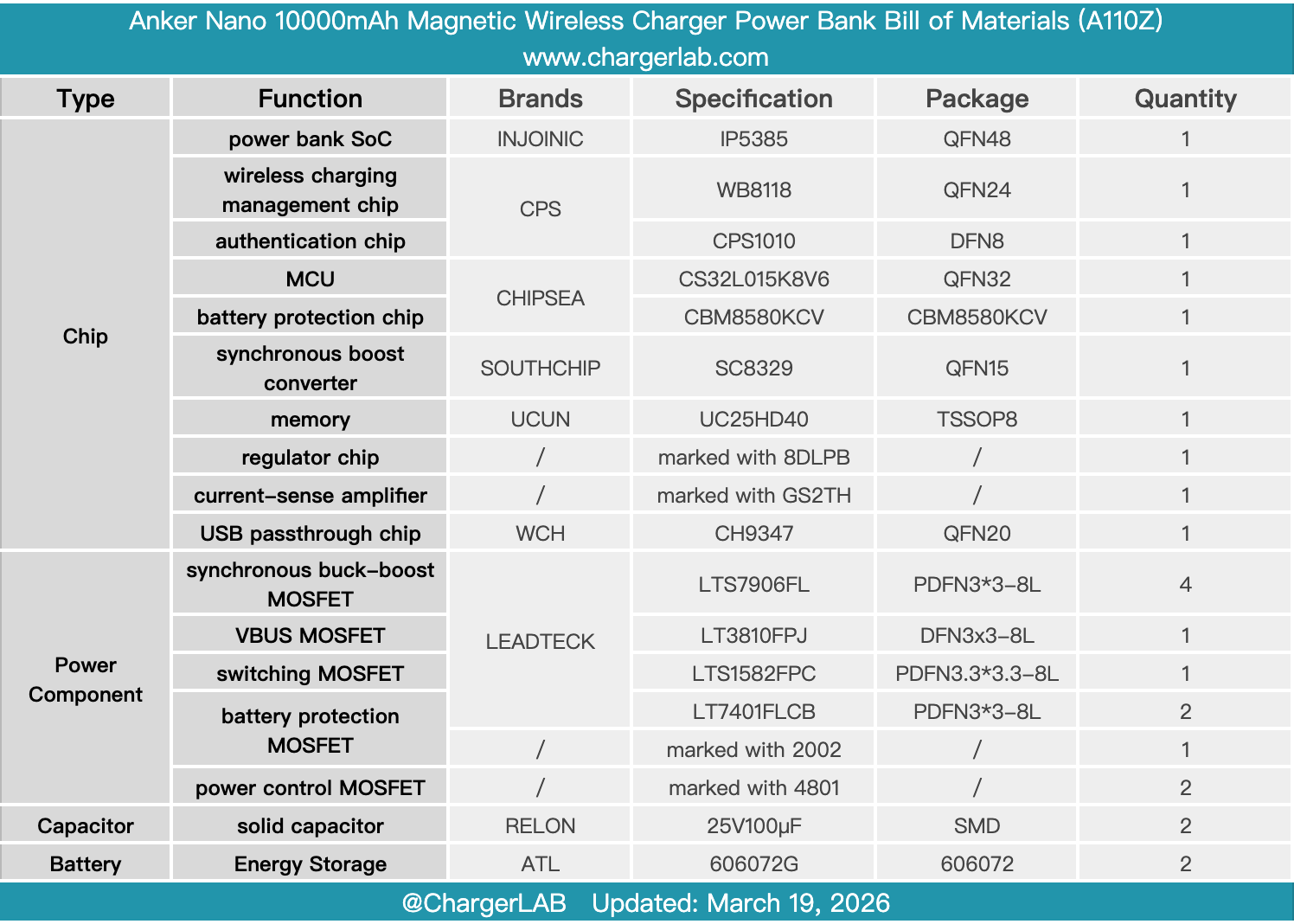
Here is the component list of the Anker Nano 10000mAh Magnetic Wireless Charger Power Bank for your convenience.
It supports 7.5 W wireless charging and 27 W wired output, as well as 20 W self-charging. A digital display shows the remaining battery level and estimated charging time. It features an integrated metal folding stand. The enclosure meets S.2 flame-retardant standards and has passed UL2056 secondary safety protection.
It also supports full transparent data tracking: when connected to a computer, the product model, serial number, battery health, cycle count, current, voltage, and individual cell status can all be viewed through a web interface.
After taking it apart, we found that the battery pack uses the Chipsea CBM8580KCV fully integrated chip for monitoring, protection, and data management. The power bank master control chip is the Injoinic IP5385, while the wireless charging section is implemented with a SouthChip SC8329 boost chip, a CPS WB8118 wireless charging management chip, and a CPS1010 authentication chip to form a complete solution. Data communication with the web interface is enabled via the WCH CH9347 USB passthrough chip, supplemented by the Chipsea CS32L015K8V6 MCU, which drives the digital display.
The battery pack consists of two ATL 5000 mAh pouch cells connected in series and is equipped with an NTC thermistor. The PCBA area is covered with a large area of thermal conductive gel, and graphene heat sinks, black foam, Qingke paper, high-temperature tape, and plastic insulating sheets are added at corresponding positions on the enclosure and battery cells. Key areas such as the coil, battery cells, PCBA, and hinge are provided with adequate insulation, cushioning, and auxiliary heat dissipation. The workmanship continues Anker’s consistent style of solid materials and build quality.
Related Articles:
1. Teardown of Apple 140W USB-C Power Adapter (A3607)
2. Teardown of HuntKey 65W Dual USB-C GaN Charger (H02)
3. Teardown of Samsung 60W Low Standby GaN Charger (EP-T6010)