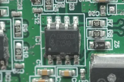
The race for smaller, more powerful chargers is hitting a new milestone. HYASiC has debuted the HYC935, a game-changing secondary-side controller that packs five essential components into one tiny QFN 5x5 package. By integrating the PD controller, SR controller, 100V NMOS, path MOSFET, and current-sensing resistor, HYASiC has effectively ended the era of cluttered, multi-chip secondary-side designs, allowing for significantly cleaner and more efficient power layouts.
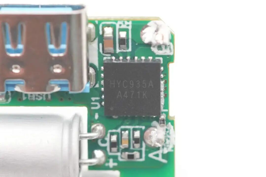
The HYC935 is a powerhouse of compatibility and protection. It supports the latest USB PD 3.1 and USB Type-C 2.2 standards, along with China’s UFCS protocol and a host of other mainstream standards like QC, SCP, and AFC. The chip excels in precision, offering dual-loop CV/CC control and programmable line-loss compensation to ensure stable voltage delivery even at high currents. Safety is built into its DNA, featuring a comprehensive protection suite (OVP, OCP, UVLO) and a dedicated NTC interface for real-time thermal monitoring. Plus, with support for online firmware updates, the chip is built to evolve with future protocol standards.
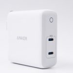
The HYC935 is already proving its worth in the real world—most notably in Anker’s popular Nano 30W GaN charger (A2147). By replacing five discrete components with this single, high-integration SoC, Anker successfully minimized PCB real estate, paving the way for the "thumb-sized" 30W charger that users love today. It is more than just a chip; it is the blueprint for the next generation of high-density, high-performance power products.
Related Articles:
1. Southchip SC8723: A High-Integration Solution for Compact Buck-Boost Power
2. iCM Chip Joins Tesla Supply Chain: A Milestone for China’s Semiconductor Industry
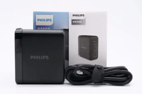
3. RUNXIN's GaN Chips Enter Philips Supply Chain